EP1042529B1 - Method for selectively depositing bismuth based ferroelectric films - Google Patents
Method for selectively depositing bismuth based ferroelectric films Download PDFInfo
- Publication number
- EP1042529B1 EP1042529B1 EP98963936A EP98963936A EP1042529B1 EP 1042529 B1 EP1042529 B1 EP 1042529B1 EP 98963936 A EP98963936 A EP 98963936A EP 98963936 A EP98963936 A EP 98963936A EP 1042529 B1 EP1042529 B1 EP 1042529B1
- Authority
- EP
- European Patent Office
- Prior art keywords
- accordance
- bismuth
- deposited
- substrate
- range
- Prior art date
- Legal status (The legal status is an assumption and is not a legal conclusion. Google has not performed a legal analysis and makes no representation as to the accuracy of the status listed.)
- Expired - Lifetime
Links
Images



Classifications
-
- H—ELECTRICITY
- H10—SEMICONDUCTOR DEVICES; ELECTRIC SOLID-STATE DEVICES NOT OTHERWISE PROVIDED FOR
- H10P—GENERIC PROCESSES OR APPARATUS FOR THE MANUFACTURE OR TREATMENT OF DEVICES COVERED BY CLASS H10
- H10P14/00—Formation of materials, e.g. in the shape of layers or pillars
- H10P14/60—Formation of materials, e.g. in the shape of layers or pillars of insulating materials
- H10P14/63—Formation of materials, e.g. in the shape of layers or pillars of insulating materials characterised by the formation processes
- H10P14/6326—Deposition processes
- H10P14/6328—Deposition from the gas or vapour phase
- H10P14/6334—Deposition from the gas or vapour phase using decomposition or reaction of gaseous or vapour phase compounds, i.e. chemical vapour deposition
-
- C—CHEMISTRY; METALLURGY
- C07—ORGANIC CHEMISTRY
- C07F—ACYCLIC, CARBOCYCLIC OR HETEROCYCLIC COMPOUNDS CONTAINING ELEMENTS OTHER THAN CARBON, HYDROGEN, HALOGEN, OXYGEN, NITROGEN, SULFUR, SELENIUM OR TELLURIUM
- C07F9/00—Compounds containing elements of Groups 5 or 15 of the Periodic Table
- C07F9/94—Bismuth compounds
-
- C—CHEMISTRY; METALLURGY
- C23—COATING METALLIC MATERIAL; COATING MATERIAL WITH METALLIC MATERIAL; CHEMICAL SURFACE TREATMENT; DIFFUSION TREATMENT OF METALLIC MATERIAL; COATING BY VACUUM EVAPORATION, BY SPUTTERING, BY ION IMPLANTATION OR BY CHEMICAL VAPOUR DEPOSITION, IN GENERAL; INHIBITING CORROSION OF METALLIC MATERIAL OR INCRUSTATION IN GENERAL
- C23C—COATING METALLIC MATERIAL; COATING MATERIAL WITH METALLIC MATERIAL; SURFACE TREATMENT OF METALLIC MATERIAL BY DIFFUSION INTO THE SURFACE, BY CHEMICAL CONVERSION OR SUBSTITUTION; COATING BY VACUUM EVAPORATION, BY SPUTTERING, BY ION IMPLANTATION OR BY CHEMICAL VAPOUR DEPOSITION, IN GENERAL
- C23C16/00—Chemical coating by decomposition of gaseous compounds, without leaving reaction products of surface material in the coating, i.e. chemical vapour deposition [CVD] processes
- C23C16/04—Coating on selected surface areas, e.g. using masks
-
- C—CHEMISTRY; METALLURGY
- C23—COATING METALLIC MATERIAL; COATING MATERIAL WITH METALLIC MATERIAL; CHEMICAL SURFACE TREATMENT; DIFFUSION TREATMENT OF METALLIC MATERIAL; COATING BY VACUUM EVAPORATION, BY SPUTTERING, BY ION IMPLANTATION OR BY CHEMICAL VAPOUR DEPOSITION, IN GENERAL; INHIBITING CORROSION OF METALLIC MATERIAL OR INCRUSTATION IN GENERAL
- C23C—COATING METALLIC MATERIAL; COATING MATERIAL WITH METALLIC MATERIAL; SURFACE TREATMENT OF METALLIC MATERIAL BY DIFFUSION INTO THE SURFACE, BY CHEMICAL CONVERSION OR SUBSTITUTION; COATING BY VACUUM EVAPORATION, BY SPUTTERING, BY ION IMPLANTATION OR BY CHEMICAL VAPOUR DEPOSITION, IN GENERAL
- C23C16/00—Chemical coating by decomposition of gaseous compounds, without leaving reaction products of surface material in the coating, i.e. chemical vapour deposition [CVD] processes
- C23C16/22—Chemical coating by decomposition of gaseous compounds, without leaving reaction products of surface material in the coating, i.e. chemical vapour deposition [CVD] processes characterised by the deposition of inorganic material, other than metallic material
- C23C16/30—Deposition of compounds, mixtures or solid solutions, e.g. borides, carbides, nitrides
- C23C16/40—Oxides
-
- C—CHEMISTRY; METALLURGY
- C23—COATING METALLIC MATERIAL; COATING MATERIAL WITH METALLIC MATERIAL; CHEMICAL SURFACE TREATMENT; DIFFUSION TREATMENT OF METALLIC MATERIAL; COATING BY VACUUM EVAPORATION, BY SPUTTERING, BY ION IMPLANTATION OR BY CHEMICAL VAPOUR DEPOSITION, IN GENERAL; INHIBITING CORROSION OF METALLIC MATERIAL OR INCRUSTATION IN GENERAL
- C23C—COATING METALLIC MATERIAL; COATING MATERIAL WITH METALLIC MATERIAL; SURFACE TREATMENT OF METALLIC MATERIAL BY DIFFUSION INTO THE SURFACE, BY CHEMICAL CONVERSION OR SUBSTITUTION; COATING BY VACUUM EVAPORATION, BY SPUTTERING, BY ION IMPLANTATION OR BY CHEMICAL VAPOUR DEPOSITION, IN GENERAL
- C23C16/00—Chemical coating by decomposition of gaseous compounds, without leaving reaction products of surface material in the coating, i.e. chemical vapour deposition [CVD] processes
- C23C16/44—Chemical coating by decomposition of gaseous compounds, without leaving reaction products of surface material in the coating, i.e. chemical vapour deposition [CVD] processes characterised by the method of coating
- C23C16/455—Chemical coating by decomposition of gaseous compounds, without leaving reaction products of surface material in the coating, i.e. chemical vapour deposition [CVD] processes characterised by the method of coating characterised by the method used for introducing gases into reaction chamber or for modifying gas flows in reaction chamber
- C23C16/45512—Premixing before introduction in the reaction chamber
-
- H—ELECTRICITY
- H10—SEMICONDUCTOR DEVICES; ELECTRIC SOLID-STATE DEVICES NOT OTHERWISE PROVIDED FOR
- H10D—INORGANIC ELECTRIC SEMICONDUCTOR DEVICES
- H10D1/00—Resistors, capacitors or inductors
- H10D1/60—Capacitors
- H10D1/68—Capacitors having no potential barriers
- H10D1/682—Capacitors having no potential barriers having dielectrics comprising perovskite structures
-
- H—ELECTRICITY
- H10—SEMICONDUCTOR DEVICES; ELECTRIC SOLID-STATE DEVICES NOT OTHERWISE PROVIDED FOR
- H10P—GENERIC PROCESSES OR APPARATUS FOR THE MANUFACTURE OR TREATMENT OF DEVICES COVERED BY CLASS H10
- H10P14/00—Formation of materials, e.g. in the shape of layers or pillars
- H10P14/60—Formation of materials, e.g. in the shape of layers or pillars of insulating materials
- H10P14/66—Formation of materials, e.g. in the shape of layers or pillars of insulating materials characterised by the type of materials
- H10P14/668—Formation of materials, e.g. in the shape of layers or pillars of insulating materials characterised by the type of materials the materials being characterised by the deposition precursor materials
-
- H—ELECTRICITY
- H10—SEMICONDUCTOR DEVICES; ELECTRIC SOLID-STATE DEVICES NOT OTHERWISE PROVIDED FOR
- H10P—GENERIC PROCESSES OR APPARATUS FOR THE MANUFACTURE OR TREATMENT OF DEVICES COVERED BY CLASS H10
- H10P14/00—Formation of materials, e.g. in the shape of layers or pillars
- H10P14/60—Formation of materials, e.g. in the shape of layers or pillars of insulating materials
- H10P14/69—Inorganic materials
- H10P14/692—Inorganic materials composed of oxides, glassy oxides or oxide-based glasses
- H10P14/6921—Inorganic materials composed of oxides, glassy oxides or oxide-based glasses containing silicon
- H10P14/69215—Inorganic materials composed of oxides, glassy oxides or oxide-based glasses containing silicon the material being a silicon oxide, e.g. SiO2
-
- H—ELECTRICITY
- H10—SEMICONDUCTOR DEVICES; ELECTRIC SOLID-STATE DEVICES NOT OTHERWISE PROVIDED FOR
- H10P—GENERIC PROCESSES OR APPARATUS FOR THE MANUFACTURE OR TREATMENT OF DEVICES COVERED BY CLASS H10
- H10P14/00—Formation of materials, e.g. in the shape of layers or pillars
- H10P14/60—Formation of materials, e.g. in the shape of layers or pillars of insulating materials
- H10P14/69—Inorganic materials
- H10P14/692—Inorganic materials composed of oxides, glassy oxides or oxide-based glasses
- H10P14/6938—Inorganic materials composed of oxides, glassy oxides or oxide-based glasses the material containing at least one metal element, e.g. metal oxides, metal oxynitrides or metal oxycarbides
- H10P14/69398—Inorganic materials composed of oxides, glassy oxides or oxide-based glasses the material containing at least one metal element, e.g. metal oxides, metal oxynitrides or metal oxycarbides the material having a perovskite structure, e.g. BaTiO3
-
- H—ELECTRICITY
- H10—SEMICONDUCTOR DEVICES; ELECTRIC SOLID-STATE DEVICES NOT OTHERWISE PROVIDED FOR
- H10P—GENERIC PROCESSES OR APPARATUS FOR THE MANUFACTURE OR TREATMENT OF DEVICES COVERED BY CLASS H10
- H10P14/00—Formation of materials, e.g. in the shape of layers or pillars
- H10P14/60—Formation of materials, e.g. in the shape of layers or pillars of insulating materials
- H10P14/69—Inorganic materials
- H10P14/694—Inorganic materials composed of nitrides
- H10P14/6943—Inorganic materials composed of nitrides containing silicon
- H10P14/69433—Inorganic materials composed of nitrides containing silicon the material being a silicon nitride not containing oxygen, e.g. SixNy or SixByNz
Definitions
- This invention relates to a method for the selective deposition of bismuth based ceramic thin films. More specifically, the present invention relates to the preparation of bismuth based ferroelectric thin films by selective chemical vapor deposition.
- ferroelectric materials which have found wide use in random access memory applications.
- ferroelectric capacitors which typically evidence high remanent polarization, small size, low leakage current and low fatigue rate. Accordingly, workers in the art have focused their interest upon the development of suitable techniques for the growth of ferroelectric thin films with optimum characteristics.
- SBT SrBi 2 Ta 2 O 9
- Desu et al. in U.S. Patent No. 5,527,567 disclosed a method for the deposition by chemical vapor deposition techniques of high quality layered structured oxide ferroelectric thin films. These films were deposited at temperatures ranging from 450-800°C. The patentees specifically noted that at temperatures greater than 650°C poor quality films were produced whereas at temperatures less than 600°C excellent quality films were obtained.
- Selectivity in the deposition process is attained by selection of substrate/insulating material combinations which assure high Bi 2 O 3 deposition efficiency on the electrically conductive material and low Bi 2 O 3 deposition efficiency on the insulating material in combination with controlled process parameters.
- selectivity in the deposition process may be effected by the use of an oxide phase during the time frame in which Bi 2 O 3 deposition efficiency is high or by means of a thin auxiliary layer deposited upon the electrode.
- FIG. 1a there is shown a front elevational view in cross-section of a typical ferroelectric random access memory cell (FRAM). Shown in the figure is an insulating substrate 11, typically silicon dioxide (SiO 2 ) or silicon nitride (Si 3 N 4 ), on top of a silicon substrate. At the interface between both substrates but embedded into the silicon substrate is a CMOS transistor including source 12, drain 13 and gate 14. Source 12 and gate 14 are connected to bit line 15 and word line 16, respectively. Drain 13 is connected to plug 14 which is designed to serve as connection to a stack capacitor having a bottom electrode, a ferroelectric layer and an upper electrode layer.
- FRAM ferroelectric random access memory cell
- Fig. 1b shows the structure of Fig. 1a after the deposition thereon of the optional barrier layer 17. Absent this barrier layer, there is a possibility that oxidation will occur, so resulting in the interruption of the electrical connection between the bottom electrode and the drain. Additionally, the barrier layer tends to preclude diffusion of atoms from the electrode or the ferroelectric material into the plug. Also shown in Fig.
- bottom electrode 18 of the capacitor typically comprising a noble metal selected from among platinum, palladium, rhodium, gold and ruthenium, a conductive metal oxide selected from among ruthenium oxide, osmium oxide, rhenium oxide, rhodium oxide, iridium oxide, or mixed metal oxides such as LSCO, YBCO and metal nitrides such as titanium nitride or zirconium nitride.
- a noble metal selected from among platinum, palladium, rhodium, gold and ruthenium
- a conductive metal oxide selected from among ruthenium oxide, osmium oxide, rhenium oxide, rhodium oxide, iridium oxide, or mixed metal oxides such as LSCO, YBCO and metal nitrides such as titanium nitride or zirconium nitride.
- the invention relates to the selective deposition of Bi-containing ferroelectric films.
- Bi-containing are formed by, for example, using a diketonate Bi precursor as is known in the art.
- the next step in the fabrication of the desired FRAM involves structuring the barrier layer and bottom electrode by conventional photolithographic techniques.
- the resultant structure is shown in Fig. 1c.
- the novel process for the selective deposition of SBT is effected.
- the presence of two substrates, that is, the bottom electrode 18 and the base member 11 in combination with specific processing parameters is the focus of the present invention. It is an object of the invention to assure that deposition of the SBT occurs preferentially on the bottom electrode and either does not deposit on the substrate base or does so to a limited extent. This end is enhanced by initially providing the bottom electrode with a high density of absorption sites and choosing an electrode material which is catalytically active. Each of these characteristics will assure high deposition rates for bismuth oxide.
- Noble metals and alloys containing noble metals or oxides of the type alluded to hereinabove are suitable for this purpose.
- the bottom electrode so treated has a large number of absorption sites which will enhance the selectivity of the SBT deposition.
- the base substrate offers a small number of absorption sites and is not catalytically active under the chemical vapor deposition conditions.
- Typical materials found useful for this purpose are silicon dioxide, silicon nitride and certain metal oxides which are non-conducting oxides such as tantalum pentoxide and strontium titanium oxide (SrTiO 3 ).
- the selection of a precursor is perhaps the most significant factor in the metal oxide chemical vapor deposition processing.
- Materials suitable for this purpose evidence high vapor pressures at low vaporization temperature, low decomposition temperature at the substrate and stability under ambient conditions.
- the metallorganic compounds found suitable for selective deposition are in the bismuth family and are chosen from among triphenyl bismuth Bi(Ph) 3 , tritolylbismuth Bi(Ph-Me) (ortho, meta or para) as well as other mono or multiple substituted aryl bismuth compounds.
- other bismuth precursors may be suitable in providing for the desired selectivity depending upon the substrate combination chosen and the process parameters.
- Potential bismuth precursors for this purpose are bismuth alkyls, bismuth alkoxides, bismuth carboxylates, bismuth b-diketonates, bismuth amides and mixed ligand bismuth compounds.
- Deposition of the desired materials may be effected in a conventional chemical vapor deposition apparatus, as for example, a warm wall reactor.
- the substrates are placed in the reaction chamber which is then sealed and the system evacuated to a pressure ranging from about 0.1 to 10 torr.
- the chamber and the substrate member are then heated to a temperature ranging from about 500-700°C with a gas flow ranging from about 500-5000 sccm.
- Chemical precursors found to be particularly well suited for the chemical vapor deposition of SrBi 2 Ta 2 O 9 are bismuth triphenyl Bi(Ph) 3 , Sr(thd) 2 -tetraglyme and Ta(O-i-Pr) 4 (thd) dissolved in tetrahydrofuran, isopropyl alcohol and tetragylme (THF:IPA:tetraglyme).
- a suitable volume ratio for the solvent components in the solvent composition may be an 8:2:1 volume ratio.
- Precursor solutions are mixed prior to deposition and flash evaporated upon a heated matrix. Typical vaporizer temperatures range from about 200-250°C. A preferred temperature for this step is about 210°C.
- the precursor vapor is then transported at a flow rate ranging from about 50-600 sccm. and preferably within the range of about 200 to 400 sccm. by a suitable carrier gas, such as argon, to the reaction chamber.
- a suitable carrier gas such as argon
- the liquid delivery rate should range from about 0.05 to 1 milliliter per minute with a preferred range of about 0.07 to 0.25 milliliters per minute.
- At the inlet of the chamber it is mixed further with argon and oxygen. Coating of the substrate is then effected.
- selectivity in the deposition of the precursors is essential in the practice of the present invention. Studies have revealed that optimum selectivity may be achieved at gas flows within the range of about 1000-1600 sccm.
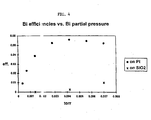
- Fig. 4 is a graphical representation on coordinates of bismuth triphenyl against deposition efficiency. It will be noted from the graph that bismuth oxide deposition occurs at a high rate upon a platinum substrate above a partial pressure of about 0.0025 torr (0.333Pa) whereas the deposition rate on silicon dioxide remains at a low level up to about 0.007 torr (0.933Pa). It is within this partial pressure window that selective deposition by chemical vapor deposition occurs.
- Fig. 1d Shown in Fig. 1d is the structure of Fig. 1c after the selective chemical vapor deposition of an SrBi 2 Ta 2 O 9 (SBT) top electrode layer 19 and a strontium tantalate layer 20 on top of the surrounding insulating material which is silicon dioxide or silicon nitride.
- SBT SrBi 2 Ta 2 O 9
- the resultant structure is subjected to a high temperature anneal in the presence of oxygen to transform the as-deposited phase to the ferroelectric Aurivillius phase.
- a high temperature anneal in the presence of oxygen to transform the as-deposited phase to the ferroelectric Aurivillius phase.
- the anneal is performed at a temperature from about 600-820°C, preferably 750-800°C.
- a top electrode 20a typically a noble metal electrode, is deposited upon the structure shown in Fig. 1d to yield the structure shown in Fig. 1e.
- a further high temperature anneal is effected in the presence of oxygen. This top electrode will then serve as the common plate for capacitors.
- the substrate chosen for use is a silicon dioxide matrix (TEOS) having a platinum electrode (1x1mm 2 ).
- TEOS silicon dioxide matrix
- the solvent employed was tetrahydrofurane/isopropanol/ tetraglyme in a ratio of 8:2:1.
- the concentrations of the precursors in this solvent system were about: 0.15 M Sr source, 0.4 M Ta source and 0.4 M Bi source.
- Each of the precursor solutions were stored separately and mixed prior to deposition. Following, the mixture of precursors was flash evaporated upon a matrix at a vaporization temperature of about 205°C with a liquid delivery rate ranging from about 0.05 to 0.2 ml/min. The vaporized precursors were then were then transported by an argon carrier gas to the reaction chamber. At the inlet of the chamber, the precursor stream was mixed further with argon and oxygen.
- the CVD reactor was a warm walled reactor (T wall is about 200°C) comprising a quartz tube having a diameter of about 12.5 cm. The substrate was arranged perpendicular to the gas flow and was heated to a temperature of about 620°C. Coating of the substrate was effected for 30 minutes. Following, the precursor delivery was stopped and the resultant structure permitted to cool in the argon/oxygen stream. Film thickness of the deposited film was approximately 80 nm.
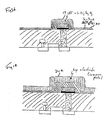
- Bi 2 O 3 is only deposited in those areas in which it is needed to form the ferroelectric SBT phase, namely on top of the bottom electrode.
- the insulating material that surrounds the bottom electrode is not covered with Bi 2 O 3 but instead covered only with SrO and Ta 2 O 5 .
- the significance of this finding is as follows. First, Bi 2 O 3 is known to react with SiO 2 to form bismuth silicates. Thus, if we have TEOS-SiO 2 beside the bottom electrode it would be transformed into a silicate. This will affect the stress in the entire wafer and increase the likelihood of the silicate density being different from that of TEOS-SiO 2 . Additionally, such a change in density might be accompanied by void formation.
- strontium and tantalum are deposited upon the silicon oxide surface, and the resultant strontium tantalum oxide layer is stable and will maintain excellent properties on the silica surface.
- the advantage of this selectivity is to reduce the number of processing steps required to form an integrated structure and to reduce the number of deposition processes required, particularly in light of the fact that it is likely that a unique material such as titania might be required to form a diffusion barrier in the absence of the selective process.
- Fig. 2a is a front elevational view in cross section of a silicon substrate 21 having deposited thereon an isolation dielectric 22, for example, silicon dioxide (SiO 2 )or silicon nitride (Si 3 N 4 ), which includes contact plug 23.
- isolation dielectric 22 for example, silicon dioxide (SiO 2 )or silicon nitride (Si 3 N 4 ), which includes contact plug 23.
- barrier layer 24 and bottom electrode 25 of the type described above;
- the next step in the process involves patterning the bottom electrode and barrier layer by conventional photolithographic techniques.
- the resultant structure is shown in Fig. 2b.
- an interlevel dielectric layer 26 is deposited upon the structure and patterned by conventional photolithographic techniques.
- a ferroelectric layer 27, shown in Fig. 2d is deposited selectively in the manner described above to yield a ferroelectric material over the bottom electrode 25 comprising SrBi 2 Ta 2 O 9 (SBT).
- SBT SrBi 2 Ta 2 O 9
- the layer 28 is not a ferroelectric and contains strontium and tantalum oxides which have excellent physical and chemical integrity and which does not require a barrier layer to prevent bismuth diffusion.
- Fig. 2e shows the structure of Fig. 2d after the deposition thereon of a top electrode 29 of the type described. When this layer is the common plate, the capacitor is complete. If desired the structure may be processed further by patterning the top electrode 29 by chemical mechanical polishing, as shown in Fig. 2f.
- the present invention may also be of interest in the fabrication of dissimilar capacitors in integrated circuits.
- ferroelectric SBT SrBi 2 Ta 2 O 9
- Figs. 3a-3e Shown in Fig 3a is a substrate member 31 having deposited thereon and patterned a platinum electrode 32.
- the next step in this process involves the selective deposition of SrBi 2 Ta 2 O 9 in accordance with the present invention.
- This results in the deposition of SBT films 33 on platinum electrodes 32 and a strontium tanatalate layer 34 on substrate 31 shown in Fig. 3b.
- a top electrode 35 typically platinum, is deposited upon the structure of Fig 3b to yield the structure of Fig. 3c.
- top electrode 35 is patterned to yield the structure of Fig. 3d.
- the cross-sectional figures 3a-3d are taken through section A-A of the top view of a device layout shown in Fig. 3e.
- non-ferroelectric capacitors may be formed intermediate to the lower electrode areas over a field oxide. This approach permits the fabrication in one oxide deposition step of dissimilar (ferroelectric and non-ferroelectric) capacitors.
- the ferroelectric capacitor cells can then be used for non-volatile memory while the non-ferroelectric capacitors will have inherently lower dielectric losses so that the non-ferroelectric capacitors can be used for other parts of the device system requiring lower dielectric losses.
- the described technique may be used in a procedure wherein the electrically conductive layer is part of a semiconductive device or part of the storage capacitor of a memory device.
- the technique may be employed in the fabrication of ferroelectric and non-ferroelectric capacitors on the same device.
Landscapes
- Chemical & Material Sciences (AREA)
- Organic Chemistry (AREA)
- Mechanical Engineering (AREA)
- Chemical Kinetics & Catalysis (AREA)
- Engineering & Computer Science (AREA)
- Materials Engineering (AREA)
- General Chemical & Material Sciences (AREA)
- Metallurgy (AREA)
- Inorganic Chemistry (AREA)
- Semiconductor Memories (AREA)
- Chemical Vapour Deposition (AREA)
- Inorganic Insulating Materials (AREA)
- Internal Circuitry In Semiconductor Integrated Circuit Devices (AREA)
- Formation Of Insulating Films (AREA)
Description
| Temperature (°C) | Pressure |
| 650-670 | 0.1-7.0 torr (0.1333x10²-9.3325x10²Pa) |
| 600-650 | 0.1-5.0 torr (0.1333x10²-6.666x10²Pa) |
| 550-600 | 0.1-2.0 torr (0.1333x10²-2.666x10²Pa) |
| 500-550 | 0.1-0.5 torr (0.1333x10²-0.666x10²Pa) |
Claims (27)
- A method for the selective deposition of a bismuth based ferroelectric film on a substrate member by metallorganic chemical vapor deposition comprising:placing a substrate member having insulating and electrically conductive surfaces in a chemical vapor deposition apparatus;heating the substrate to an elevated temperature within;exposing the substrate member to vaporized metallorganic precursors including a bismuth precursor carried by an inert gas into said apparatus and thermally decomposing said precursors for a time period sufficient to deposit a first thin metal oxide film on the electrically conductive surface and a second metal oxide film on the insulating surface, the electrically conductive surface and the insulating surface being chosen such that metal oxide film is deposited preferentially on the electrically conductive surface when exposed to such precursors;terminating the flow of precursors;subjecting the substrate and deposited layers to high temperature annealing in the presence of oxygen; andremoving the substrate from the apparatus.
- Method in accordance with claim 1 wherein the thermal decomposition is effected at a temperature within the range of 400-700°C.
- Method in accordance with claim 1 wherein the thermal decomposition is effected at a pressure ranging from 0.1 to 10 torr (0.133322x10²Pa to 1.33322x10³Pa).
- Method in accordance with claim 1 wherein the thermal decomposition is effected at a gas flow rate ranging from 100 to 20000 sccm.
- Method in accordance with claim 1 wherein said ferroelectric film is SrBi2Ta2O9 or derivatives thereof.
- Method in accordance with claim 1 wherein said ferroelectric film is Bi4Ti3O12 or derivatives thereof.
- Method in accordance with claim 1 wherein the precursors are generated by evaporation of solid or liquid compositions which are carried to the vapor deposition apparatus by an inert carrier gas.
- Method in accordance with claim 1 wherein the electrically conductive material is a noble metal selected from the. group consisting of platinum, palladium, rhodium, iridium, ruthenium, osmium and gold.
- Method in accordance with claim 8 wherein the noble metal is deposited upon a layer of insulating material.
- Method in accordance with claim 8 wherein the noble metal is deposited upon a layer of second conducting material.
- Method in accordance with claim 1 wherein the insulating material is silicon dioxide.
- Method in accordance with claim 1 wherein the insulating material is silicon nitride.
- Method in accordance with claim 10 wherein said second conducting material is selected from the group consisting of titanium, tantalum, tungsten and doped silicon.
- Method in accordance with claim 8 wherein the noble metal is deposited on a conducting barrier layer.
- Method in accordance with claim 1 wherein the bismuth precursor is selected from the group consisting of triphenyl bismuth, tritolyl bismuth, bismuth alkyl, bismuth alkoxides, bismuth carboxylates, bismuth b-diketonates, bismuth amides, mixed ligand bismuth compound and mixtures thereof.
- Method in accordance with claim 1 wherein the precursors comprise a mixture of strontium bis (β-diketonate), bismuth triphenyl and tantalum alkoxide β-diketonate.
- Method in accordance with claim 1 wherein the precursors comprise a mixture of Sr 2,2,5,5-tetramethylheptane-3,5-dionate as tetraglyme adduct, triphenyl bismuth and tantalum 2,2,5,5-tetramethylheptane-3,5-dionate tetrakis (isopropoxide).
- Method in accordance with claim 1 wherein the deposited ferroelectric film is SrBi2Ta2O9 which has been subjected to a high temperature anneal in the presence of oxygen at a temperature ranging from 600-820°C.
- Method in accordance with claim 1 wherein the substrate is heated to a temperature within the range of 650-670°C at a pressure within the range of 0.1-7.0 torr (0.133311x10²Pa-9.3325x10²Pa).
- Method in accordance with claim 1 wherein the substrate is heated to a temperature within the range of 600-650°C at a pressure within the range of 0.1-5.0 torr (0.1333x10²-6.666x10²Pa).
- Method in accordance with claim 1 wherein the substrate is heated to a temperature within the range of 550-600°C at a pressure within the range of 0.1-2.0 torr (0.1333x10²-2.666x10²Pa).
- Method in accordance with claim 1 wherein the substrate is heated to a temperature within the range of 500-550°C at a pressure within the range of 0.1-0.5 torr (0.1333x10²-0.666x10²Pa).
- Method in accordance with claim 1 wherein the precursor is delivered to the vapor deposition apparatus at a liquid delivery rate within the range of 0.05-1 milliliter per minute.
- Method in accordance with claim 23 wherein the precursor delivery rate ranges from 0.07 to 0.25 milliliters per minute.
- Method in accordance with claim 1 wherein the carrier gas flow ranges from 200-400 seem.
- Method in accordance with claim 18 wherein the SrBi2Ta2O9 ferroelectric film is deposited upon a platinum electrically conductive material and SrTaOx is deposited upon said insulating material.
- Method in accordance with claim 1 wherein another layer of a conductive material is deposited upon the chemical vapor deposited layer to form a capacitor.
Applications Claiming Priority (3)
| Application Number | Priority Date | Filing Date | Title |
|---|---|---|---|
| US08/996,575 US6120846A (en) | 1997-12-23 | 1997-12-23 | Method for the selective deposition of bismuth based ferroelectric thin films by chemical vapor deposition |
| US996575 | 1997-12-23 | ||
| PCT/US1998/026656 WO1999032685A1 (en) | 1997-12-23 | 1998-12-16 | Method for selectively depositing bismuth based ferroelectric films |
Publications (2)
| Publication Number | Publication Date |
|---|---|
| EP1042529A1 EP1042529A1 (en) | 2000-10-11 |
| EP1042529B1 true EP1042529B1 (en) | 2002-04-03 |
Family
ID=25543073
Family Applications (1)
| Application Number | Title | Priority Date | Filing Date |
|---|---|---|---|
| EP98963936A Expired - Lifetime EP1042529B1 (en) | 1997-12-23 | 1998-12-16 | Method for selectively depositing bismuth based ferroelectric films |
Country Status (7)
| Country | Link |
|---|---|
| US (1) | US6120846A (en) |
| EP (1) | EP1042529B1 (en) |
| JP (1) | JP2001527282A (en) |
| KR (1) | KR20010033553A (en) |
| CN (1) | CN1184348C (en) |
| DE (1) | DE69804672T2 (en) |
| WO (1) | WO1999032685A1 (en) |
Families Citing this family (37)
| Publication number | Priority date | Publication date | Assignee | Title |
|---|---|---|---|---|
| US6500489B1 (en) * | 1996-11-27 | 2002-12-31 | Advanced Technology Materials, Inc. | Low temperature CVD processes for preparing ferroelectric films using Bi alcoxides |
| US6693318B1 (en) * | 1997-12-18 | 2004-02-17 | Infineon Technologies North America | Reduced diffusion of a mobile specie from a metal oxide ceramic |
| JPH11186523A (en) * | 1997-12-19 | 1999-07-09 | Sharp Corp | Insulator material, insulating film-coated substrate, method for producing the same, and use thereof |
| WO2000034550A2 (en) * | 1998-12-09 | 2000-06-15 | Infineon Technologies Ag | Cvd processes using bi aryl |
| JP3664033B2 (en) * | 2000-03-29 | 2005-06-22 | セイコーエプソン株式会社 | Ceramic manufacturing method and manufacturing apparatus thereof |
| JP3596416B2 (en) * | 2000-03-29 | 2004-12-02 | セイコーエプソン株式会社 | Method for manufacturing ceramics and apparatus for manufacturing the same |
| KR100382149B1 (en) * | 2000-11-30 | 2003-05-09 | 한국전자통신연구원 | Formation method for Sr-Ta-O thin films |
| US7358121B2 (en) * | 2002-08-23 | 2008-04-15 | Intel Corporation | Tri-gate devices and methods of fabrication |
| US6798068B2 (en) * | 2002-11-26 | 2004-09-28 | Advanced Micro Devices, Inc. | MOCVD formation of Cu2S |
| US7118726B2 (en) | 2002-12-13 | 2006-10-10 | Clark Manufacturing, Llc | Method for making oxide compounds |
| KR100513724B1 (en) * | 2002-12-24 | 2005-09-08 | 삼성전자주식회사 | Ferroelectric thin film and preparing method thereof |
| JP2004256510A (en) * | 2003-02-26 | 2004-09-16 | Toyoshima Seisakusho:Kk | Bismuth raw material solution for CVD and method for producing bismuth-containing thin film using the same |
| US8478645B2 (en) * | 2003-04-07 | 2013-07-02 | Sevenecho, Llc | Method, system and software for digital media narrative personalization |
| US7456476B2 (en) | 2003-06-27 | 2008-11-25 | Intel Corporation | Nonplanar semiconductor device with partially or fully wrapped around gate electrode and methods of fabrication |
| US6909151B2 (en) * | 2003-06-27 | 2005-06-21 | Intel Corporation | Nonplanar device with stress incorporation layer and method of fabrication |
| JP4632018B2 (en) * | 2003-10-15 | 2011-02-16 | セイコーエプソン株式会社 | Ferroelectric film, method for manufacturing ferroelectric film, ferroelectric capacitor, and ferroelectric memory |
| US7154118B2 (en) | 2004-03-31 | 2006-12-26 | Intel Corporation | Bulk non-planar transistor having strained enhanced mobility and methods of fabrication |
| US7042009B2 (en) | 2004-06-30 | 2006-05-09 | Intel Corporation | High mobility tri-gate devices and methods of fabrication |
| US7348284B2 (en) | 2004-08-10 | 2008-03-25 | Intel Corporation | Non-planar pMOS structure with a strained channel region and an integrated strained CMOS flow |
| US7332439B2 (en) | 2004-09-29 | 2008-02-19 | Intel Corporation | Metal gate transistors with epitaxial source and drain regions |
| US7422946B2 (en) | 2004-09-29 | 2008-09-09 | Intel Corporation | Independently accessed double-gate and tri-gate transistors in same process flow |
| US20060086977A1 (en) | 2004-10-25 | 2006-04-27 | Uday Shah | Nonplanar device with thinned lower body portion and method of fabrication |
| US7518196B2 (en) | 2005-02-23 | 2009-04-14 | Intel Corporation | Field effect transistor with narrow bandgap source and drain regions and method of fabrication |
| US20060202266A1 (en) | 2005-03-14 | 2006-09-14 | Marko Radosavljevic | Field effect transistor with metal source/drain regions |
| JP4257537B2 (en) * | 2005-06-02 | 2009-04-22 | セイコーエプソン株式会社 | Ferroelectric layer manufacturing method, electronic device manufacturing method, ferroelectric memory device manufacturing method, piezoelectric element manufacturing method, and ink jet recording head manufacturing method |
| US7858481B2 (en) | 2005-06-15 | 2010-12-28 | Intel Corporation | Method for fabricating transistor with thinned channel |
| US7547637B2 (en) | 2005-06-21 | 2009-06-16 | Intel Corporation | Methods for patterning a semiconductor film |
| US7279375B2 (en) | 2005-06-30 | 2007-10-09 | Intel Corporation | Block contact architectures for nanoscale channel transistors |
| US7402875B2 (en) | 2005-08-17 | 2008-07-22 | Intel Corporation | Lateral undercut of metal gate in SOI device |
| US7479421B2 (en) | 2005-09-28 | 2009-01-20 | Intel Corporation | Process for integrating planar and non-planar CMOS transistors on a bulk substrate and article made thereby |
| US20070090416A1 (en) | 2005-09-28 | 2007-04-26 | Doyle Brian S | CMOS devices with a single work function gate electrode and method of fabrication |
| CN1967749B (en) * | 2005-11-18 | 2010-05-12 | 同济大学 | A low-temperature preparation method of non-lead ferroelectric thin film |
| US7485503B2 (en) | 2005-11-30 | 2009-02-03 | Intel Corporation | Dielectric interface for group III-V semiconductor device |
| US8143646B2 (en) | 2006-08-02 | 2012-03-27 | Intel Corporation | Stacking fault and twin blocking barrier for integrating III-V on Si |
| US8362566B2 (en) | 2008-06-23 | 2013-01-29 | Intel Corporation | Stress in trigate devices using complimentary gate fill materials |
| ITRM20120478A1 (en) | 2012-10-09 | 2014-04-10 | Sicurezza E Ambiente S P A | POLYFUNCTIONAL TRUCK PERFECTED ACTIVATED FOR CLEANING AREAS INTERESTED BY ROAD ACCIDENTS FOR RAPID RESTORATION OF ROADSHIP AND ROAD SAFETY |
| CN107619284B (en) * | 2017-09-08 | 2020-08-04 | 东华大学 | Preparation method of SiBNC ceramic foam |
Family Cites Families (6)
| Publication number | Priority date | Publication date | Assignee | Title |
|---|---|---|---|---|
| US5217756A (en) * | 1990-06-08 | 1993-06-08 | Nec Corporation | Selective chemical vapor deposition of aluminum, aluminum CVD materials and process for preparing the same |
| DE4038990C1 (en) * | 1990-12-06 | 1992-04-09 | Siemens Ag, 8000 Muenchen, De | |
| JPH07224385A (en) * | 1994-02-09 | 1995-08-22 | Fujitsu Ltd | Metal thin film selective vapor deposition method |
| US5478610A (en) * | 1994-09-02 | 1995-12-26 | Ceram Incorporated | Metalorganic chemical vapor deposition of layered structure oxides |
| US5527567A (en) * | 1994-09-02 | 1996-06-18 | Ceram Incorporated | Metalorganic chemical vapor deposition of layered structure oxides |
| JP3363301B2 (en) * | 1995-03-08 | 2003-01-08 | シャープ株式会社 | Ferroelectric thin film-coated substrate, method of manufacturing the same, and nonvolatile memory constituted by ferroelectric thin-film-coated substrate |
-
1997
- 1997-12-23 US US08/996,575 patent/US6120846A/en not_active Expired - Lifetime
-
1998
- 1998-12-16 CN CNB988137747A patent/CN1184348C/en not_active Expired - Fee Related
- 1998-12-16 EP EP98963936A patent/EP1042529B1/en not_active Expired - Lifetime
- 1998-12-16 WO PCT/US1998/026656 patent/WO1999032685A1/en not_active Ceased
- 1998-12-16 DE DE69804672T patent/DE69804672T2/en not_active Expired - Fee Related
- 1998-12-16 JP JP2000525598A patent/JP2001527282A/en not_active Withdrawn
- 1998-12-16 KR KR1020007007062A patent/KR20010033553A/en not_active Ceased
Also Published As
| Publication number | Publication date |
|---|---|
| DE69804672T2 (en) | 2002-10-10 |
| US6120846A (en) | 2000-09-19 |
| JP2001527282A (en) | 2001-12-25 |
| CN1184348C (en) | 2005-01-12 |
| DE69804672D1 (en) | 2002-05-08 |
| CN1285007A (en) | 2001-02-21 |
| WO1999032685A1 (en) | 1999-07-01 |
| EP1042529A1 (en) | 2000-10-11 |
| KR20010033553A (en) | 2001-04-25 |
Similar Documents
| Publication | Publication Date | Title |
|---|---|---|
| US6120846A (en) | Method for the selective deposition of bismuth based ferroelectric thin films by chemical vapor deposition | |
| US6010744A (en) | Method for nucleation controlled chemical vapor deposition of metal oxide ferroelectric thin films | |
| KR100472258B1 (en) | Single transistor ferroelectric transistor structure with high-k insulator and method of fabricating same | |
| EP1212476B1 (en) | Dielectric films and methods of forming same | |
| EP1368822B1 (en) | Rhodium-rich oxygen barriers | |
| US6806183B2 (en) | Methods for forming capacitors on semiconductor substrates | |
| JP3909753B2 (en) | Ferroelectric transistor structure and manufacturing method thereof | |
| US6133051A (en) | Amorphously deposited metal oxide ceramic films | |
| US20070014919A1 (en) | Atomic layer deposition of noble metal oxides | |
| US7259058B2 (en) | Fabricating method of semiconductor integrated circuits | |
| JPH0927602A (en) | Capacitor and method for manufacturing high-capacity capacitor | |
| JP3803583B2 (en) | High-speed lamp annealing method for manufacturing superlattice materials | |
| US20040101977A1 (en) | Low thermal budget fabrication of ferroelectric memory using RTP | |
| US6544857B1 (en) | Dielectric capacitor manufacturing method and semiconductor storage device manufacturing method | |
| US6376299B1 (en) | Capacitor for semiconductor memory device and method of manufacturing the same | |
| JP2003512715A (en) | Low temperature CVD method for forming ferroelectric film using Bi alkoxide | |
| US6756261B2 (en) | Method for fabricating capacitors in semiconductor devices | |
| KR100238249B1 (en) | Fabrication method of high dielectric capacitor | |
| US20040023416A1 (en) | Method for forming a paraelectric semiconductor device | |
| KR100395507B1 (en) | Semiconductor device and the method of fabricating same | |
| KR100265846B1 (en) | A method for fabricating ferroelectric capacitor in semiconductor device | |
| JP4330907B2 (en) | Method for manufacturing metal oxide film and method for manufacturing capacitor element | |
| KR20080038713A (en) | Capacitor manufacturing method using atomic layer deposition | |
| KR20030084331A (en) | Method for fabricating capacitor with 2 step annealing in semiconductor device | |
| KR20040060416A (en) | Method for fabricating capacitor of semiconductor device |
Legal Events
| Date | Code | Title | Description |
|---|---|---|---|
| PUAI | Public reference made under article 153(3) epc to a published international application that has entered the european phase |
Free format text: ORIGINAL CODE: 0009012 |
|
| 17P | Request for examination filed |
Effective date: 20000712 |
|
| AK | Designated contracting states |
Kind code of ref document: A1 Designated state(s): DE FR GB IE IT |
|
| RIN1 | Information on inventor provided before grant (corrected) |
Inventor name: BAUM, THOMAS, H. Inventor name: VAN BUSKIRK, PETER Inventor name: ROEDER, JEFFREY, R. Inventor name: HENDRIX, BRYAN Inventor name: HINTERMAIER, FRANK |
|
| GRAG | Despatch of communication of intention to grant |
Free format text: ORIGINAL CODE: EPIDOS AGRA |
|
| 17Q | First examination report despatched |
Effective date: 20010202 |
|
| GRAG | Despatch of communication of intention to grant |
Free format text: ORIGINAL CODE: EPIDOS AGRA |
|
| GRAH | Despatch of communication of intention to grant a patent |
Free format text: ORIGINAL CODE: EPIDOS IGRA |
|
| GRAH | Despatch of communication of intention to grant a patent |
Free format text: ORIGINAL CODE: EPIDOS IGRA |
|
| REG | Reference to a national code |
Ref country code: GB Ref legal event code: IF02 |
|
| GRAA | (expected) grant |
Free format text: ORIGINAL CODE: 0009210 |
|
| AK | Designated contracting states |
Kind code of ref document: B1 Designated state(s): DE FR GB IE IT |
|
| REF | Corresponds to: |
Ref document number: 69804672 Country of ref document: DE Date of ref document: 20020508 |
|
| REG | Reference to a national code |
Ref country code: IE Ref legal event code: FG4D |
|
| PLBE | No opposition filed within time limit |
Free format text: ORIGINAL CODE: 0009261 |
|
| STAA | Information on the status of an ep patent application or granted ep patent |
Free format text: STATUS: NO OPPOSITION FILED WITHIN TIME LIMIT |
|
| 26N | No opposition filed |
Effective date: 20030106 |
|
| PGFP | Annual fee paid to national office [announced via postgrant information from national office to epo] |
Ref country code: IT Payment date: 20071221 Year of fee payment: 10 |
|
| PGFP | Annual fee paid to national office [announced via postgrant information from national office to epo] |
Ref country code: DE Payment date: 20080213 Year of fee payment: 10 |
|
| PGFP | Annual fee paid to national office [announced via postgrant information from national office to epo] |
Ref country code: FR Payment date: 20071217 Year of fee payment: 10 |
|
| REG | Reference to a national code |
Ref country code: GB Ref legal event code: 732E |
|
| PGFP | Annual fee paid to national office [announced via postgrant information from national office to epo] |
Ref country code: GB Payment date: 20081210 Year of fee payment: 11 |
|
| PGFP | Annual fee paid to national office [announced via postgrant information from national office to epo] |
Ref country code: IE Payment date: 20071220 Year of fee payment: 10 |
|
| REG | Reference to a national code |
Ref country code: IE Ref legal event code: MM4A |
|
| REG | Reference to a national code |
Ref country code: FR Ref legal event code: ST Effective date: 20090831 |
|
| PG25 | Lapsed in a contracting state [announced via postgrant information from national office to epo] |
Ref country code: IE Free format text: LAPSE BECAUSE OF NON-PAYMENT OF DUE FEES Effective date: 20081216 Ref country code: DE Free format text: LAPSE BECAUSE OF NON-PAYMENT OF DUE FEES Effective date: 20090701 |
|
| PG25 | Lapsed in a contracting state [announced via postgrant information from national office to epo] |
Ref country code: FR Free format text: LAPSE BECAUSE OF NON-PAYMENT OF DUE FEES Effective date: 20081231 |
|
| GBPC | Gb: european patent ceased through non-payment of renewal fee |
Effective date: 20091216 |
|
| PG25 | Lapsed in a contracting state [announced via postgrant information from national office to epo] |
Ref country code: GB Free format text: LAPSE BECAUSE OF NON-PAYMENT OF DUE FEES Effective date: 20091216 |
|
| PG25 | Lapsed in a contracting state [announced via postgrant information from national office to epo] |
Ref country code: IT Free format text: LAPSE BECAUSE OF NON-PAYMENT OF DUE FEES Effective date: 20081216 |