EP1041718A2 - A low power adjustable input threshold circuit - Google Patents
A low power adjustable input threshold circuit Download PDFInfo
- Publication number
- EP1041718A2 EP1041718A2 EP00105976A EP00105976A EP1041718A2 EP 1041718 A2 EP1041718 A2 EP 1041718A2 EP 00105976 A EP00105976 A EP 00105976A EP 00105976 A EP00105976 A EP 00105976A EP 1041718 A2 EP1041718 A2 EP 1041718A2
- Authority
- EP
- European Patent Office
- Prior art keywords
- transistors
- comparator
- pair
- voltage
- signal
- Prior art date
- Legal status (The legal status is an assumption and is not a legal conclusion. Google has not performed a legal analysis and makes no representation as to the accuracy of the status listed.)
- Granted
Links
Images




Classifications
-
- H—ELECTRICITY
- H03—ELECTRONIC CIRCUITRY
- H03K—PULSE TECHNIQUE
- H03K17/00—Electronic switching or gating, i.e. not by contact-making and –breaking
- H03K17/30—Modifications for providing a predetermined threshold before switching
- H03K17/302—Modifications for providing a predetermined threshold before switching in field-effect transistor switches
Definitions
- the invention relates to voltage comparators, and more particularly relates to establishing voltage comparator input threshold control.
- Voltage comparators are used in electronic systems to detect that a signal of interest has attained some predetermined value which is commonly referred to as the threshold level. When this event occurs the comparator produces a change in logic level at its output to indicate the threshold level has been attained.
- the threshold detection function of a voltage comparator is typically accomplished by electronically comparing the signal of interest to an externally supplied reference voltage.
- An example of an application of a voltage comparator is the detection that a primary power supply voltage has exceeded specification limits, thereby warranting a corrective action of some sort, such as system shutdown.
- Another application is the detection of the presence or absence of a data transmission cable, through a bias voltage present in the cable when connected, to begin or halt data transmission or reception, or otherwise indicate the connection status of the cable.
- the threshold detection function of a voltage comparator is typically accomplished by electronically comparing the signal of interest to an externally supplied reference voltage.
- the primary technical issues associated with the use of a voltage comparator are precision of the external reference power supply, accuracy of the electronic comparison, and power requirements of the included components.
- the complexity of the comparator implementation therefore varies between wide extremes depending upon the specific application and associated requirements.
- setting and controlling the threshold level for the comparator is the main contributor to complexity and power consumption due to the necessity for a reference power supply that typically must remain powered on during system operation.
- a further requirement of a comparator is that it must produce a change in logic state at its output that corresponds to the signal of interest having attained the threshold level in both positive and negative going directions. For example, if the comparator output is at a logic "1" when the signal of interest is below the threshold level, the output must change to a logic "0” and remain there when the threshold level is reached or exceeded. Also, for this example, the comparator output must change from a logic "0” to a logic "1” and remain there when the signal of interest falls below the threshold level.
- the simplest approach to accomplishing the comparator function is through the use of a simple inverter as shown in Figure 1.
- the signal of interest V IN is applied to the input of inverter 10, and upon reaching the threshold level of the input gate of a semiconductor device within the inverter 10, causes the output of inverter 10 to change logic states.
- the threshold level is determined by the particular device used to form the input gate, the power supply voltage, and operating temperature. This approach has very low power requirements, but does not provide a means of adjusting the threshold level. Nor does it provide the accuracy required of most comparator applications in determining that the threshold level has been reached.
- Figure 2 illustrates a differential comparator circuit wherein V OUT will change logic states when the signal of interest, Vin, equals or exceeds the threshold level, Vth.
- the threshold level for the comparator is established through use of an external precision reference power supply 14 as the second input to the comparator. This approach is often enhanced to achieve improved performance by adding circuitry for temperature compensation and reducing power supply drift, but with a penalty of increased power consumption and complexity.
- Figure 3 also shows a differential comparator, but with the addition of a digital to analog converter, (“DAC") 18, used in conjunction with an external reference supply 20 for setting the threshold level, Vth.
- the threshold level is set by means of a serial programming bus 22 to the DAC 18, and may be changed as the specific application or operating conditions may dictate. This approach offers substantially improved threshold level accuracy, but with increased power consumption and complexity, over that achievable with the examples described above.
- a variable threshold comparator receiving, on an input node, an input signal having a voltage, and providing an output signal on an output node when the voltage of the input signal exceeds a selectable threshold voltage of the comparator.
- the comparator includes a transistor coupled by way of its source and drain between a first polarity power supply node and an output node, and having its gate coupled to the input node.
- the threshold voltage of the comparator is selectable by the application of one or more of the control signals to a respective one or more of the second ones of said transistors.
- a variable threshold comparator receiving, on an input node, an input signal having a voltage, and providing an output signal on an output node when the voltage of the input signal exceeds a selectable threshold voltage of the comparator.
- the comparator includes a first plurality of pairs of transistors, each pair, denominated the first pair, in the first plurality of pairs of transistors being coupled together by a source of a first one of the first pair of transistors and a drain of a second one of the first pair of transistors, and coupled in series between the output node and a first polarity power supply node.
- a gate of the first one of the first pair of transistors is coupled to the input node, and a gate of the second one of the first pair of transistors is coupled to a control signal specific to the second one of the first pair of the transistors.
- a second plurality of pairs of transistors is also included, each pair, denominated the second pair, in the second plurality of pairs of transistors being coupled together by a source of a first one of the second pair of transistors and a drain of a second one of the second pair of transistors, and coupled in series between the output node and a second polarity power supply node.
- a gate of the first one of the second pair of transistors is coupled to the input node, and a gate of the second one of the second pair of transistors is coupled to a control signal specific to the second one of the second pair of transistors.
- the threshold voltage of the comparator is selectable by the application of one or more of the control signals to a respective one or more of the second ones of the transistors.
- the preferred embodiment of the present invention is disclosed herein in the context of its use in a semiconductor device known as a Cable Transceiver/Arbiter, as defined by IEEE Standard 1394 which delineates the performance requirements for the analog and digital physical layer functions for a high performance serial data bus.
- the preferred embodiment performs the function commonly referred to as Cable Not Active (CNA), and in so doing includes means to detect the connection status of a data transmission cable and indicate that status to the control logic of the semiconductor device.
- CNA Cable Not Active
- the preferred embodiment significantly reduces power consumption in performing a voltage comparator-type function, and also significantly reduces the propagation delay time of the change in output logic level, when compared to that of the prior art.
- the preferred embodiment includes means for performing an electronic comparison of the signal of interest to a predetermined reference or threshold value. It will further be seen that the preferred embodiment provides a logic level output signal whenever the signal of interest has equaled or exceeded this threshold value in both positive and negative going directions.
- the threshold level for the aforementioned electronic comparison is realized by the inclusion of circuit elements in a cascade configuration comprised of transistors with appropriately different conduction channel dimensions. It will be seen the preferred embodiment includes means for adjusting the threshold level of a comparator circuit through application of externally supplied fixed control voltages to the cascaded elements, as might be necessary to compensate for variations in device process, operating temperature, power supply voltage, or other operating conditions.
- the preferred embodiment is readily expandable or contractible by the addition or deletion of almost identical circuit elements to the cascade configuration, the difference in these circuit elements being only individual transistor conduction channel dimensions. It will be seen the preferred embodiment is thus able to accommodate the selection of different threshold levels for the signal of interest as specific application requirements may dictate.
- the preferred embodiment includes means for selecting the desired degree of precision for the aforementioned electronic comparison also through the addition or deletion of circuit elements to the cascade configuration. These circuit elements too would differ only in individual transistor conduction channel dimensions.
- threshold level for an individual transistor is that voltage at which the transistor is placed in, or removed from, a conductive state by application of the voltage to the transistor gate.
- threshold value or “threshold level” when applicable to the signal of interest is denoted as "Vth”
- Vt voltage at which the transistor is placed in, or removed from, a conductive state by application of the voltage to the transistor gate.
- the MOS transistor can be empirically characterized as an almost linear device wherein the drain current is proportional to the voltage applied to the transistor gate for fixed values of threshold voltage (Vt), source-to-drain voltage, channel width, and channel length. Further, the conductance of a MOS transistor is proportional to the device channel width and length for fixed device-peculiar parameters that are dependent upon materials content and manufacturing process. The conductance of a MOS transistor, or, inversely, its resistivity, is also determined by its threshold voltage and the voltage applied to its gate, for some given dimensions of the conduction channel.
- Figure 4 is a schematic diagram of a portion 24 of a voltage comparator, in accordance with the preferred embodiment of the present invention.
- Figure 4 shows an inverter circuit comprised of transistors T1 and T2, and a transistor T3 in the configuration of a control gate.
- Figure 4 is discussed to illustrate basic principles of circuit operation. It is shown below that the circuit branch of Figure 4 comprised of transistors T2 and T3 is but one branch of a cascade configuration of a more expanded comparator 30, shown in Figure 5.
- the conduction states of transistors T1 and T2 are determined by input voltage Vin on signal line 26 and the respective threshold voltages Vt for the transistors; the conduction state of transistor T3 is determined by its threshold Vt voltage and input voltage Vc.
- transistors T1 and T2 behave as a simple inverter. As such, a positive going voltage for Vin causes transistor T2 to conduct more heavily and also causes transistor T1 to conduct less. Consequently, output voltage V OUT on signal line 28 approaches ground potential for a positive going input voltage Vin. Conversely, a negative going input voltage Vin causes transistor T1 to conduct more heavily and transistor T2 to conduct less, causing output voltage V OUT to approach V DD .
- FIG. 5 shows the complete schematic of the voltage comparator of the preferred embodiment of the present invention with Vin on signal line 26 being the signal of interest as an input, V OUT on signal line 28 being an output logic signal, and signals Vc1 through VcN being externally supplied fixed control voltages. It is described in detail below that output signal V OUT changes logic state whenever input signal Vin attains some predetermined threshold (Vth) level in both positive and negative going directions, as is the case for a typical differential comparator circuit.
- Vth threshold
- Control voltages Vc1 through VcN are externally supplied. Possible sources and characteristics of voltages Vc1 through VcN are discussed in more detail below. Further, the means by which voltages Vc1 through VcN are supplied to the circuit of comparator 30 may vary as a function of the specific application.
- circuit of comparator 30 shown in Figure 5 is an expansion of the circuit portion 24 shown in Figure 4.
- circuit branch of Figure 4 comprised of transistors T2 and T3 is replicated in a cascade configuration as represented by transistors T4 through T9 in Figure 5.
- Transistors T1 through T3 in Figure 5 are similar to or the same as those in Figure 4.
- Circuit branch N of Figure 5 is shown to indicate that any number of branches may be included in the cascade configuration.
- the number of circuit branches used will be determined by the degree of precision required in performing the threshold (Vth) detection function and the threshold (Vth) level required for the comparator, as dictated by the specific application requirements.
- the means by which improved precision is achieved and the threshold (Vth) level is set is presented below.
- Figure 6 is a partial equivalent circuit of the comparator of Figure 5 and is made up of the effective resistivities of transistors T1 through T9, represented by R1 through R9, respectively.
- the resistivity of a MOS transistor is a function of the conduction state of the transistor which will vary with gate voltage for a given threshold (Vt) voltage and conduction channel dimensions, in accordance with the empirical characterization presented earlier.
- V OUT V DD *(RE)/(R1+RE), where:
- transistor T1 a PMOS transistor
- resistivities of transistors T2 through T9 all NMOS transistors
- the resistivity of transistor T1 will decrease and the resistivities of transistors T2 through T9 will increase for a decrease in the respective gate voltage.
- the voltage V OUT is determined by the gate voltage applied to transistors T1 through T9 and their respective resistivities. As such, the voltage V OUT , for some Vin, can be made to approach ground potential by decreasing the effective resistivity between signal line 28 and ground, which is accomplished by placing transistors T2 through T9 in a conductive state. V OUT can be made to approach V DD by increasing the effective resistivity between signal line 28 and ground, which is accomplished by placing transistors T2 through T9 in a non-conductive state. Output voltage V OUT can therefore be made to respond to Vin by causing transistors T2 through T9 to be placed in conductive or non-conductive states in some logical order until the desired V OUT is obtained.
- the conduction states of transistors T2 through T9 are also determined by control voltages Vc1 through Vc4.
- the circuit of Figure 5 can be made to behave as an inverter having a threshold voltage controllable by appropriate selection of these control voltages.
- Transistors T2, T4, T6, and T8 in Figure 5, as a group are constructed such that they exhibit successively higher values of conductance by varying the dimensions of their respective conduction channels.
- transistors T3, T5, T7, and T9 are constructed with the same properties, also as a group.
- the specific conductance values of the two groups are not necessarily the same.
- Transistors T2, T4, T6, and T8 are those in the branch circuits of Figure 5 to whose gates the signal of interest Vin is applied.
- the use of transistors with successively increasing values of conductance provides an incremental control of the effective resistivity between signal line 28 and ground of Figure 5. Therefore, the response of output voltage V OUT to input voltage Vin is determined incrementally by the conduction state of transistor T1, as determined by Vin, and the conduction states of the branch circuit transistors which is also determined by Vin and the control voltages Vc1 through Vc4.
- Comparator 30 is thus able to accommodate any threshold (Vth) level that may be required for a signal of interest through the appropriate selection of the individual transistor conduction channel dimensions and the number of branch circuits used.
- Vth threshold
- the comparator circuit of the preferred embodiment of the present invention includes five branch circuits, one of which is kept in a conductive state at all times. This permits the selection of up to sixteen combinations of conduction states of the branch circuits and establishes a maximum value for the threshold (Vth) of the comparator. The remaining four branches may be placed in either a conductive or non-conductive state, providing up to sixteen increments of selection for the threshold (Vth) level between the minimum and maximum values of the signal of interest.
- Figure 7 shows a comparator 30' similar to comparator 30 of Figure 5.
- a single PMOS transistor T1 is coupled between V DD and V OUT
- a single NMOS transistor T1' is coupled between ground and V OUT .
- the gate of transistor T1' is connected to V IN .
- the NMOS transistors T2 - T9 of Figure 5 coupled between V OUT and ground are replaced in Figure 6 with PMOS transistors T2' - T9' coupled between V OUT and V DD .
- Control voltages Vc1 through Vc4 are connected to the gates of transistors T3', T5', T7' and T9', and V IN is connected to the gates of T2', T4', T6' and T8'.
- Branch N' is shown to illustrate that an improvement in precision can be achieved by increasing the number of branch circuits as desired.
- comparator 30' of Figure 6 Operation of the comparator 30' of Figure 6 is similar to that of comparator 30 of Figure 5, as well, the difference between the two circuits being, essentially, that opposite conductivity devices are used, and the polarity of the required power supply connections are consequently reversed. Considerations of varying the threshold voltages of the branch transistors T2' - T8' and procedures for adjustment of the threshold voltage of the comparator 30' are essentially the same as those for comparator 30 of Figure 5.
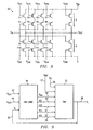
- FIG 8. Another exemplary comparator 30'' is shown in Figure 8.
- four branch circuits comprising PMOS transistors F1 - F8 are shown, that are similar to the four branch circuits comprising PMOS transistors T2' - T8' of Figure 7, being controlled by control voltages V CP1 - V CP4 , respectively.
- four branch circuits comprising NMOS transistors F9 - F16 are shown, that are similar to the four branch circuits comprising PMOS transistors T2 - T8 of Figure 5, being controlled by control voltages V CN1 -V CN4 , respectively.
- Branch S is shown to illustrate that an improvement in precision can be achieved by increasing the number of PMOS branch circuits as desired
- branch R is shown to illustrate that an improvement in precision can also be achieved by increasing the number of NMOS branch circuits as desired.
- Control voltages V CP1 through V CP4 are connected to the gates of transistors F1, F3, F5 and F7, while control voltages V CN1 through V CN4 are connected to the gates of transistors F10, F12, F14 and F16.
- Operation of the comparator 30'' essentially combines the principles of operation of comparator 30 ( Figure 5) and of comparator 30' ( Figure 7). Considerations of varying the threshold voltages of the branch transistors F1 - F16, and procedures for adjustment of the threshold voltage of the comparator 30'' are essentially the same as those for comparators 30 and 30' of Figures 5 and 7, respectively, with no preference to NMOS transistors over PMOS transistors, nor vice versa, in considerations of setting of threshold voltage for a particular transistor, nor in selection of transistor for actual comparator threshold voltage adjustment. The threshold voltages for all transistors are simply all available for setting and selection to provide comparator threshold adjustability, as desired.
- control voltages Vc1 through VcN in Figure 5 may vary according to the specific application.
- the only constraints placed on these control voltages is that they be appropriate for the threshold (Vt) level for the transistors to which they are applied and remain fixed.
- the control voltages are to be selected so as to place the respective branch transistors in either a conductive or non-conductive state, dependent upon the threshold (Vth) of the signal of interest and degree of precision required, as dictated by the specific application requirements.
- the control voltages may be selected through some digital means or other circuitry means as deemed appropriate for the specific application.
- FIG. 9 is a partial functional block diagram of an application of the preferred embodiment.
- Block 32 labeled CNA
- block 34 labeled CNA Logic
- FIG. 9 also shows signal V SI on signal line 36 which is the signal of interest for the preferred embodiment, and signal V L on signal line 38 which is the logic signal which changes state whenever signal V SI has attained a predetermined threshold (Vth) value.
- signal V REF is a fixed reference voltage; signals V CLK and V CLR are clock and clear signals, respectively, utilized by flipflop devices (described below) within CNA Logic 34 for performing the periodic calibration/adjustment cycle.
- FIG. 9 shows also signals Vc1 through Vc4 on signal lines 50 through 53, respectively, which are the fixed control voltages for the comparator circuit of Figure 5. Also shown is signal V CAL on signal line 46 which is supplied by CNA Logic 34 to CNA 32 for use in performing a periodic calibration/adjustment cycle.
- CNA Logic 34 includes the means to perform a periodic calibration/adjustment of the comparator circuit of Figure 5 included in CNA 32 whenever signals V CLK and V CLR are active. This is discussed in more detail below.
- CNA Logic 34 also includes the means to cause signal V REF to be substituted for signal V SI within CNA 32, and also the means to detect the logic level of output signal V L .
- CNA Logic 34 also includes the means to change the value of control voltages Vc1 through Vc4 in response to signal V L .
- CNA 32 also includes the means to substitute signal V REF in place of signal V SI , whenever signal V CAL is active. This is also discussed in more detail below.
- the periodic calibration/adjustment cycle can be summarized as follows: whenever signals V CLK and V CLR are active V CAL from CNA Logic 34 causes CNA 32 to substitute V REF for V SI as the signal of interest to the comparator circuit. Output signal V L is monitored by CNA Logic 34, which sequentially changes the values of control voltages Vc1 through Vc4 until an appropriate change occurs in the logic level of signal V L . CNA Logic 34, again via signal V CAL , then causes V SI to be reinstated as the signal of interest to the comparator circuit in CNA 32; control voltages Vc1 through Vc4 are kept at the values realized when V L changed logic state.
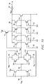
- Figure 10 is a schematic diagram of the circuitry of CNA 32 in Figure 9 comprised of the adjustable input threshold (Vth) control circuit.
- Figure 10 includes the comparator circuit of Figure 5 described previously, comprised of transistors T1 through T9, and signal V OUT as an input to inverter 60, whose output is logic signal V L on signal line 38. Also shown are input signals V SI , V REF , and V CAL on signal lines 36, 40, and 46, respectively, corresponding to those of Figure 9.
- transistor T10 which serves to enhance the precision of the electronic comparison by establishing a maximum value for the threshold (Vth) level of the comparator; otherwise, the comparator circuit functions as described previously.
- Input signal V CAL is normally at a logic level high, causing transistor T15 to be off and transistor T16 to be on, further causing signal line 62 to approach ground potential. This in turn causes transistors T22 and T23 to be in conductive states, and transistors T20 and T21 to be in non-conductive states, allowing signal V SI to be passed to signal line 26 as signal Vin to the comparator.
- each of the transistor pairs T20/T21 and T22/T23 are transmission gates.
- control voltages Vc1 through Vc4 in Figure 10 on signal lines 50 through 53, respectively, are selected by CNA Logic 34 of Figure 9 during the calibration/adjustment cycle so as to cause an appropriate change in output signal V L , corresponding to the substituted signal of interest V REF being at the required threshold (Vth) level.
- Figure 11 is a logic diagram for CNA Logic 34 shown in Figure 9. It performs the aforementioned calibration/adjustment cycle in order to select the appropriate control voltages that set the threshold (Vth) level for the comparator circuit of Figure 10. It should be noted that it is possible to design embodiments other than that shown in Figure 11 to perform the calibration/adjustment cycle, or otherwise select the control voltages that set the threshold (Vth) level, using the principles of the present invention disclosed herein.
- Figure 12, below shows, for example, an alternative embodiment of CNA Logic 34.
- the CNA Logic 34 of Figure 11 includes flipflops 70 through 78 which are enabled D positive edge triggered flipflops with a clear input. Note that the clear input logic is negative, as shown by the bar over the label for the clear input, i.e., CLR . Note also that the output is provided in positive logic, i.e., Q, and negative logic, i.e., Q .
- V CLR on signal line 44 is active high long enough to place the Q output of each flipflop at a logic low, via signal line 80.
- input clock signal V CLK is supplied as an input to NOR gate 82.
- signal V CAL which is low, and the output signal from AND gate 84, via signal line 86, which is also low by virtue of signals Vc1 through Vc4 being low.
- NOR gate 82 is thus able to provide clock signal V CLK to each flipflop via signal line 88. Also at this time input signal V L from CNA of Figure 10 is low.
- the Q output of flipflop 72 Upon receipt of clock signal V CLK the Q output of flipflop 72 goes high by virtue of its Q output being high, since this Q output is provided as the D input on signal line 90.
- the Q outputs of flipflops 74, 76, and 78 also go high, sequentially, as determined by the clock-triggering of each and the output state of exclusive-or gates 92, 94, and 96, which provide the respective D inputs.
- the circuit of Figure 11 functions as a binary counter responding to signal V CLK , in that the control voltages Vc1 through Vc4 are selected in an up-counting sequence until the calibration/adjustment cycle is terminated. The circuit is therefore able to select up to sixteen possible combinations of the control voltages.
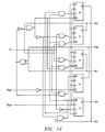
- Figure 12 is a logic diagram of an alternative embodiment, logic block 98, for the CNA Logic 34 shown in Figure 9.
- Logic block 98 utilizes enabled D positive edge triggered flipflops, as well as other conventional logic devices interconnected as shown in Figure 12.
- the three flipflops at the top of the figure have a preset input, while the two flipflops at the bottom of the figure have a clear input.
- the logic block 98 generates a sequence of patterns for the activation of the control signals Vc1 - Vc4, wherein the control signals correspond to a 4-bit binary count.
- the logic block 98 is wired to the CNA block 32 such that an incremental increase in that binary count causes an incremental decrease in the threshold level of the comparator 30 in CNA block 32.
- the pattern actually generated by logic block 98 is such that the CNA block 32 is initially tested at an intermediate binary count. Depending on the state of V L , the next binary jump is either up or down. If V L is low, the count jump is to a higher value. On the other hand, if V L is high, the count jump is to a lower value. By making each such jump approximately half of the remaining range, the final value is arrived at in the minimum number of jumps.
- the logic in block 98 When V L finally changes in response to a single binary increment, then the logic in block 98 either simply stops and holds the then current pattern of control signals, in the case of a single positive binary increment, or, in the case of a single negative binary increment, the logic block 98 changes the binary pattern of control signals so as to advance the binary count up by one increment, and then holds that pattern.
- the logic in block 98 can result in a fewer number of patterns being tested before the desired threshold is achieved.
- Figure 13 is a partial functional block diagram of assignee's proprietary IEEE 1394 compliant Cable Transceiver/Arbiter semiconductor device 100. This figure depicts an embodiment of the invention in an exemplary application used for the purpose of detecting the presence or absence of a data transmission cable connected to a cable port of the device, and indicating the connection status to the control logic for the device.
- signal lines 102 and 104 in Figure 13 carry multiple signals, as follows: signal line 104 is comprised of signal lines 42 and 44 shown in Figure 11 for signals V CLK and V CLR , respectively; signal line 102 is comprised of signal lines 46 and 50 through 53 shown in Figure 11 for signals V CAL and Vc1 through Vc4, respectively.
- FIG. 13 shows CNA 32 with signals Vc1 through Vc4 and V CAL in signal line 102 from CNA Logic 34, signal V REF on signal line 40 from Reference Supply 106, and the signal of interest V SI from Cable Port 108 on signal line 36. Also shown are logic signal V L on signal line 38 from CNA 32 as an input to Arbitration and Control State Machine Logic ("Control Logic") 110 and CNA Logic 34, and signals V CLR and V CLK in signal line 104 from Control Logic 110 as inputs to CNA Logic 34.
- Control Logic Arbitration and Control State Machine Logic
- the signal of interest V SI is a common mode voltage derived from bias voltage VTP supplied by the Cable Transceiver/Arbiter device through Cable Port 108 to the data transmission cable on terminals TPB1+ and TPB1-.
- bias voltage VTP supplied by the Cable Transceiver/Arbiter device through Cable Port 108 to the data transmission cable on terminals TPB1+ and TPB1-.
- this common mode voltage is supplied to CNA 32 via signal line 36 which causes logic signal V L to go high, indicating to Control Logic 110 that the cable is connected and thereby allowing data transmission.
- the common mode voltage is absent, causing logic signal V L to go low and thereby inhibiting data transmission.
- Control Logic 110 The aforementioned calibration/adjustment cycle is initiated by Control Logic 110 by providing signals V CLK and V CLR to CNA Logic 34, as was described previously. Typical implementation of the calibration/adjustment cycle would be at system power-up and during system idle times.
- Control of Reference Supply 106 is accomplished by Control Logic 110 of the device, and need be turned on only during the calibration/adjustment cycle.
- CNA 32 and accompanying CNA Logic 34 provides a significant reduction in power consumption by requiring the reference supply to be turned on only during the calibration/adjustment cycle, and by utilizing circuitry that behaves as an inverter in place of a differential comparator.
- the prior art would require 150 - 250 microamps for the comparator and 200 - 300 microamps for the reference supply, both being turned on continuously, for some V DD .
- CNA 32 and CNA Logic 34 require 10 - 15 microamps continuously, and 200 - 300 microamps for the reference supply only when turned on, for some V DD .
- CNA 32 also provides an improvement in the propagation delay of the logic state change of 8 - 15 nanoseconds versus 15 - 20 nanoseconds for the prior art.
- comparator shown in Figure 5 utilizes only one configuration of NMOS and PMOS transistor types with different threshold voltages throughout the description for ease of explanation.
- the scope of the invention is not limited to this single configuration, but rather includes any number of configurations or mix of transistor types as would be determined by detailed application performance requirements.
- the number of transistor types may also be greater or less than that presented in this description, also as would be determined by detailed application requirements.
- Two additional configurations were shown above, by way of example, in Figures 7 and 8. Others will be readily apparent to those of ordinary skill in the art, once the principles set forth herein are understood.
- control logic circuitry was shown above in Figure 11.
- Other configurations will be readily apparent to those of ordinary skill in the art, providing, for example, different sequences for the succession of control voltage patterns.
- An additional configuration was shown above, by way of example, in Figure 12. Others will be readily apparent to those of ordinary skill in the art, once the principles set forth herein are understood.
Landscapes
- Manipulation Of Pulses (AREA)
- Logic Circuits (AREA)
- Electronic Switches (AREA)
- Measurement Of Current Or Voltage (AREA)
Abstract
Description
Claims (4)
- A variable threshold comparator receiving, on an input node, an input signal having a voltage, and providing an output signal on an output node when said voltage of said input signal exceeds a selectable threshold voltage of said comparator, comprising:a transistor coupled by way of its source and drain between a first polarity power supply node and an output node, and having its gate coupled to said input node; anda plurality of pairs of transistors, each pair in said plurality of pairs of transistors being coupled together by a source of a first one of said each pair of transistors and a drain of a second one of said each pair of transistors, and coupled in series between said output node and a second polarity power supply node, a gate of said first one of said each pair of transistors coupled to said input node, and a gate of said second one of said each pair of transistors coupled to a control signal specific to said second one of said each pair of transistors; wherein said threshold voltage of said comparator is selectable by the application of one or more of said control signals to a respective one or more of said second ones of said each pair of transistors.
- A comparator in accordance with Claim 1, further comprising a calibration sequencer, said calibration sequencer comprising:a reference voltage source, for use as a temporary substitute for said input signal;means for automatically sequencing different selections of said control signals while monitoring said output signal;means for determining and holding an optimum selection of said control signals; andmeans for continuing to provide said optimum selection of said control signals, while removing said reference voltage such that said input signal may be applied to said input node.
- A variable threshold comparator receiving, on an input node, an input signal having a voltage, and providing an output signal on an output node when said voltage of said input signal exceeds a selectable threshold voltage of said comparator, comprising:a first plurality of pairs of transistors, each pair, denominated said first pair, in said first plurality of pairs of transistors being coupled together by a source of a first one of said first pair of transistors and a drain of a second one of said first pair of transistors, and coupled in series between said output node and a first polarity power supply node, a gate of said first one of said first pair of transistors coupled to said input node, and a gate of said second one of said first pair of transistors coupled to a control signal specific to said second one of said first pair of said transistors;a second plurality of pairs of transistors, each pair, denominated said second pair, in said second plurality of pairs of transistors being coupled together by a source of a first one of said second pair of transistors and a drain of a second one of said second pair of transistors, and coupled in series between said output node and a second polarity power supply node, a gate of said first one of said second pair of transistors coupled to said input node, and a gate of said second one of said second pair of transistors coupled to a control signal specific to said second one of said second pair of transistors;
wherein said threshold voltage of said comparator is selectable by the application of one or more of said control signals to a respective one or more of said second ones of said transistors. - A method for calibrating a comparator capable of receiving a plurality of control signals for selectable adjustment of the threshold voltage of said comparator, comprising the steps ofproviding reference voltage as a temporary substitute for an input signal to said comparator, and then:providing automatically to said comparator a sequence of different selections of said control signals while monitoring said output signal;determining and holding an optimum selection of said control signals; andcontinuing to provide said optimum selection of said control signals, while removing said reference voltage such that said input signal may be applied to said comparator.
Applications Claiming Priority (2)
| Application Number | Priority Date | Filing Date | Title |
|---|---|---|---|
| US09/280,431 US6157222A (en) | 1999-03-29 | 1999-03-29 | Low power adjustable input threshold circuit |
| US280431 | 1999-03-29 |
Publications (3)
| Publication Number | Publication Date |
|---|---|
| EP1041718A2 true EP1041718A2 (en) | 2000-10-04 |
| EP1041718A3 EP1041718A3 (en) | 2001-04-11 |
| EP1041718B1 EP1041718B1 (en) | 2006-11-02 |
Family
ID=23073058
Family Applications (1)
| Application Number | Title | Priority Date | Filing Date |
|---|---|---|---|
| EP00105976A Expired - Lifetime EP1041718B1 (en) | 1999-03-29 | 2000-03-24 | A low power adjustable input threshold circuit |
Country Status (6)
| Country | Link |
|---|---|
| US (1) | US6157222A (en) |
| EP (1) | EP1041718B1 (en) |
| JP (1) | JP2000307391A (en) |
| KR (1) | KR100634924B1 (en) |
| DE (1) | DE60031595T2 (en) |
| TW (1) | TW453030B (en) |
Cited By (1)
| Publication number | Priority date | Publication date | Assignee | Title |
|---|---|---|---|---|
| KR100634924B1 (en) * | 1999-03-29 | 2006-10-17 | 텍사스 인스트루먼츠 인코포레이티드 | Low Power Adjustable Input Threshold Circuit |
Families Citing this family (15)
| Publication number | Priority date | Publication date | Assignee | Title |
|---|---|---|---|---|
| US6885215B1 (en) * | 2001-02-09 | 2005-04-26 | Fairchild Semiconductor Corporation | Voltage detector circuit with a programmable threshold point |
| JP3510228B2 (en) | 2001-04-04 | 2004-03-22 | 沖電気工業株式会社 | Voltage comparison circuit |
| US6617911B2 (en) * | 2001-10-19 | 2003-09-09 | Intel Corporation | Reducing output capacitance of digital-to-time domain converter for very high frequency digital waveform synthesis |
| JP2006262421A (en) * | 2005-03-18 | 2006-09-28 | Fujitsu Ltd | Semiconductor integrated circuit and noise reduction method thereof |
| US7568117B1 (en) * | 2005-10-03 | 2009-07-28 | Zilker Labs, Inc. | Adaptive thresholding technique for power supplies during margining events |
| TWI398874B (en) * | 2008-03-17 | 2013-06-11 | Elpida Memory Inc | Semiconductor device having single-ended sensing amplifier |
| TWI422128B (en) * | 2008-10-23 | 2014-01-01 | Intersil Inc | Power regulator,and system and method for controlling output of power regulator |
| JP2010282684A (en) * | 2009-06-03 | 2010-12-16 | Toshiba Corp | Semiconductor memory device |
| US8514595B1 (en) | 2009-08-04 | 2013-08-20 | Qualcomm Incorporated | Switching power supply operation with reduced harmonic interference |
| US9059692B2 (en) * | 2011-05-31 | 2015-06-16 | Fairchild Semiconductor Corporation | Rail to rail comparator with wide hysteresis and memory |
| JP5807549B2 (en) | 2012-01-10 | 2015-11-10 | 富士通株式会社 | Comparison circuit and A / D conversion circuit |
| JP5942798B2 (en) | 2012-11-12 | 2016-06-29 | 富士通株式会社 | Comparison circuit and A / D conversion circuit |
| TWI606322B (en) * | 2015-06-22 | 2017-11-21 | 聯華電子股份有限公司 | Integrated circuit for monitoring signals and monitoring method thereof |
| CN117330808B (en) * | 2022-06-17 | 2026-07-17 | 长鑫存储技术有限公司 | Voltage detection circuit and voltage detection method |
| KR20240140426A (en) * | 2023-03-16 | 2024-09-24 | 에스케이하이닉스 주식회사 | Circuits for sensing and amplifying signal lines |
Family Cites Families (9)
| Publication number | Priority date | Publication date | Assignee | Title |
|---|---|---|---|---|
| FR2511566A1 (en) * | 1981-08-12 | 1983-02-18 | Thomson Csf | THRESHOLD OPTICAL RECEIVER FOR DIGITAL RATE DIGITAL TRANSMISSION SYSTEM |
| US4717839A (en) * | 1987-01-02 | 1988-01-05 | Motorola, Inc. | Transistor comparator circuit having split collector feedback hysteresis |
| US5168178A (en) * | 1991-08-30 | 1992-12-01 | Intel Corporation | High speed NOR'ing inverting, MUX'ing and latching circuit with temperature compensated output noise control |
| JP3247128B2 (en) * | 1991-10-09 | 2002-01-15 | 富士通株式会社 | Variable delay circuit |
| US5220216A (en) * | 1992-01-02 | 1993-06-15 | Woo Ann K | Programmable driving power of a CMOS gate |
| US5430393A (en) * | 1993-05-10 | 1995-07-04 | Motorola, Inc. | Integrated circuit with a low-power mode and clock amplifier circuit for same |
| JPH0738408A (en) * | 1993-07-19 | 1995-02-07 | Sharp Corp | Buffer circuit |
| US5477142A (en) * | 1994-02-22 | 1995-12-19 | Delco Electronics Corporation | Variable reluctance sensor interface using a differential input and digital adaptive control |
| US6157222A (en) * | 1999-03-29 | 2000-12-05 | Texas Instruments Incorporated | Low power adjustable input threshold circuit |
-
1999
- 1999-03-29 US US09/280,431 patent/US6157222A/en not_active Expired - Lifetime
-
2000
- 2000-03-17 TW TW089104865A patent/TW453030B/en not_active IP Right Cessation
- 2000-03-24 EP EP00105976A patent/EP1041718B1/en not_active Expired - Lifetime
- 2000-03-24 DE DE60031595T patent/DE60031595T2/en not_active Expired - Lifetime
- 2000-03-28 JP JP2000087958A patent/JP2000307391A/en active Pending
- 2000-03-28 KR KR1020000015747A patent/KR100634924B1/en not_active Expired - Fee Related
Cited By (1)
| Publication number | Priority date | Publication date | Assignee | Title |
|---|---|---|---|---|
| KR100634924B1 (en) * | 1999-03-29 | 2006-10-17 | 텍사스 인스트루먼츠 인코포레이티드 | Low Power Adjustable Input Threshold Circuit |
Also Published As
| Publication number | Publication date |
|---|---|
| US6157222A (en) | 2000-12-05 |
| EP1041718A3 (en) | 2001-04-11 |
| KR20000076978A (en) | 2000-12-26 |
| KR100634924B1 (en) | 2006-10-17 |
| JP2000307391A (en) | 2000-11-02 |
| EP1041718B1 (en) | 2006-11-02 |
| DE60031595T2 (en) | 2007-08-30 |
| TW453030B (en) | 2001-09-01 |
| DE60031595D1 (en) | 2006-12-14 |
Similar Documents
| Publication | Publication Date | Title |
|---|---|---|
| US6157222A (en) | Low power adjustable input threshold circuit | |
| US6060907A (en) | Impedance control circuit | |
| US6771097B1 (en) | Series terminated CMOS output driver with impedance calibration | |
| US5955894A (en) | Method for controlling the impedance of a driver circuit | |
| US5446397A (en) | Current comparator | |
| US6133749A (en) | Variable impedance output driver circuit using analog biases to match driver output impedance to load input impedance | |
| US7368902B2 (en) | Impedance calibration for source series terminated serial link transmitter | |
| US6812735B1 (en) | Multiple value self-calibrated termination resistors | |
| EP0539830B1 (en) | Pseudo-NMOS fine/coarse wired-or tapped delay line | |
| US6085033A (en) | Method for determining bit element values for driver impedance control | |
| US6531914B2 (en) | Internal voltage generation circuit | |
| JP6917793B2 (en) | Current adjustment circuit, power supply management circuit using it | |
| US20040124900A1 (en) | Digital signal delay device | |
| US6862714B2 (en) | Accurately tuning resistors | |
| JP2000134082A (en) | Semiconductor integrated circuit device | |
| US6825718B2 (en) | Impedance matching circuit | |
| EP1371137B1 (en) | High speed latch comparators | |
| US7667531B2 (en) | Signal transmission circuit | |
| US4755696A (en) | CMOS binary threshold comparator | |
| EP3917008B1 (en) | Low emission electronic switch for signals with long transition times | |
| US6747489B2 (en) | Frequency multiplying circuitry with a duty ratio varying little | |
| JP2905337B2 (en) | Digital control circuit | |
| USH802H (en) | Binary voltage level converter | |
| EP3435107B1 (en) | Voltage monitor with a trimming circuit | |
| US12597924B2 (en) | Deterioration inhibiting circuit |
Legal Events
| Date | Code | Title | Description |
|---|---|---|---|
| PUAI | Public reference made under article 153(3) epc to a published international application that has entered the european phase |
Free format text: ORIGINAL CODE: 0009012 |
|
| AK | Designated contracting states |
Kind code of ref document: A2 Designated state(s): DE FR GB IT NL |
|
| AX | Request for extension of the european patent |
Free format text: AL;LT;LV;MK;RO;SI |
|
| PUAL | Search report despatched |
Free format text: ORIGINAL CODE: 0009013 |
|
| AK | Designated contracting states |
Kind code of ref document: A3 Designated state(s): AT BE CH CY DE DK ES FI FR GB GR IE IT LI LU MC NL PT SE |
|
| AX | Request for extension of the european patent |
Free format text: AL;LT;LV;MK;RO;SI |
|
| 17P | Request for examination filed |
Effective date: 20011009 |
|
| AKX | Designation fees paid |
Free format text: DE FR GB IT NL |
|
| GRAP | Despatch of communication of intention to grant a patent |
Free format text: ORIGINAL CODE: EPIDOSNIGR1 |
|
| GRAS | Grant fee paid |
Free format text: ORIGINAL CODE: EPIDOSNIGR3 |
|
| GRAA | (expected) grant |
Free format text: ORIGINAL CODE: 0009210 |
|
| AK | Designated contracting states |
Kind code of ref document: B1 Designated state(s): DE FR GB IT NL |
|
| PG25 | Lapsed in a contracting state [announced via postgrant information from national office to epo] |
Ref country code: IT Free format text: LAPSE BECAUSE OF FAILURE TO SUBMIT A TRANSLATION OF THE DESCRIPTION OR TO PAY THE FEE WITHIN THE PRESCRIBED TIME-LIMIT;WARNING: LAPSES OF ITALIAN PATENTS WITH EFFECTIVE DATE BEFORE 2007 MAY HAVE OCCURRED AT ANY TIME BEFORE 2007. THE CORRECT EFFECTIVE DATE MAY BE DIFFERENT FROM THE ONE RECORDED. Effective date: 20061102 Ref country code: NL Free format text: LAPSE BECAUSE OF FAILURE TO SUBMIT A TRANSLATION OF THE DESCRIPTION OR TO PAY THE FEE WITHIN THE PRESCRIBED TIME-LIMIT Effective date: 20061102 |
|
| REG | Reference to a national code |
Ref country code: GB Ref legal event code: FG4D |
|
| REF | Corresponds to: |
Ref document number: 60031595 Country of ref document: DE Date of ref document: 20061214 Kind code of ref document: P |
|
| NLV1 | Nl: lapsed or annulled due to failure to fulfill the requirements of art. 29p and 29m of the patents act | ||
| ET | Fr: translation filed | ||
| PLBE | No opposition filed within time limit |
Free format text: ORIGINAL CODE: 0009261 |
|
| STAA | Information on the status of an ep patent application or granted ep patent |
Free format text: STATUS: NO OPPOSITION FILED WITHIN TIME LIMIT |
|
| 26N | No opposition filed |
Effective date: 20070803 |
|
| REG | Reference to a national code |
Ref country code: FR Ref legal event code: PLFP Year of fee payment: 16 |
|
| PGFP | Annual fee paid to national office [announced via postgrant information from national office to epo] |
Ref country code: GB Payment date: 20150224 Year of fee payment: 16 Ref country code: FR Payment date: 20150224 Year of fee payment: 16 |
|
| PGFP | Annual fee paid to national office [announced via postgrant information from national office to epo] |
Ref country code: DE Payment date: 20150331 Year of fee payment: 16 |
|
| REG | Reference to a national code |
Ref country code: DE Ref legal event code: R119 Ref document number: 60031595 Country of ref document: DE |
|
| GBPC | Gb: european patent ceased through non-payment of renewal fee |
Effective date: 20160324 |
|
| REG | Reference to a national code |
Ref country code: FR Ref legal event code: ST Effective date: 20161130 |
|
| PG25 | Lapsed in a contracting state [announced via postgrant information from national office to epo] |
Ref country code: GB Free format text: LAPSE BECAUSE OF NON-PAYMENT OF DUE FEES Effective date: 20160324 Ref country code: DE Free format text: LAPSE BECAUSE OF NON-PAYMENT OF DUE FEES Effective date: 20161001 Ref country code: FR Free format text: LAPSE BECAUSE OF NON-PAYMENT OF DUE FEES Effective date: 20160331 |