EP1041661A2 - Dielectric filter, dielectric duplexer, and communication apparatus - Google Patents
Dielectric filter, dielectric duplexer, and communication apparatus Download PDFInfo
- Publication number
- EP1041661A2 EP1041661A2 EP00106244A EP00106244A EP1041661A2 EP 1041661 A2 EP1041661 A2 EP 1041661A2 EP 00106244 A EP00106244 A EP 00106244A EP 00106244 A EP00106244 A EP 00106244A EP 1041661 A2 EP1041661 A2 EP 1041661A2
- Authority
- EP
- European Patent Office
- Prior art keywords
- inner conductor
- conductor formed
- face
- dielectric
- dielectric block
- Prior art date
- Legal status (The legal status is an assumption and is not a legal conclusion. Google has not performed a legal analysis and makes no representation as to the accuracy of the status listed.)
- Granted
Links
Images





Classifications
-
- E—FIXED CONSTRUCTIONS
- E02—HYDRAULIC ENGINEERING; FOUNDATIONS; SOIL SHIFTING
- E02B—HYDRAULIC ENGINEERING
- E02B3/00—Engineering works in connection with control or use of streams, rivers, coasts, or other marine sites; Sealings or joints for engineering works in general
- E02B3/04—Structures or apparatus for, or methods of, protecting banks, coasts, or harbours
- E02B3/06—Moles; Piers; Quays; Quay walls; Groynes; Breakwaters ; Wave dissipating walls; Quay equipment
-
- H—ELECTRICITY
- H01—ELECTRIC ELEMENTS
- H01P—WAVEGUIDES; RESONATORS, LINES, OR OTHER DEVICES OF THE WAVEGUIDE TYPE
- H01P1/00—Auxiliary devices
- H01P1/20—Frequency-selective devices, e.g. filters
- H01P1/201—Filters for transverse electromagnetic waves
- H01P1/205—Comb or interdigital filters; Cascaded coaxial cavities
- H01P1/2056—Comb filters or interdigital filters with metallised resonator holes in a dielectric block
-
- E—FIXED CONSTRUCTIONS
- E02—HYDRAULIC ENGINEERING; FOUNDATIONS; SOIL SHIFTING
- E02B—HYDRAULIC ENGINEERING
- E02B3/00—Engineering works in connection with control or use of streams, rivers, coasts, or other marine sites; Sealings or joints for engineering works in general
- E02B3/20—Equipment for shipping on coasts, in harbours or on other fixed marine structures, e.g. bollards
-
- H—ELECTRICITY
- H01—ELECTRIC ELEMENTS
- H01P—WAVEGUIDES; RESONATORS, LINES, OR OTHER DEVICES OF THE WAVEGUIDE TYPE
- H01P1/00—Auxiliary devices
- H01P1/20—Frequency-selective devices, e.g. filters
- H01P1/213—Frequency-selective devices, e.g. filters combining or separating two or more different frequencies
- H01P1/2136—Frequency-selective devices, e.g. filters combining or separating two or more different frequencies using comb or interdigital filters; using cascaded coaxial cavities
Definitions
- the present invention relates to a dielectric filter and a dielectric duplexer, each having inner conductor formed holes provided inside of a dielectric block, and an outer conductor provided on the outer surface of the block, and a communication apparatus using the same.
- a conventional dielectric filter using a substantially parallelepiped-shaped dielectric block is formed in which plural inner conductor formed holes having inner conductors on the inner walls thereof are provided, and an outer conductor is provided on the outer surface of the dielectric block.
- a dielectric filter of which one end-face functions as an open-face, and the other opposite-end face does as a short-circuiting face if two adjacent inner conductor formed holes are straight holes having the same inner diameters and straight-line center axes, the resonance frequencies of the even mode and the odd mode between the two resonators composed of the two adjacent inner conductors and the outer conductor become coincident with each other, coupling between the resonators can not be attained.
- the above-described conventional dielectric resonators have the following problems to be solved, respectively.
- the unloaded Q (Q 0 ) of each resonator is considerably changed with the inner diameter of the inner conductor formed hole.
- the unloaded Qo has a maximum at a value of the ratio. Whether the ratio is increased or decreased, the Q 0 is reduced.
- the inner diameter of the inner conductor formed hole can not be optimized in such a manner that the Q 0 has a maximum, for the whole of the inner conductor formed hole.
- preferred embodiments of the present invention provide a dielectric filter in which no deterioration of the Q 0 , is caused by deforming the outer shape and size of the dielectric block, the Q 0 of a resonator is optimized, and the adjustment of coupling can be easily performed.
- One preferred embodiment of the present invention provides a dielectric filter, comprising: a dielectric block; a plurality of inner conductor formed holes provided in the dielectric block; inner conductors provided on the inner walls of the inner conductor formed holes; and outer conductor provided on the outer surface of the dielectric block so as to have one opening-face as an open-face of the inner conductor formed holes, and have the other opening-face thereof as a short-circuiting-face; wherein the sectional shape of the inner conductor formed holes are substantially constant in the range from the open-face to the short-circuiting-face, and a step is provided in the intermediate portion of the center axis of at least one inner conductor formed hole.
- a dielectric filter comprising: a dielectric block; a plurality of inner conductor formed holes provided in the dielectric block; inner conductors provided on the inner walls of the inner conductor formed holes so as to have open-ends on the inner walls of the holes; and outer conductor provided on the outer surface of the dielectric block; wherein the sectional shape of the inner conductor formed holes are substantially constant in the range from one opening-face of the holes to the other opening-face, respectively, and a step is provided in the intermediate portion of the center axis of at least one inner conductor formed hole.
- each of the inner conductor formed holes may have a square cross section.
- the ratio d/D is 0.2 - 0.4 where D represents the width in the short side direction of the dielectric block, and d represents the width of the inner conductor formed hole.
- the Qo can be easily optimized by relatively determining the inner diameter of an inner conductor formed hole based on the outer-shape of the dielectric block.
- the position of the step may be nearer to one opening-face with respect to the center in the longitudinal direction of the inner conductor formed hole, and the interval between the center axis of the inner conductor formed hole ranging from the step to the other opening-face of the inner conductor formed hole and the center axis of an inner conductor formed hole adjacent to the inner conductor formed hole may be substantially two times the interval between each center axis and the corresponding outer conductor.
- a bias in a current flowing through the outer conductor and the inner conductor can be reduced, and the reduction of the Qo can be inhibited.
- the ratio of the inner diameter of the inner conductor formed hole based on the outer shape of the dielectric block can be optimized not only in the thickness direction of the dielectric block but also in the direction in which the resonators are arranged, and therefore, the Qo can be further optimized.
- Yet another preferred embodiment of the present invention provides a dielectric duplexer comprising the plurality of the dielectric filters described above, the dielectric filters being formed in the single dielectric block.
- Yet another preferred embodiment of the present invention provides a communication apparatus including the dielectric filter or the dielectric duplexer described above.
- a communication apparatus of which the loss in a high frequency circuit section is small can be formed without the size being enlarged as a whole.
- FIG. 1 is a perspective view showing the appearance of a dielectric filter.
- reference numeral 1 designates a substantially parallelepiped-shaped dielectric block.
- Inner conductor formed holes 2a and 2b are formed so as to elongate from the upper end-face of the dielectric block 1 in this figure to the under end-face opposite to the upper end-face in the figure.
- the outer surface of the dielectric block 1 the upper end-face viewed in the figure functions as an open-end face, and on the other five faces, an outer conductor 4 is formed.
- input-output terminals 5a and 5b are formed so as to be isolated from the outer conductor 4. Practically, when surface-mounting is carried out on the face lying on this right-hand side, viewed in the figure, which is the face opposed to a circuit substrate, the input-output terminals 5a and 5b are connected to electrodes on the circuit substrate.
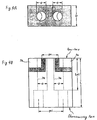
- FIG. 2A is a front view showing the open-face side of the above dielectric filter
- FIG. 2B is a bottom plan view.
- a step is provided with respect to the center axis at the depth from the open-face of L 0 , so that the resonator pitch (distance between the center axes of the inner conductor formed holes) on the open-face side is p 0 , and the resonator pitch on the short-circuiting-face side is ps.
- the inner diameters of the inner conductor formed holes 2a and 2b are constant over the range from the open-face to the short-circuiting- face, and is represented by d.
- FIG. 3 illustrates the results the Q 0 of a resonator which is changed with the ratio of the width d (inner diameter) of an inner conductor formed hole formed coaxially in a dielectric block to the width D in the longitudinal and transverse directions of the dielectric block, and is determined by the finite element method.
- the Q 0 have a large value.
- the Q 0 becomes maximum.
- the input-output electrodes 5a and 5b are capacitance-coupled with the areas near to the open-ends of the inner conductors 3a and 3b on the inner wall of the inner conductor formed holes 2a and 2b.
- the coupling coefficient between resonators is determined by the position (L - Lo where Lo and L represent line lengths on the open-face side and on the short-circuiting-face side, respectively) of steps each provided on the center axes of the inner conductor formed holes, a resonator pitch po on the open-face side, and a resonator pitch ps1 on the short-circuiting-face side.
- Lo and L represent line lengths on the open-face side and on the short-circuiting-face side, respectively
- the coupling is more capacitive, and the coupling coefficient is increased.
- the resonator pitch ps2 on the short-circuiting-face side is set to be shorter than the resonator pitch po on the open-face side, and the Lo2 is shallower, the coupling is more inductive, and as a whole, the resonators are inductive-coupled.
- the capacitive coupling is more intensified as compared with the inductive coupling by setting the resonator pitch po on the open-face side to be shorter than the resonator pitch ps1 on the short-circuiting-face side.
- the coupling of the filter shown in FIG. 6B has a further improved Q 0 . though the coupling coefficient is equal to that of the filter shown in FIG. 6A. That is, in the coupling of the filter shown in FIG.
- the line length Ls2 on the short-circuiting-face side is set to be longer than the line length Lo2 on the open-face side, correspondingly, the resonator pitch ps2 on the short-circuiting-face side is set to be longer than the ps1 of FIG. 6A, and moreover, and the resonator pitch ps2 on the short-circuiting-face side is set to be about two times the interval (D/2) between the center axis of each inner conductor formed hole and the outer conductor.
- FIGS. 7A and 7B illustrate an example of inductive-coupling the resonators.
- the inductive coupling is more intensified as compared with the capacitive coupling by setting the resonator pitch ps on the short-circuiting-face side to be shorter than the resonator pitch po1 on the open-face side.
- the coupling of the filter shown in FIG. 7B has a further improved Q 0 . though the coupling coefficient is equal to that of the filter shown in FIG. 7A. That is, in the coupling of the filter shown in FIG.
- the line length Lo2 on the open-face side is set to be longer than the line length Ls2 on the shod-circuiting-face side, correspondingly, the resonator pitch po2 on the open-face side is set to be longer than the ps1 of FIG. 7A, and moreover, and the resonator pitch po2 on the open-face side is set to be about two times the interval (D/2) between the center axis of each inner conductor formed hole and the outer conductor.
- a step is provided only at one position of the center axis of each inner conductor formed hole.
- the center axis may be shifted at two positions thereof.
- the resonator pitch in the range from the open-face to the depth Lo is po
- the resonator pitch in the range from the short-circuiting-face to the depth Ls is ps.
- the resonator pitch in the intermediate range between the above-mentioned ranges is set to have nearly a middle value between the po and the ps.
- the inner diameter of the inner conductor formed holes is constant, and is represented by d.
- one end-face of a dielectric is an open-face.
- the open-end of a resonator may be provided inside of the inner conductor formed hole or in the vicinity of the opening-portion thereof. That is, in an example shown in FIGS. 9A and 9B, an outer conductor 4 is formed on all of the six outer-faces of the dielectric block.
- Inner conductors 3a and 3b are formed on the inner walls of inner conductor formed holes 2a and 2b.
- Parts g are formed on the inner walls by partially excluding the inner conductors 3a and 3b, respectively. In this structure, the parts g are open-ends of the resonators.
- a stray capacitance is generated between the open-end of each inner conductor and the outer conductor, in the part g.
- the inner diameter d of the inner conductor formed holes 2a and 2b is set in such a manner that the Qo becomes maximum.
- steps are provided at predetermined positions of the center axes of the inner conductor formed holes 2a and 2c, respectively.
- the resonator pitch on the open-face side is set to be shorter than the resonator pitch ps on the short-circuiting-face side. Therefore, a dielectric filter in which three-stage resonators are capacitive-coupled with each other, having a band-pass characteristic is provided.
- FIG. 11A is a front view showing the open-face side of the above-described dielectric filter
- FIG. 11B is a bottom view thereof.
- the inner conductor formed holes 2a and 2b each have a square cross-section.
- a step is provided for the center axis
- the resonator pitch on the open-face side is po
- the resonator pitch on the short-circuiting-face side is ps.
- the widths of the inner conductor formed holes 2a and 2b are constant in the range from the open-face to the short-circuiting-face, respectively.
- an inner conductor formed hole has a circular cross section. As shown in FIGS. 11A and 11B, the hole may have a square cross section.
- FIG. 12 an example in which an inner conductor formed hole having a square cross section is formed in a dielectric block is discussed.
- the Qo of the resonator, changing with the ratio of d/D where D represents the width in the longitudinal, transverse directions of the dielectric block, and d represents The width of the inner conductor formed hole was determined by the finite element method. Similarly to the case shown in FIG. 3, the Qo has a large value in the range of the d/D of 0.2 - 0.4. Accordingly, the high Qo is secured by setting the width D of the dielectric block shown in FIG. 1 and the width d of the inner conductor formed holes 2a and 2b so as to have a relation of d/D 0.2 - 0.4.
- cross section of the above-described inner conductor formed holes may have the 'square cross-section' of which the corners are more or less rounded in order to prevent the ceramic from being cracked at firing.
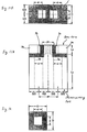
- FIG. 13A is a front view showing the dielectric duplexer viewed from the open- face side
- FIG. 13B is a bottom view thereof
- FIG. 13C is a rear elevation thereof. The rear elevation is drawn with the bottom face being positioned upward, viewed in the figure.
- six inner conductor formed holes 2a - 2f are formed in the range from one end-face of a parallelepiped-shaped dielectric block 1 to the other, opposite end-face.
- Inner conductors 3a - 3f are provided on the inner walls of these inner conductor formed holes, respectively.
- an outer conductor 4 On the outer surface of the dielectric block 1, an outer conductor 4, and moreover, input-output terminals 5a, 5b, and 5c are formed.
- the inner conductor 3c on the inner wall of the inner conductor formed hole 2c one end thereof is connected to the outer conductor 4 on the outer surface of the dielectric block, and the other end is connected to the input-output terminal 5c.
- steps are provided for the center axes of their inner conductor formed holes so that the resonator pitch on the shortcircuittting-face side and the resonators is shortened, and thereby, the resonators are capacitive-coupled with each other.
- the resonator formed of the inner conductor 3b is interdigitally-coupled with the inner conductor 3c.
- the resonator formed of the inner conductor 3d is interdigitally-coupled with the inner conductor 3c.
- the dielectric duplexer acts as such in which for example, the two-stage resonator comprising the inner conductors 3a and 3b is a transmission filter, and a band-pass filter comprising the three-stage resonator formed of the inner conductors 3d, 3e, and 3f is a reception filter.
- the input-output terminals 5a, 5b, and 5c are a transmission signal input port, a reception signal output port, and an antenna port, respectively.
- ANT represents a reception-transmission antenna, DPX a duplexer, BPFa, BPFb, and BPFd band-pass filters, respectively, AMPa and AMPb amplification circuits, respectively, MIXa and MIXb mixers, respectively, OSC an oscillator, and DIV a frequency divider (synthesizer).
- the MIXa modulates with a modulation signal a frequency signal output from the DIV.
- the BPFa passes only the transmission frequency band of the signal, which is power-amplified by the AMPa, and transmitted from the ANT through the DPX.
- the BPFb passes only the reception frequency band of a signal output from the DPX, which is amplified by the AMPb.
- the MIXb mixes a frequency signal output from the BPFc with the reception signal to output an intermediate frequency signal IF.
- the duplexer having the structure shown in FIG. 13 may be employed.
- the dielectric filter having the structure shown in FIGS. 1 to 11B may be employed.
- a communication apparatus with a low loss, making use of the high Qo filter characteristic can be formed without the size being enlarged as a whole.
Landscapes
- Engineering & Computer Science (AREA)
- General Engineering & Computer Science (AREA)
- Ocean & Marine Engineering (AREA)
- Environmental & Geological Engineering (AREA)
- Mechanical Engineering (AREA)
- Civil Engineering (AREA)
- Structural Engineering (AREA)
- Physics & Mathematics (AREA)
- Electromagnetism (AREA)
- Control Of Motors That Do Not Use Commutators (AREA)
Abstract
Description
Claims (7)
- A dielectric filter, comprising:a dielectric block (1);a plurality of inner conductor formed holes (2a, 2b; 2a ― c; 2a ― f) provided in the dielectric block (1);inner conductors (3a, 3b; 3a ― c; 3a ― f) provided on the inner walls of the inner conductor formed holes (2a, 2b; 2a ― c; 2a ― f); andouter conductor (4) provided on the outer surface of the dielectric block (1) so as to have one opening-face as an open-face of the inner conductor formed holes (2a, 2b; 2a ― c; 2a ― f), and have the other opening-face thereof as a short-circuiting-face;
wherein the sectional shape of the inner conductor formed holes (2a, 2b; 2a ― c; 2a ― f) are substantially constant in the range from the open-face to the short-circuiting-face, and a step is provided in the intermediate portion of the center axis of at least one inner conductor formed hole (2a, 2b; 2a ― c; 2a ― f). - A dielectric filter, comprising:a dielectric block (1);a plurality of inner conductor formed holes (2a, 2b; 2a ― c; 2a ― f) provided in the dielectric block (1);inner conductors (3a, 3b; 3a ― c; 3a ― f) provided on the inner walls of the inner conductor formed holes (2a, 2b; 2a ― c; 2a ― f) so as to have open-ends on the inner walls of the holes (2a, 2b; 2a ― c; 2a ― f); andouter conductor (4) provided on the outer surface of the dielectric block (1);
wherein the sectional shape of the inner conductor formed holes (2a, 2b; 2a ― c; 2a ― f) are substantially constant in the range from one opening-face of the holes (2a, 2b; 2a ― c; 2a ― f) to the other opening-face, respectively, and a step is provided in the intermediate portion of the center axis of at least one inner conductor formed hole (2a, 2b; 2a ― c; 2a ― f). - The dielectric filter according to Claim 1 or 2, wherein each of the inner conductor formed holes (2a, 2b; 2a ― c; 2a ― f) has a square cross section.
- The dielectric filter according to one of Claims 1 to 3, wherein the ratio d/D is 0.2 - 0.4 where D represents the width in the short side direction of the dielectric block (1), and d represents the width of the inner conductor formed hole (2a, 2b; 2a ― c; 2a ― f).
- The dielectric filter according to one of Claims 1 to 4, wherein the position of the step is nearer to one opening-face with respect to the center in the longitudinal direction of the inner conductor formed hole (2a, 2b), and the interval (ps2) between the center axis of the inner conductor formed hole (2a, 2b) ranging from the step to the other opening-face of the inner conductor formed hole (2a, 2b) and the center axis of an inner conductor formed hole (2a, 2b) adjacent to the inner conductor formed hole (2a, 2b) is substantially two times the interval (D/2) between each center axis and the corresponding outer conductor (4).
- A dielectric duplexer (DPX) comprising the plurality of the dielectric filters of any one of Claims 1 to 5, the dielectric filters being formed in the single dielectric block (1).
- A communication apparatus including the dielectric filter of any one of Claims 1 to 5 or the dielectric duplexer (DPX) of Claim 6.
Applications Claiming Priority (4)
| Application Number | Priority Date | Filing Date | Title |
|---|---|---|---|
| JP9592899 | 1999-04-02 | ||
| JP9592899 | 1999-04-02 | ||
| JP2000034530 | 2000-02-14 | ||
| JP2000034530A JP3528738B2 (en) | 1999-04-02 | 2000-02-14 | Dielectric filter, dielectric duplexer, and communication device |
Publications (3)
| Publication Number | Publication Date |
|---|---|
| EP1041661A2 true EP1041661A2 (en) | 2000-10-04 |
| EP1041661A3 EP1041661A3 (en) | 2001-08-22 |
| EP1041661B1 EP1041661B1 (en) | 2005-04-27 |
Family
ID=26437097
Family Applications (1)
| Application Number | Title | Priority Date | Filing Date |
|---|---|---|---|
| EP00106244A Expired - Lifetime EP1041661B1 (en) | 1999-04-02 | 2000-03-22 | Dielectric filter, dielectric duplexer, and communication apparatus |
Country Status (6)
| Country | Link |
|---|---|
| US (1) | US6496088B1 (en) |
| EP (1) | EP1041661B1 (en) |
| JP (1) | JP3528738B2 (en) |
| KR (1) | KR100338589B1 (en) |
| CN (1) | CN1186849C (en) |
| DE (1) | DE60019671T2 (en) |
Families Citing this family (3)
| Publication number | Priority date | Publication date | Assignee | Title |
|---|---|---|---|---|
| JP3788368B2 (en) * | 2001-04-10 | 2006-06-21 | 株式会社村田製作所 | Dielectric duplexer and communication device |
| JP3788369B2 (en) * | 2001-04-10 | 2006-06-21 | 株式会社村田製作所 | Dielectric filter, dielectric duplexer, and communication device |
| JP3570397B2 (en) * | 2001-06-20 | 2004-09-29 | 株式会社村田製作所 | Dielectric filter, dielectric duplexer and communication device |
Family Cites Families (7)
| Publication number | Priority date | Publication date | Assignee | Title |
|---|---|---|---|---|
| JP3344428B2 (en) * | 1992-07-24 | 2002-11-11 | 株式会社村田製作所 | Dielectric resonator and dielectric resonator component |
| JP3211547B2 (en) * | 1994-01-25 | 2001-09-25 | 株式会社村田製作所 | Dielectric filter |
| JP3175602B2 (en) * | 1996-09-19 | 2001-06-11 | 株式会社村田製作所 | Dielectric filter, duplexer and multiplexer |
| JP3577921B2 (en) * | 1997-01-13 | 2004-10-20 | 株式会社村田製作所 | Dielectric filter and dielectric duplexer |
| JP3582350B2 (en) * | 1997-04-21 | 2004-10-27 | 株式会社村田製作所 | Dielectric filter, duplexer and communication device |
| ATE280441T1 (en) * | 1998-03-18 | 2004-11-15 | Epcos Ag | MICROWAVE CERAMIC FILTER WITH IMPROVED SIDE STEEPNESS |
| JP3412546B2 (en) * | 1999-02-22 | 2003-06-03 | 株式会社村田製作所 | Dielectric filter, dielectric duplexer and communication device |
-
2000
- 2000-02-14 JP JP2000034530A patent/JP3528738B2/en not_active Expired - Lifetime
- 2000-03-22 DE DE60019671T patent/DE60019671T2/en not_active Expired - Lifetime
- 2000-03-22 EP EP00106244A patent/EP1041661B1/en not_active Expired - Lifetime
- 2000-03-30 KR KR1020000016487A patent/KR100338589B1/en not_active Expired - Lifetime
- 2000-04-03 CN CNB001064320A patent/CN1186849C/en not_active Expired - Lifetime
- 2000-04-03 US US09/541,291 patent/US6496088B1/en not_active Expired - Lifetime
Also Published As
| Publication number | Publication date |
|---|---|
| JP3528738B2 (en) | 2004-05-24 |
| KR20010006929A (en) | 2001-01-26 |
| DE60019671D1 (en) | 2005-06-02 |
| CN1186849C (en) | 2005-01-26 |
| EP1041661B1 (en) | 2005-04-27 |
| CN1269617A (en) | 2000-10-11 |
| DE60019671T2 (en) | 2006-01-19 |
| JP2000349507A (en) | 2000-12-15 |
| EP1041661A3 (en) | 2001-08-22 |
| US6496088B1 (en) | 2002-12-17 |
| KR100338589B1 (en) | 2002-05-27 |
Similar Documents
| Publication | Publication Date | Title |
|---|---|---|
| US6426725B2 (en) | Antenna device and communication device | |
| US6236288B1 (en) | Dielectric filter having at least one stepped resonator hole with a recessed or protruding portion, the stepped resonator hole extending from a mounting surface | |
| EP0986124B1 (en) | Dielectric filter, composite dielectric filter, antenna duplexer, and comunication apparatus | |
| KR100549694B1 (en) | Dielectric Filters, Dielectric Duplexers & Communications Devices | |
| JP3348658B2 (en) | Dielectric filter, composite dielectric filter, antenna duplexer, and communication device | |
| EP1041661B1 (en) | Dielectric filter, dielectric duplexer, and communication apparatus | |
| US6940364B2 (en) | Dielectric filter, dielectric duplexer, and communication apparatus | |
| US6822538B2 (en) | Dielectric filter, dielectric duplexer, and communication apparatus incorporating the same | |
| KR100338592B1 (en) | Dielectric Filter, Dielectric Duplexer and Communication Apparatus | |
| US6747527B2 (en) | Dielectric duplexer and communication apparatus | |
| KR100394804B1 (en) | Dielectric filter, dielectric duplexer, communication system, and method of producing dielectric filter | |
| JP3582465B2 (en) | Dielectric filter, dielectric duplexer and communication device | |
| US6771149B2 (en) | Dielectric filter, dielectric duplexer, and communication device | |
| US20020149442A1 (en) | Dielectric filter, dielectric duplexer, and communication device | |
| US20020130738A1 (en) | Dielectric filter, dielectric duplexer, and communication apparatus using the same |
Legal Events
| Date | Code | Title | Description |
|---|---|---|---|
| PUAI | Public reference made under article 153(3) epc to a published international application that has entered the european phase |
Free format text: ORIGINAL CODE: 0009012 |
|
| 17P | Request for examination filed |
Effective date: 20000322 |
|
| AK | Designated contracting states |
Kind code of ref document: A2 Designated state(s): AT BE CH CY DE DK ES FI FR GB GR IE IT LI LU MC NL PT SE |
|
| AX | Request for extension of the european patent |
Free format text: AL;LT;LV;MK;RO;SI |
|
| PUAL | Search report despatched |
Free format text: ORIGINAL CODE: 0009013 |
|
| AK | Designated contracting states |
Kind code of ref document: A3 Designated state(s): AT BE CH CY DE DK ES FI FR GB GR IE IT LI LU MC NL PT SE |
|
| AX | Request for extension of the european patent |
Free format text: AL;LT;LV;MK;RO;SI |
|
| RIC1 | Information provided on ipc code assigned before grant |
Free format text: 7H 01P 1/205 A, 7H 01P 1/213 B |
|
| AKX | Designation fees paid |
Free format text: DE FR GB |
|
| 17Q | First examination report despatched |
Effective date: 20030217 |
|
| GRAP | Despatch of communication of intention to grant a patent |
Free format text: ORIGINAL CODE: EPIDOSNIGR1 |
|
| GRAS | Grant fee paid |
Free format text: ORIGINAL CODE: EPIDOSNIGR3 |
|
| GRAA | (expected) grant |
Free format text: ORIGINAL CODE: 0009210 |
|
| AK | Designated contracting states |
Kind code of ref document: B1 Designated state(s): DE FR GB |
|
| REG | Reference to a national code |
Ref country code: GB Ref legal event code: FG4D |
|
| REF | Corresponds to: |
Ref document number: 60019671 Country of ref document: DE Date of ref document: 20050602 Kind code of ref document: P |
|
| PLBE | No opposition filed within time limit |
Free format text: ORIGINAL CODE: 0009261 |
|
| STAA | Information on the status of an ep patent application or granted ep patent |
Free format text: STATUS: NO OPPOSITION FILED WITHIN TIME LIMIT |
|
| ET | Fr: translation filed | ||
| 26N | No opposition filed |
Effective date: 20060130 |
|
| REG | Reference to a national code |
Ref country code: FR Ref legal event code: PLFP Year of fee payment: 17 |
|
| REG | Reference to a national code |
Ref country code: FR Ref legal event code: PLFP Year of fee payment: 18 |
|
| REG | Reference to a national code |
Ref country code: FR Ref legal event code: PLFP Year of fee payment: 19 |
|
| PGFP | Annual fee paid to national office [announced via postgrant information from national office to epo] |
Ref country code: GB Payment date: 20190320 Year of fee payment: 20 Ref country code: FR Payment date: 20190322 Year of fee payment: 20 Ref country code: DE Payment date: 20190321 Year of fee payment: 20 |
|
| REG | Reference to a national code |
Ref country code: DE Ref legal event code: R071 Ref document number: 60019671 Country of ref document: DE |
|
| REG | Reference to a national code |
Ref country code: GB Ref legal event code: PE20 Expiry date: 20200321 |
|
| PG25 | Lapsed in a contracting state [announced via postgrant information from national office to epo] |
Ref country code: GB Free format text: LAPSE BECAUSE OF EXPIRATION OF PROTECTION Effective date: 20200321 |