EP1041598A2 - Gas-discharge display apparatus - Google Patents
Gas-discharge display apparatus Download PDFInfo
- Publication number
- EP1041598A2 EP1041598A2 EP00300025A EP00300025A EP1041598A2 EP 1041598 A2 EP1041598 A2 EP 1041598A2 EP 00300025 A EP00300025 A EP 00300025A EP 00300025 A EP00300025 A EP 00300025A EP 1041598 A2 EP1041598 A2 EP 1041598A2
- Authority
- EP
- European Patent Office
- Prior art keywords
- wavelength
- optical filter
- transmittance
- nanometers
- light
- Prior art date
- Legal status (The legal status is an assumption and is not a legal conclusion. Google has not performed a legal analysis and makes no representation as to the accuracy of the status listed.)
- Granted
Links
Images






Classifications
-
- H—ELECTRICITY
- H01—ELECTRIC ELEMENTS
- H01S—DEVICES USING THE PROCESS OF LIGHT AMPLIFICATION BY STIMULATED EMISSION OF RADIATION [LASER] TO AMPLIFY OR GENERATE LIGHT; DEVICES USING STIMULATED EMISSION OF ELECTROMAGNETIC RADIATION IN WAVE RANGES OTHER THAN OPTICAL
- H01S3/00—Lasers, i.e. devices using stimulated emission of electromagnetic radiation in the infrared, visible or ultraviolet wave range
- H01S3/02—Constructional details
- H01S3/03—Constructional details of gas laser discharge tubes
-
- H—ELECTRICITY
- H01—ELECTRIC ELEMENTS
- H01J—ELECTRIC DISCHARGE TUBES OR DISCHARGE LAMPS
- H01J5/00—Details relating to vessels or to leading-in conductors common to two or more basic types of discharge tubes or lamps
- H01J5/02—Vessels; Containers; Shields associated therewith; Vacuum locks
- H01J5/16—Optical or photographic arrangements structurally combined with the vessel
Definitions
- the present invention relates to a gas-discharge display apparatus that can display color images.
- a plasma display panel that is a typical display device having a screen emitting light by gas discharge is becoming widely available as a wide screen display for a television set after the color display thereof has been succeeded in commercialization.
- PDP plasma display panel
- One of the challenges to improve the image quality of PDPs is to enhance the reproducible color range.
- an AC type PDP having three-electrode surface discharging structure is commercialized.
- This type has a pair of main electrodes for sustaining, which are arranged in parallel for each line (row) of the matrix display, and an address electrode for each column. Division walls for preventing interruption of discharge between cells are provided in stripes.
- a surface discharging structure includes a substrate on which the pairs of main electrodes are arranged and an opposing substrate on which a fluorescent layer for color display is arranged, so that deterioration of a fluorescent layer due to an ion impact upon discharge can be reduced to obtain a longer life.
- the "reflection type” that has the fluorescent layer on the back substrate is superior to the "transparent type” that has the fluorescent layer on the front substrate concerning light emission efficiency.
- Penning gas containing neon (Ne) and a trace of xenon (Xe) (4-5%) is used as a discharging gas.
- the discharging gas radiates ultraviolet rays, which excite the fluorescent material to emit light.
- Each pixel includes three cells for red (R), green (G) and blue (B) light colors, and the display color is decided by controlling the light intensity of the fluorescent material of each color.
- the composition of the fluorescent materials and the ratio of light intensities of three colors are selected so that the display color becomes white when each of the red, green and blue color light intensities is set to the maximum within the variable range.
- the fluorescent material emits light by gas discharge in a PDP
- the mixing of the light color of the discharge gas into the light color of the fluorescent material cannot be avoided. This causes a problem of deterioration of the color reproducibility.
- Fig. 13 shows a light emission spectrum of a two-component gas containing neon and xenon.
- Fig. 14 is a chromaticity diagram showing influences of the neon light emission on color reproduction.
- a plurality of light emission spectrums appears in the visible light wavelength range above 580 nanometers.
- the peak of the light emission of the discharge gas (585 nanometers) is adjacent to the maximum light emission peak (590 nanometers) of the red fluorescent material. Therefore, orange color due to the light emission of the discharge gas is added regardless of the color reproduced by the fluorescent material, so the reddish display occurs over the entire screen.
- the inside of the triangle of the solid line connecting the color coordinates of each fluorescent materials plotted with small rectangles is the reproducible color range when the color of the gas light emission is not added.
- the inside of the triangle of the broken line is the color reproducible range of the PDP measured in a darkroom.
- the real color reproducible range is narrowed compared with the original color reproducible range. Especially, reproducibility of blue and green colors is of inferior. Concerning the red color, the reproducibility is not so deteriorated since the wavelength of the gas light emission is approximate to that of the light emission of the fluorescent material.
- the red fluorescent material is different from the ideal red (620 nanometers) defined in the NTSC system. Namely, even if the influence of the gas light emission is little, it is still necessary to improve the color purity of red color.
- the display color of white pixels Since the display capacity of blue color is degraded by the gas light emission, the display color of white pixels has a low color temperature compared with the color reproduced by the fluorescent materials of three colors. It is difficult to optimize the relative light intensities of red, green and blue colors in consideration of relative luminosity factor by combining materials because there are few kinds of fluorescent materials that satisfy the use condition at present. Therefore, the color temperature of the white color is low compared with a CRT even if the color of the gas light emission is not added. Furthermore, if the color of the gas light emission is added, the color temperature drops further.
- the color temperature of the white color display is 5,000-6,000 K under the condition of the same amplitude signal applied for red, green and blue colors, while the color temperature of a CRT for a TV set in Japan is above 10,000 K. Therefore, it is necessary to raise the color temperature of the white color.
- the color temperature has different optimal values depending on the use of the display, the region (the country) where the display is used or other factor, it is preferable that the color temperature can be selected easily within the range of about 6,000-12,000 K.
- the color temperature can be raised by weakening the relative light intensities of green and red colors to blue color.
- the conventional method for adjusting the color temperature and disadvantages thereof are explained below.
- the object of the present invention is to reduce the influence of the light emission of the discharge gas for enlarging the color reproducible range, and to cause the color purity of red color to approach the ideal value. Another object of the present invention is to prevent reduction of the color temperature of white color. Still another object of the present invention is to raise the contrast without reducing the display brightness.
- an optical filter having a size uniformly covering the entire screen is arranged in an appropriate position.
- the optical filter has characteristics of selectively absorbing visible light having a wavelength within the overlapped range of the light emission wavelength range of neon or helium and the light emission wavelength range of red fluorescent material. Light within the wavelength range that can deteriorate the color reproducibility in the light emitted inside is selectively absorbed. Since the optical filter makes the proper color reproducibility, each of the fluorescent materials having different light colors can emit light with the maximum intensity in white color, for example.
- the placement of the optical filter covering the entire screen is much easier than providing a color filter for each light color of the fluorescent material.
- a gas-discharge display apparatus which utilizes at least one of neon and helium gases to generate gas discharge for exciting three kinds of fluorescent materials having different light colors to emit light for displaying a color image.
- the apparatus includes an optical filter that is an element overlapping the entire screen, being disposed in front of gas discharge space for selectively absorbing light having wavelength equal to that of light emission of the gas.
- the optical filter has characteristics in which the transmittance T 585 at the wavelength of 585 nanometers is smaller than the transmittance T 450 at the wavelength of 450 nanometers and the transmittance T 620 at the wavelength of 620 nanometers.
- the optical filter has characteristics in which the wavelength of peak absorbency in the visible light wavelength range has a value within the range of 550 to 620 nanometers.
- the apparatus includes an optical filter that is an element overlapping the entire screen, being disposed in front of gas discharge space for selectively absorbing light having wavelength equal to that of light emission of the gas.
- the optical filter has characteristics in which first and second peak absorbencies exist in the visible light wavelength range.
- the wavelength of the first peak absorbency has a value within the range of 550 to 620 nanometers
- the wavelength of the second peak absorbency has a value within the range of 500 to 550 nanometers.
- the optical filter has characteristics in which first and second peak absorbencies exist in the visible light wavelength range, the transmittance T 585 at the wavelength of 585 nanometers is smaller than the transmittance T 450 at the wavelength of 450 nanometers and the transmittance T 620 at the wavelength of 620 nanometers, and the transmittance T 525 at the wavelength of 525 nanometers is smaller than the transmittance T 450 .
- the transmittance T 585 is smaller than 0.7 times the transmittance T 450 .
- the transmittance T 585 is smaller than 0.7 times the transmittance T 450 and is smaller than the transmittance T 525 .
- the apparatus includes an optical filter that is an element overlapping the entire screen, being disposed in front of gas discharge space for selectively absorbing light having wavelength equal to that of light emission of the gas.
- the optical filter has characteristics in which first and second peak absorbencies exist in the visible light wavelength range.
- the wavelength of the first peak absorbency has a value within the range of 580 to 600 nanometers.
- the wavelength of the second peak absorbency has a value within the range of 500 to 550 nanometers.
- the transmittance of the optical filter at the first peak absorbency is smaller than 0.5 times the average transmittance in the blue wavelength range.
- the average transmittance in the green wavelength range is larger than the transmittance at the first peak absorbency and is smaller than the average transmittance in the blue wavelength range.
- the optical filter is made as a component separate from a display device having the gas discharge space, and is disposed in front of the display device.
- the optical filter is made of a film having said characteristics.
- the optical filter is in contact with the front surface of a transparent substrate making up the screen.
- the optical filter is made of an organic resin in which a substance absorbing light of a specific wavelength is dispersed.
- a non-glare layer is disposed in front of the optical filter.
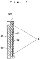
- Fig. 1 shows a structure of a plasma display apparatus 100 according to the present invention.
- the plasma display apparatus 100 includes a PDP 1 that is a color display device, a driving unit 80 for lighting cells of the PDP 1 in accordance with display contents, an optical filter 60 having spectrum transparent characteristic unique to the present invention, a front plate 92 for protecting the PDP 1, and an armor cover 90.
- the front plate 92 is made up by providing an electromagnetic shield film and an infrared cutting filter onto a substrate that is optically transparent, and applying a surface treatment for non-glare finish. Glass, acrylic resin, polycarbonate, or other materials can be used for making the substrate.
- the optical filter 60 has a dimension covering the entire screen that is a set of cells in the PDP 1, and is in intimate contact with the front surface of the PDP 1.
- the optical filter 60 can be formed by a process such as sticking a laminated filter film, sticking a film in which a pigment or a colorant is dispersed, or laminating a multicoated interference film utilizing thin film technology. Such sticking or laminating can be processed to the front surface of the PDP 1 directly, or to the front plate 92 so as to overlay on the PDP 1. Characteristics of the optical filter 60 and the front plate 92 are uniform over the entire screen.
- Figs. 2A and 2B show structures of other plasma display apparatuses, that is a variation of arrangement of the optical filter.
- the optical filter 60 contacts the back surface of the front plate 92 intimately, and is separated from the PDP 1.
- This configuration has an advantage in that the front plate 92 absorbs an external shock, so that the PDP 1 cannot be broken down easily.
- heat sink effect can be expected, i.e., the gap between the PDP 1 and the front plate 92 with the optical filter can be used as an air duct, in which external air or cooling air forced by a cooling fan can flow so as to prevent the PDP from being heated.
- the optical filter 60 contacts the PDP 1 intimately, and the front plate 92 is separated from the optical filter 60 so as to enhance protection effect.
- the optical filter 60 is formed by sticking a film, and a non-glare finish is performed before the sticking, so as to reduce an optical interface by which external light is reflected.
- the non-glare finish is preferably AG process that makes an image soft and inconspicuous by light diffusion. If AR process is used, regular reflection ratio can be reduced substantially, but an external image can be reflected clearly.
- the optical filter 60 is disposed between the PDP 1 and the front plate 92. However, the optical filter 60 can be disposed in front of the front plate 92. If the optical filter 60 is disposed in front of the light emitting portion of the PDP 1, the optical filter 60 can be formed inside the PDP 1.
- Fig. 3 is an exploded view of the PDP according to the present invention.
- the PDP 1 has first and second main electrodes X and Y making a pair arranged in parallel for generating a sustaining discharge.
- the main electrodes X, Y and an address electrode A as a third electrode cross to make a three-electrode surface discharge structure.
- the main electrodes X and Y extend in the row direction of the screen (the horizontal direction), and the second main electrode Y is used as a scan electrode for selecting cells in a row upon addressing.
- the address electrode A extends in the column direction (the vertical direction), and is used as a data electrode for selecting cells in a column.
- the area of the substrate where the main electrodes and the address electrodes cross is the display screen.
- a pair of main electrodes X and Y is arranged in each row on the inner surface of a glass substrate 11 that is a substrate of a front substrate structure 10.
- the row is a line of cells in the horizontal direction of the screen.
- Each of the main electrodes X and Y includes a transparent conductive film 41 and a metal film (a bus conductor) 42, and is covered with an insulating layer 17 having a thickness of approximately 30 microns made of low-melting glass.
- the surface of the insulating layer 17 is coated with a protection film 18 made of magnesia (MgO) having a thickness of several thousands angstroms.
- MgO magnesia
- the address electrodes A are arranged on the inner surface of a glass substrate 21 that is a substrate of a rear substrate structure 20, and is covered with an insulating layer 24 having a thickness of approximately 10 microns.
- an insulating layer 24 having a thickness of approximately 10 microns.
- a division wall 29 having a shape like a band of height 150 microns viewed from the top is disposed at each space between the neighboring address electrodes. These division walls 29 divide the discharging space 30 in the row direction into plural subpixel (plural unit lighting regions), and define the gap size of the discharging space 30.
- red fluorescent material 28R, green fluorescent material 28G and blue fluorescent material 28B for color display are arranged coating the inner surface of the rear side including the upper portion of the address electrode A and the side surface of the division wall 29, so that the three colors are arranged in a periodic pattern.
- the fluorescent materials 28R, 28G and 28B are selected so that white color is reproduced when each of them emits light in the maximum intensity, and the forming shapes of them are the same.
- a preferred example of the fluorescent materials is shown in TABLE 1.
- the discharging space 30 is filled with a discharging gas containing neon as a base and xenon (4-5%), and each color of the fluorescent materials 28R, 28G and 28B is partially exited by ultraviolet rays emitted by xenon upon discharging so as to emit light.
- a color balance of red, green and blue colors can be adjusted by designing the characteristics of the optical filter 60. Therefore, it is not required to select the fluorescent materials severely or to adjust the forming shape of the fluorescent material of each color for optimizing the color balance.
- One element of display (a pixel) includes three subpixels having different light colors arranged in the row direction.
- the structure of each subpixel is the cell. Since the division walls 29 are arranged in a stripe pattern, the portion of the discharging space 30 corresponding to each column is continuous over all rows.
- An electrode gap between neighboring rows is set to a value substantially larger than the surface discharge gap (e.g., 80-140 microns), which can prevent discharge connection in the column direction, e.g. a value within a range of 400-500 microns.
- the address discharge is generated between the main electrode Y and the address electrode A of a cell to be lightened (in the case of write address format) or a cell to be not lightened (in the case of erase address format), so that a charged state is formed in each row where only the cells to be lightened have an appropriate quantity of wall discharge. Then, a sustaining voltage Vs is applied between the main electrodes X and Y, so that the cells to be lightened can generate surface discharge.
- Ne-Xe (4%) Penning gas is used as the discharging gas, which emits light having the spectrum shown in Fig. 13.
- any gas containing helium (He) or krypton (Kr) can be used as the discharging gas regardless of whether neon is contained or not.
- Helium and krypton emit light having a wavelength in the range of 580 ⁇ 600 nanometers in the same way as neon, so the optical filter 60 of the present invention having wavelength selecting property is effective.
- Figs. 4A and 4B show the light emission spectrums of blue and red displays.
- the light emission spectrum in which only the blue fluorescent material 28B is exited to emit light, includes a light emission spectrum of the fluorescent material in the wavelength range of 400-550 nanometers, as well as a light emission spectrum of neon in the wavelength range above 580 nanometers. If this light emission above 580 nanometers can be eliminated by the filter, purity of blue color will be improved.
- the light emission spectrum of the red fluorescent material 28R has substantially three peaks at wavelengths of 595 nanometers, 610 nanometers and 625 nanometers, and the distribution range is substantially overlapped with that of the light emission spectrum of neon.
- the filter that eliminates entire light emission spectrum of neon also eliminates the light emission of red color, and causes substantial deterioration of intensity of red display.
- the inventors have studied about the wavelength range to be eliminated, and obtained the following result. Namely, if the wavelength spectrum of the light emission spectrum in which the product of the light intensity and the relative luminosity factor becomes the maximum, i.e., 585 nanometers and surrounding wavelength spectrum is eliminated, the purities of blue and green colors can be improved with suppressing the deterioration of red color intensity at the minimum. In addition, the spectrum of red light emission approaches the monochrome light emission of 620 nanometers that is the ideal in NTSC standard.
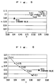
- Fig. 5 is a chromaticity diagram showing the result of the filter having a peak absorbency wavelength of 590 nanometers in blue color display.
- Fig. 6 is a chromaticity diagram showing the result of the filter having a peak absorbency wavelength of 590 nanometers in red color display.
- an imaginary filter having an ideal absorbency characteristics as shown in Fig. 7 is supposed for studying about the relationship between the transmittance T and the chromaticity at the peak absorbency.
- the chromaticity of blue color is improved and approaches the ideal value (NTSC standard) when the transmittance at the peak absorbency decreases.
- the chromaticity approaches the ideal value along with the transmittance being decreased.
- the improvement of the color temperature will be explained next.
- the light intensity of red color decreases and the coordinate of the white color on the chromaticity diagram moves in the direction in which the x value decreases.
- the color temperature increases as the arrow in Fig. 8 shows.
- the chromaticity coordinate in white color be on the blackbody radiation curve shown by the thick line in the figure.
- the light intensity of only red color is attenuated, deviation from the blackbody radiation in the Y-axis direction increases along with the increase of the attenuation.
- white color becomes greeny white.
- the filter preferably has a characteristic having peak absorbency in the green color wavelength range, too.
- the transmittance of the filter is set so that the light intensity of the green color decreases to the extent corresponding to the decrease of red color, so that the chromaticity coordinate of the white color can be corrected to be a coordinate on the blackbody radiation curve.
- Such adjustment of color temperature though it causes decrease of light intensity due to transparency of the filter, has advantages in that the bright-room contrast is improved in contrast to the adjustment of the signal amplitude that is adopted in the conventional technique, and in that the optimal color temperature can be realized easily in accordance with the use only by changing the filter characteristic.
- the reason why the bright-room contrast is improved is as follows.
- the improvement of the color purity and the adjustment of the color temperature according to the present invention do not reduce the light intensity L 0 since the adjustment of fluorescent material, the cell structure, and the signal amplitude.
- the improvement of the color purity and the adjustment of the color temperature are achieved by reducing the transmittance T, so that the bright-room contrast is improved.
- Fig. 9 shows a first example of the characteristics of the optical filter 60.
- the transparency is shown by a thick solid line and the light emission spectrum of the fluorescent material is shown by a thin solid line for a reference.
- the peak absorbency wavelength in the visible light wavelength range is 590 nanometers, a value within the range of 550-620 nanometers.
- the transmittance T 585 at the wavelength of 585 nanometers is smaller than both the transmittance T 450 at the wavelength of 450 nanometers and the transmittance T 620 at the wavelength of 620 nanometers.
- Such characteristics are obtained by forming a pigment layer that can absorb light of the wavelength 585 nanometers on a polyethylene film having thickness of 200 microns.
- a pigment layer that can absorb light of the wavelength 585 nanometers on a polyethylene film having thickness of 200 microns.
- the pigment 1-Ethyl-4-[(1-ethyl-4(1H)-quinolinylidene) methyl]quinolinium iodide whose peak absorbency (Absorption Maximum) is 590 nanometers (KABUSIKIGAISHA NIPPON KANKOUSHIKISO KENKYUUSHO Product Number NK-6), and 3-Ethyl-2-[3-(1-ethyl-4(1H)-quinolinylidene)-1-propenyl]benzoxazoli um iodide whose peak absorbency is 594 nanometers (KABUSIKIGAISHA NIPPON KANKOUSHIKISO KENKYUUSHO Product Number
- the peak absorbency wavelength of the filter is identical to the gas light emission wavelength, some beneficial result can be obtained if the peak absorbency is in the range of approximately 550-620 nanometers. However, if the difference between the peak absorbency wavelength and the gas light emission wavelength is large, the absorbency wavelength range should be widened, resulting in increase of filter color. Therefore, the appropriate value of the peak absorbency wavelength is in the range of 580 ⁇ 600 nanometers.
- Fig. 10 is a chromaticity diagram showing the color reproducible range corresponding to the characteristics of Fig. 9.
- the color reproducible range connecting the chromaticity points of red, green and blue colors without the optical filter 60 is shown by the triangle in the broken line, and the chromaticity coordinate of white color is shown by the black dot.
- the color reproducible range with the optical filter 60 is shown by the triangle in the solid line, and the chromaticity coordinate of white color is shown by the x mark.
- the color reproducible range is enlarged in all ranges of red, green and blue colors, and the chromaticity coordinate of the white color is reduced both in X and Y (i.e., the color temperature is raised).
- the color temperature is raised from 5,000 K to 7,000 K.
- the chromaticity coordinate of white color is a little shifted upward from the blackbody radiation curve shown in the solid line to be greeny white color.
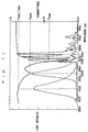
- Fig. 11 shows a second example of the characteristics of the optical filter 60.
- the transparency is shown by a thick solid line and the light emission spectrum of the fluorescent material is shown by a thin solid line for a reference.
- an absorbency is added whose peak wavelength is close to the wavelength of 525 nanometers that is a light emission peak wavelength of the green color fluorescent material 28G so as to solve the problem of the color temperature in the characteristics of Fig. 9.
- a first peak absorbency wavelength is a value within the range of 550-620 nanometers (585 nanometers)
- a second peak absorbency wavelength is a value within the range of 500-550 nanometers (525 nanometers).
- the transmittance T 585 at the wavelength of 585 nanometers is smaller than both the transmittance T 450 at the wavelength of 450 nanometers and the transmittance T 620 at the wavelength of 620 nanometers.
- the transmittance T 525 at the wavelength of 525 nanometers is smaller than the transmittance T 450 .
- the transmittance T 585 is smaller than 0.7 times the transmittance T 450 and is smaller than 0.5 times the average transmittance in the blue color wavelength range (distributed light emission of blue color fluorescent material).
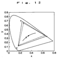
- Fig. 12 is a chromaticity diagram showing the color reproducible range corresponding to the characteristics of Fig. 11.
- the color reproducible range connecting the chromaticity points of red, green and blue colors without the optical filter 60 is shown by the triangle in the broken line, and the chromaticity coordinate of white color is shown by the black dot.
- the color reproducible range in the state with the optical filter 60 is shown by the triangle in the solid line, and the chromaticity coordinate of white color is shown by the x mark.
- the color reproducible range is enlarged in all ranges of red, green and blue colors, and the chromaticity coordinate of the white color is reduced both in X and Y (i.e., the color temperature is raised).
- the color temperature is raised from 5,000 K to 7,000 K.
- the chromaticity coordinate of white color is on the blackbody radiation curve, to be ideal coordinate.
- the bright-room contrast when the illumination of the PDP 1 at the front surface is 3001x is further improved from 20:1 to 40:1 by the arrangement of the optical filter 60 having the characteristics shown in Fig. 11.
- the color temperature can be adjusted to any value within the range of 5,000-13,000 K by controlling the spectrum transparent characteristic of the optical filter 60. More specifically, if the absorption quantity around 590 nanometers in Fig. 11 is increased so that the transmittance becomes less than 10%, a color temperature above 10,000 K can be achieved and the same performance as a CRT for TV set can be realized. If the absorption quantity around 590 nanometers is decreased to that the transmittance becomes approximately 50%, a color temperature about 6,500 K can be achieved and the same performance a CRT for publishing or designing use or a CRT for a TV set used in Europe can be realized. Namely, a display apparatus having the optimum color reproducibility for use and area (country) can be provided by changing the spectrum transparent characteristic of the optical filter 60 without changing the material and the structure of the PDP 1, so that cost reduction of the apparatus can be realized.
Landscapes
- Physics & Mathematics (AREA)
- Electromagnetism (AREA)
- Engineering & Computer Science (AREA)
- Plasma & Fusion (AREA)
- Optics & Photonics (AREA)
- Gas-Filled Discharge Tubes (AREA)
- Devices For Indicating Variable Information By Combining Individual Elements (AREA)
- Vessels And Coating Films For Discharge Lamps (AREA)
Abstract
Description
| PREFERRED FLUORESCENT MATERIALS | |
| Light Emission Color | Fluorescent Material |
| Red | (Y, Gd)BO3: Eu |
| Green | Zn2SiO4: Mn |
| Blue | BaMgAl19O17: Eu |
Claims (17)
- A gas-discharge display apparatus utilizing at least one of neon and helium gases to generate gas discharge for exciting three kinds of fluorescent materials having different light colors to emit light for displaying a color image, wherein the apparatus includes an optical filter that is an element overlapping the entire screen, being disposed in front of gas discharge space for selectively absorbing light having wavelength equal to that of light emission of the gas, and the optical filter has characteristics in which the transmittance T585 at the wavelength of 585 nanometers is smaller than the transmittance T450 at the wavelength of 450 nanometers and the transmittance T620 at the wavelength of 620 nanometers.
- The apparatus according to claim 1, wherein the optical filter has characteristics in which the wavelength of peak absorbency in the visible light wavelength range has a value within the range of 550 to 620 nanometers.
- A gas-discharge display apparatus utilizing at least one of neon and helium gases to generate gas discharge for exciting three kinds of fluorescent materials having different light colors to emit light for displaying a color image, wherein the apparatus includes an optical filter that is an element overlapping the entire screen, being disposed in front of gas discharge space for selectively absorbing light having wavelength equal to that of light emission of the gas, the optical filter has characteristics in which first and second peak absorbencies exist in the visible light wavelength range, the wavelength of the first peak absorbency has a value within the range of 550 to 620 nanometers, and the wavelength of the second peak absorbency has a value within the range of 500 to 550 nanometers.
- A gas-discharge display apparatus utilizing at least one of neon and helium gases to generate gas discharge for exciting three kind of fluorescent materials having different light colors to emit light for displaying a color image, wherein the apparatus includes an optical filter that is an element overlapping the entire screen, being disposed in front of gas discharge space for selectively absorbing light having wavelength equal to that of light emission of the gas, the optical filter has characteristics in which first and second peak absorbencies exist in the visible light wavelength range, the transmittance T585 at the wavelength of 585 nanometers is smaller than the transmittance T450 at the wavelength of 450 nanometers and the transmittance T620 at the wavelength of 620 nanometers, and the transmittance T525 at the wavelength of 525 nanometers is smaller than the transmittance T450.
- The apparatus according to claim 1 or 4, wherein the transmittance T585 is smaller than 0.7 times the transmittance T450.
- The apparatus according to claim 4, wherein the transmittance T585 is smaller than 0.7 times the transmittance T450 and is smaller than the transmittance T 525.
- The apparatus according to claim 1, wherein the optical filter is made as a component separate from a display device having the gas discharge space, and is disposed in front of the display device.
- The apparatus according to claim 7, wherein the optical filter is made of a film having said characteristics.
- The apparatus according to claim 1, wherein the optical filter is in contact with the front surface of a transparent substrate making up the screen.
- The apparatus according to claim 1, wherein the optical filter is made of an organic resin in which a substance absorbing light of a specific wavelength is dispersed.
- The apparatus according to claim 1, wherein a non-glare layer is disposed in front of the optical filter.
- A gas-discharge display apparatus utilizing at least one of neon and helium gases to generate gas discharge for exciting three kinds of fluorescent materials having different light colors to emit light for displaying a color image, wherein the apparatus includes an optical filter that is an element overlapping the entire screen, being disposed in front of gas discharge space for selectively absorbing light having wavelength equal to that of light emission of the gas, the optical filter has characteristics in which first and second peak absorbencies exist in the visible light wavelength range, the wavelength of the first peak absorbency has a value within the range of 580 to 600 nanometers, the wavelength of the second peak absorbency has a value within the range of 500 to 550 nanometers, the transmittance of the optical filter at the first peak absorbency is smaller than 0.5 times the average transmittance in the blue wavelength range, and the average transmittance in the green wavelength range is larger than the transmittance at the first peak absorbency and is smaller than the average transmittance in the blue wavelength range.
- The apparatus according to claim 12, wherein the optical filter is made as a component separate from a display device having the gas discharge space, and is disposed in front of the display device.
- The apparatus according to claim 12, wherein the optical filter is made of a film having said characteristics.
- The apparatus according to claim 12, wherein the optical filter is in contact with the front surface of a transparent substrate making up the screen.
- The apparatus according to claim 12, wherein the optical filter is made of an organic resin in which a substance absorbing light of a specific wavelength is dispersed.
- The apparatus according to claim 12, wherein a non-glare layer is disposed in front of the optical filter.
Applications Claiming Priority (2)
| Application Number | Priority Date | Filing Date | Title |
|---|---|---|---|
| JP9109199 | 1999-03-31 | ||
| JP09109199A JP3576032B2 (en) | 1999-03-31 | 1999-03-31 | Gas discharge display |
Publications (3)
| Publication Number | Publication Date |
|---|---|
| EP1041598A2 true EP1041598A2 (en) | 2000-10-04 |
| EP1041598A3 EP1041598A3 (en) | 2000-11-22 |
| EP1041598B1 EP1041598B1 (en) | 2005-07-27 |
Family
ID=14016861
Family Applications (1)
| Application Number | Title | Priority Date | Filing Date |
|---|---|---|---|
| EP00300025A Expired - Lifetime EP1041598B1 (en) | 1999-03-31 | 2000-01-05 | Gas-discharge display apparatus |
Country Status (5)
| Country | Link |
|---|---|
| US (1) | US6888301B1 (en) |
| EP (1) | EP1041598B1 (en) |
| JP (1) | JP3576032B2 (en) |
| KR (1) | KR100583287B1 (en) |
| DE (1) | DE60021462T2 (en) |
Cited By (2)
| Publication number | Priority date | Publication date | Assignee | Title |
|---|---|---|---|---|
| EP1107280A1 (en) * | 1999-12-07 | 2001-06-13 | Fujitsu Limited | Gas discharge display device |
| EP1398813A3 (en) * | 2002-09-10 | 2008-07-30 | Fujitsu Hitachi Plasma Display Limited | Gas discharge display device |
Families Citing this family (11)
| Publication number | Priority date | Publication date | Assignee | Title |
|---|---|---|---|---|
| GB2373636B (en) | 2000-11-29 | 2004-09-08 | Mitsubishi Chem Corp | Semiconductor light emitting device with two heat sinks in contact with each other |
| WO2002052531A1 (en) * | 2000-12-19 | 2002-07-04 | Bridgestone Corporation | Plasma display filmand protection filter, and plasma display |
| JP2002189422A (en) * | 2000-12-19 | 2002-07-05 | Bridgestone Corp | Film and protective filter for plasma display |
| JP2002313242A (en) * | 2001-04-10 | 2002-10-25 | Pioneer Electronic Corp | Plasma display panel |
| JP2002352736A (en) * | 2001-05-28 | 2002-12-06 | Matsushita Electric Ind Co Ltd | Plasma display |
| JP2004170788A (en) * | 2002-11-21 | 2004-06-17 | Toshiba Corp | Optical filter and display device having the same |
| KR100764761B1 (en) * | 2003-02-12 | 2007-10-11 | 엘지전자 주식회사 | Front filter |
| KR100768200B1 (en) * | 2006-02-01 | 2007-10-17 | 삼성에스디아이 주식회사 | Optical filter and plasma display panel using the same |
| KR20070084940A (en) * | 2006-02-22 | 2007-08-27 | 삼성코닝 주식회사 | Display filter and display device including the same |
| WO2011028146A1 (en) * | 2009-09-04 | 2011-03-10 | Korotkov Konstantin Georgievich | Method for determining the condition of a biological object and device for making same |
| TWI454757B (en) * | 2012-08-15 | 2014-10-01 | Au Optronics Corp | Optical touch display device and color filter thereof |
Family Cites Families (18)
| Publication number | Priority date | Publication date | Assignee | Title |
|---|---|---|---|---|
| JPS5849641A (en) | 1981-09-21 | 1983-03-23 | Hoya Corp | Contrast filter for color crt display device |
| US4987338A (en) * | 1988-03-31 | 1991-01-22 | Kabushiki Kaisha Toshiba | Cathode ray tube with film on face-plate |
| US5121030A (en) * | 1989-05-03 | 1992-06-09 | Honeywell Inc. | Absorption filters for chlor display devices |
| US5218268A (en) * | 1989-10-31 | 1993-06-08 | Kabushiki Kaisha Toshiba | Optical filter for cathode ray tube |
| US5178955A (en) * | 1990-12-17 | 1993-01-12 | Allied-Signal Inc. | Polymeric anti-reflection coatings and coated articles |
| JP3121090B2 (en) * | 1992-01-24 | 2000-12-25 | 富士通株式会社 | Plasma display panel |
| EP0596531B1 (en) * | 1992-11-06 | 1997-07-09 | Kabushiki Kaisha Toshiba | Antireflection film and display apparatus comprising the same |
| JPH08123364A (en) * | 1994-10-20 | 1996-05-17 | Fujitsu General Ltd | Color correction device |
| JPH08138559A (en) * | 1994-11-11 | 1996-05-31 | Hitachi Ltd | Plasma display device |
| JPH0922657A (en) | 1995-07-03 | 1997-01-21 | Dainippon Printing Co Ltd | Plasma display panel |
| JP3145279B2 (en) * | 1995-08-28 | 2001-03-12 | 大日本印刷株式会社 | Plasma display panel and method of manufacturing the same |
| JPH0992162A (en) * | 1995-09-20 | 1997-04-04 | Hitachi Ltd | Plasma display panel |
| JP3674146B2 (en) * | 1996-05-07 | 2005-07-20 | 株式会社富士通ゼネラル | Optical filter device |
| US5834122A (en) | 1996-11-25 | 1998-11-10 | Hoechst Celanese Corp. | Spectrally tuned multiple bandpass filters for video displays |
| KR20000070211A (en) * | 1997-11-17 | 2000-11-25 | 모리 데쯔지 | Plasma display substrate glass |
| JPH11233033A (en) | 1997-11-17 | 1999-08-27 | Nippon Electric Glass Co Ltd | Substrate glass for plasma display |
| JP3410024B2 (en) | 1998-06-18 | 2003-05-26 | 富士通株式会社 | Gas discharge display |
| US6157504A (en) * | 1998-10-20 | 2000-12-05 | Fuji Photo Film Co., Ltd. | Optical filter comprising transparent support and filter layer having two absorption maximums |
-
1999
- 1999-03-31 JP JP09109199A patent/JP3576032B2/en not_active Expired - Fee Related
- 1999-11-12 KR KR1019990050126A patent/KR100583287B1/en not_active Expired - Fee Related
- 1999-12-28 US US09/473,047 patent/US6888301B1/en not_active Expired - Fee Related
-
2000
- 2000-01-05 EP EP00300025A patent/EP1041598B1/en not_active Expired - Lifetime
- 2000-01-05 DE DE60021462T patent/DE60021462T2/en not_active Expired - Lifetime
Cited By (3)
| Publication number | Priority date | Publication date | Assignee | Title |
|---|---|---|---|---|
| EP1107280A1 (en) * | 1999-12-07 | 2001-06-13 | Fujitsu Limited | Gas discharge display device |
| US6909225B1 (en) | 1999-12-07 | 2005-06-21 | Fujitsu Limited | Gas discharge display device |
| EP1398813A3 (en) * | 2002-09-10 | 2008-07-30 | Fujitsu Hitachi Plasma Display Limited | Gas discharge display device |
Also Published As
| Publication number | Publication date |
|---|---|
| US6888301B1 (en) | 2005-05-03 |
| DE60021462D1 (en) | 2005-09-01 |
| DE60021462T2 (en) | 2006-02-16 |
| JP2000284704A (en) | 2000-10-13 |
| EP1041598A3 (en) | 2000-11-22 |
| KR100583287B1 (en) | 2006-05-25 |
| JP3576032B2 (en) | 2004-10-13 |
| EP1041598B1 (en) | 2005-07-27 |
| KR20000062156A (en) | 2000-10-25 |
Similar Documents
| Publication | Publication Date | Title |
|---|---|---|
| US20070152587A1 (en) | Gas discharge display device with particular filter characteristics | |
| US6348762B1 (en) | Surface discharge type color plasma display panel | |
| US6670754B1 (en) | Gas discharge display and method for producing the same | |
| US20040263078A1 (en) | Plasma display panel | |
| EP1041598B1 (en) | Gas-discharge display apparatus | |
| EP1804270B1 (en) | Light blocking layer, display filter having the light blocking layer, and display apparatus having the display filter | |
| US20020008473A1 (en) | Plasma display panel | |
| JP3625719B2 (en) | Gas discharge display device | |
| JP2000348627A (en) | Substrate for AC plasma display panel, AC plasma display panel, and AC plasma display device | |
| KR100749615B1 (en) | Plasma display panel | |
| JP3934771B2 (en) | Gas discharge display panel | |
| US20050264233A1 (en) | Plasma display panel (PDP) | |
| KR100578980B1 (en) | Plasma display panel | |
| JP2003257326A (en) | Plasma display panel, and manufacturing method therefor | |
| KR100502921B1 (en) | Plasma display panel | |
| EP1398813A2 (en) | Gas discharge display device | |
| KR20020018894A (en) | Plasma display panel | |
| KR20080044027A (en) | Plasma display panel | |
| KR20050113899A (en) | Plasma display panel | |
| KR20080105544A (en) | Plasma display panel | |
| KR20080042331A (en) | Plasma display panel |
Legal Events
| Date | Code | Title | Description |
|---|---|---|---|
| PUAI | Public reference made under article 153(3) epc to a published international application that has entered the european phase |
Free format text: ORIGINAL CODE: 0009012 |
|
| AK | Designated contracting states |
Kind code of ref document: A2 Designated state(s): DE FR GB NL |
|
| AX | Request for extension of the european patent |
Free format text: AL;LT;LV;MK;RO;SI |
|
| PUAL | Search report despatched |
Free format text: ORIGINAL CODE: 0009013 |
|
| AK | Designated contracting states |
Kind code of ref document: A3 Designated state(s): AT BE CH CY DE DK ES FI FR GB GR IE IT LI LU MC NL PT SE |
|
| AX | Request for extension of the european patent |
Free format text: AL;LT;LV;MK;RO;SI |
|
| 17P | Request for examination filed |
Effective date: 20010228 |
|
| AKX | Designation fees paid |
Free format text: DE FR GB NL |
|
| 17Q | First examination report despatched |
Effective date: 20030918 |
|
| GRAP | Despatch of communication of intention to grant a patent |
Free format text: ORIGINAL CODE: EPIDOSNIGR1 |
|
| GRAS | Grant fee paid |
Free format text: ORIGINAL CODE: EPIDOSNIGR3 |
|
| GRAA | (expected) grant |
Free format text: ORIGINAL CODE: 0009210 |
|
| AK | Designated contracting states |
Kind code of ref document: B1 Designated state(s): DE FR GB NL |
|
| REG | Reference to a national code |
Ref country code: GB Ref legal event code: FG4D |
|
| REF | Corresponds to: |
Ref document number: 60021462 Country of ref document: DE Date of ref document: 20050901 Kind code of ref document: P |
|
| ET | Fr: translation filed | ||
| PLBE | No opposition filed within time limit |
Free format text: ORIGINAL CODE: 0009261 |
|
| STAA | Information on the status of an ep patent application or granted ep patent |
Free format text: STATUS: NO OPPOSITION FILED WITHIN TIME LIMIT |
|
| 26N | No opposition filed |
Effective date: 20060428 |
|
| PGFP | Annual fee paid to national office [announced via postgrant information from national office to epo] |
Ref country code: FR Payment date: 20130204 Year of fee payment: 14 Ref country code: GB Payment date: 20130102 Year of fee payment: 14 Ref country code: DE Payment date: 20130103 Year of fee payment: 14 |
|
| PGFP | Annual fee paid to national office [announced via postgrant information from national office to epo] |
Ref country code: NL Payment date: 20130116 Year of fee payment: 14 |
|
| REG | Reference to a national code |
Ref country code: DE Ref legal event code: R119 Ref document number: 60021462 Country of ref document: DE |
|
| REG | Reference to a national code |
Ref country code: NL Ref legal event code: V1 Effective date: 20140801 |
|
| GBPC | Gb: european patent ceased through non-payment of renewal fee |
Effective date: 20140105 |
|
| REG | Reference to a national code |
Ref country code: DE Ref legal event code: R119 Ref document number: 60021462 Country of ref document: DE Effective date: 20140801 |
|
| PG25 | Lapsed in a contracting state [announced via postgrant information from national office to epo] |
Ref country code: DE Free format text: LAPSE BECAUSE OF NON-PAYMENT OF DUE FEES Effective date: 20140801 Ref country code: NL Free format text: LAPSE BECAUSE OF NON-PAYMENT OF DUE FEES Effective date: 20140801 |
|
| REG | Reference to a national code |
Ref country code: FR Ref legal event code: ST Effective date: 20140930 |
|
| PG25 | Lapsed in a contracting state [announced via postgrant information from national office to epo] |
Ref country code: GB Free format text: LAPSE BECAUSE OF NON-PAYMENT OF DUE FEES Effective date: 20140105 Ref country code: FR Free format text: LAPSE BECAUSE OF NON-PAYMENT OF DUE FEES Effective date: 20140131 |