EP1041418A2 - Optical wiring layer, optoelectric wiring substrate, mounted substrate, and methods for manufacturing the same - Google Patents
Optical wiring layer, optoelectric wiring substrate, mounted substrate, and methods for manufacturing the same Download PDFInfo
- Publication number
- EP1041418A2 EP1041418A2 EP00106748A EP00106748A EP1041418A2 EP 1041418 A2 EP1041418 A2 EP 1041418A2 EP 00106748 A EP00106748 A EP 00106748A EP 00106748 A EP00106748 A EP 00106748A EP 1041418 A2 EP1041418 A2 EP 1041418A2
- Authority
- EP
- European Patent Office
- Prior art keywords
- substrate
- core
- wiring layer
- optical
- optical wiring
- Prior art date
- Legal status (The legal status is an assumption and is not a legal conclusion. Google has not performed a legal analysis and makes no representation as to the accuracy of the status listed.)
- Granted
Links
Images


















Classifications
-
- G—PHYSICS
- G02—OPTICS
- G02B—OPTICAL ELEMENTS, SYSTEMS OR APPARATUS
- G02B6/00—Light guides; Structural details of arrangements comprising light guides and other optical elements, e.g. couplings
- G02B6/24—Coupling light guides
- G02B6/42—Coupling light guides with opto-electronic elements
- G02B6/4201—Packages, e.g. shape, construction, internal or external details
- G02B6/4204—Packages, e.g. shape, construction, internal or external details the coupling comprising intermediate optical elements, e.g. lenses, holograms
- G02B6/4214—Packages, e.g. shape, construction, internal or external details the coupling comprising intermediate optical elements, e.g. lenses, holograms the intermediate optical element having redirecting reflective means, e.g. mirrors, prisms for deflecting the radiation from horizontal to down- or upward direction toward a device
-
- H—ELECTRICITY
- H05—ELECTRIC TECHNIQUES NOT OTHERWISE PROVIDED FOR
- H05K—PRINTED CIRCUITS; CASINGS OR CONSTRUCTIONAL DETAILS OF ELECTRIC APPARATUS; MANUFACTURE OF ASSEMBLAGES OF ELECTRICAL COMPONENTS
- H05K1/00—Printed circuits
- H05K1/18—Printed circuits structurally associated with non-printed electric components
-
- G—PHYSICS
- G02—OPTICS
- G02B—OPTICAL ELEMENTS, SYSTEMS OR APPARATUS
- G02B6/00—Light guides; Structural details of arrangements comprising light guides and other optical elements, e.g. couplings
- G02B6/10—Light guides; Structural details of arrangements comprising light guides and other optical elements, e.g. couplings of the optical waveguide type
- G02B6/12—Light guides; Structural details of arrangements comprising light guides and other optical elements, e.g. couplings of the optical waveguide type of the integrated circuit kind
- G02B6/13—Integrated optical circuits characterised by the manufacturing method
- G02B6/138—Integrated optical circuits characterised by the manufacturing method by using polymerisation
-
- G—PHYSICS
- G02—OPTICS
- G02B—OPTICAL ELEMENTS, SYSTEMS OR APPARATUS
- G02B6/00—Light guides; Structural details of arrangements comprising light guides and other optical elements, e.g. couplings
- G02B6/24—Coupling light guides
- G02B6/42—Coupling light guides with opto-electronic elements
-
- G—PHYSICS
- G02—OPTICS
- G02B—OPTICAL ELEMENTS, SYSTEMS OR APPARATUS
- G02B6/00—Light guides; Structural details of arrangements comprising light guides and other optical elements, e.g. couplings
- G02B6/24—Coupling light guides
- G02B6/42—Coupling light guides with opto-electronic elements
- G02B6/4201—Packages, e.g. shape, construction, internal or external details
-
- G—PHYSICS
- G02—OPTICS
- G02B—OPTICAL ELEMENTS, SYSTEMS OR APPARATUS
- G02B6/00—Light guides; Structural details of arrangements comprising light guides and other optical elements, e.g. couplings
- G02B6/24—Coupling light guides
- G02B6/42—Coupling light guides with opto-electronic elements
- G02B6/4201—Packages, e.g. shape, construction, internal or external details
- G02B6/4274—Electrical aspects
-
- H—ELECTRICITY
- H05—ELECTRIC TECHNIQUES NOT OTHERWISE PROVIDED FOR
- H05K—PRINTED CIRCUITS; CASINGS OR CONSTRUCTIONAL DETAILS OF ELECTRIC APPARATUS; MANUFACTURE OF ASSEMBLAGES OF ELECTRICAL COMPONENTS
- H05K1/00—Printed circuits
- H05K1/02—Details
- H05K1/0274—Optical details, e.g. printed circuits comprising integral optical means
-
- G—PHYSICS
- G02—OPTICS
- G02B—OPTICAL ELEMENTS, SYSTEMS OR APPARATUS
- G02B6/00—Light guides; Structural details of arrangements comprising light guides and other optical elements, e.g. couplings
- G02B6/24—Coupling light guides
- G02B6/42—Coupling light guides with opto-electronic elements
- G02B6/4201—Packages, e.g. shape, construction, internal or external details
- G02B6/4219—Mechanical fixtures for holding or positioning the elements relative to each other in the couplings; Alignment methods for the elements, e.g. measuring or observing methods especially used therefor
- G02B6/422—Active alignment, i.e. moving the elements in response to the detected degree of coupling or position of the elements
- G02B6/4221—Active alignment, i.e. moving the elements in response to the detected degree of coupling or position of the elements involving a visual detection of the position of the elements, e.g. by using a microscope or a camera
- G02B6/4224—Active alignment, i.e. moving the elements in response to the detected degree of coupling or position of the elements involving a visual detection of the position of the elements, e.g. by using a microscope or a camera using visual alignment markings, e.g. index methods
-
- G—PHYSICS
- G02—OPTICS
- G02B—OPTICAL ELEMENTS, SYSTEMS OR APPARATUS
- G02B6/00—Light guides; Structural details of arrangements comprising light guides and other optical elements, e.g. couplings
- G02B6/24—Coupling light guides
- G02B6/42—Coupling light guides with opto-electronic elements
- G02B6/4201—Packages, e.g. shape, construction, internal or external details
- G02B6/4219—Mechanical fixtures for holding or positioning the elements relative to each other in the couplings; Alignment methods for the elements, e.g. measuring or observing methods especially used therefor
- G02B6/4228—Passive alignment, i.e. without a detection of the degree of coupling or the position of the elements
- G02B6/4232—Passive alignment, i.e. without a detection of the degree of coupling or the position of the elements using the surface tension of fluid solder to align the elements, e.g. solder bump techniques
-
- G—PHYSICS
- G02—OPTICS
- G02B—OPTICAL ELEMENTS, SYSTEMS OR APPARATUS
- G02B6/00—Light guides; Structural details of arrangements comprising light guides and other optical elements, e.g. couplings
- G02B6/24—Coupling light guides
- G02B6/42—Coupling light guides with opto-electronic elements
- G02B6/4201—Packages, e.g. shape, construction, internal or external details
- G02B6/4219—Mechanical fixtures for holding or positioning the elements relative to each other in the couplings; Alignment methods for the elements, e.g. measuring or observing methods especially used therefor
- G02B6/4236—Fixing or mounting methods of the aligned elements
- G02B6/4238—Soldering
-
- G—PHYSICS
- G02—OPTICS
- G02B—OPTICAL ELEMENTS, SYSTEMS OR APPARATUS
- G02B6/00—Light guides; Structural details of arrangements comprising light guides and other optical elements, e.g. couplings
- G02B6/24—Coupling light guides
- G02B6/42—Coupling light guides with opto-electronic elements
- G02B6/43—Arrangements comprising a plurality of opto-electronic elements and associated optical interconnections
-
- H—ELECTRICITY
- H10—SEMICONDUCTOR DEVICES; ELECTRIC SOLID-STATE DEVICES NOT OTHERWISE PROVIDED FOR
- H10W—GENERIC PACKAGES, INTERCONNECTIONS, CONNECTORS OR OTHER CONSTRUCTIONAL DETAILS OF DEVICES COVERED BY CLASS H10
- H10W90/00—Package configurations
- H10W90/701—Package configurations characterised by the relative positions of pads or connectors relative to package parts
- H10W90/721—Package configurations characterised by the relative positions of pads or connectors relative to package parts of bump connectors
- H10W90/724—Package configurations characterised by the relative positions of pads or connectors relative to package parts of bump connectors between a chip and a stacked insulating package substrate, interposer or RDL
Definitions
- the present invention relates to an optical wiring layer through which light propagates, an optoelectric wiring substrate comprising the optical wiring layer and a substrate having an electric wiring, a mounted substrate in which an optical part or the like is mounted on the optoelectric wiring substrate, and methods for manufacturing each of these structures.
- LSI semiconductor large-scale integrated circuits
- the inter-element signal speed outside an electric element increases linearly with the clock frequency inside the electric element.
- the increase in inter-element signal speed induces noise such as reflection arising from the inappropriate shape of an electric wiring joining elements together, or cross talk.
- Another problem may occur that this increase causes an increased amount of electromagnetic waves to be generated from the electric wiring to adversely affect the surroundings.
- the signal speed between electric elements is diminished enough to prevent these problems.
- highly integrated electric elements cannot fully provide their functions.
- Part of an electric wiring on an electric wiring substrate is replaced with an optical wiring comprised of optical fibers so that optical signals are used instead of electric signals. This is because optical signals do not cause noise or electromagnetic waves.
- the present invention is provided in view of these circumstances, and it is an object thereof to provide an optical wiring layer, an optoelectric wiring substrate, a mounted substrate, and methods for manufacturing these structures wherein the propagation loss of optical signals is small and wherein high-density mounting and size reduction can be achieved.
- the present invention is an optoelectric substrate comprising a substrate having an electric wiring and an optical wiring layer laminated on the substrate, the optical wiring layer comprising: a core through which light propagates; a clad for holding the core; a mirror for reflecting light propagating through the core; first conductive installation means formed on a surface of the optical wiring layer for installing light-receiving means for receiving light reflected by the mirror or light-emitting means for emitting light toward the mirror; and connection means for electrically connecting the first conductive installation means to the electric wiring.
- an optical wiring layer is laminated on a substrate having an electric wiring, in addition, conductive installation means, which install an optical part on the optical wiring layer, are provided.
- the optical part installed on the conductive installation means is electrically connected to the electric wiring.
- the optical wiring layer is laminated on the substrate with the electric wiring. As a result, high-density mounting and size reduction can be achieved.
- Another optoelectric wiring substrates according to present invention are as follows:
- each of the optoelectric wiring substrates further comprises alignment means formed a material to that of the core for using alignment with the substrate having the electric wiring.
- each of the optoelectric wiring substrate further comprises alignment means formed a material to that of the first core for using alignment on forming of the mirror.
- the above construction can implement an optical wiring layer, an optoelectric wiring substrate, a mounted substrate, and methods for manufacturing these structures wherein the propagation loss of optical signals is small and wherein high-density mounting and size reduction can be achieved.
- the present invention is an optical wiring layer comprising: a first optical wiring layer having a core through which light propagates and a clad for holding the core; a second optical wiring layer having a core through which light propagates and a clad for holding the core, the second optical wiring layer being connected to the first optical wiring layer at a predetermined angle; and a mirror formed to extend through the first optical wiring layer and the second optical wiring layer for reflecting light propagating through one of the cores, to the other core.
- the second optical layer is connected to the first optical layer at a predetermined angle.
- a mirror which reflects light propagating through one of the cores, to the other core, is formed.
- the present invention is an optoelectric wiring substrate comprising: the optical wiring layer according to claim 14; and a substrate having an electric wiring on which the optical wiring layer is laminated.
- the present invention is a mounted substrate comprising : the optical wiring substrate and an optical part installed on the first conductive installation means for receiving light reflected by the mirror or emitting light toward the mirror.
- the present invention is a mounted substrate comprising: the optical wiring substrate; and an electric part installed on the second conductive installation means for receiving light reflected by the mirror or emitting light toward the mirror.
- the above construction can implement an optical wiring layer, an optoelectric wiring substrate, a mounted substrate, and methods for manufacturing these structures wherein the propagation loss of optical signals is small and wherein high-density mounting and size reduction can be achieved.
- the present invention is a method for manufacturing an optoelectric wiring substrate, comprising the steps of: forming an optical wiring layer on a smooth first support substrate; forming a mirror for reflecting light propagating through the optical wiring layer; releasing the optical wiring layer from the smooth first support substrate and sticking the optical wiring layer on a substrate having an electric wiring; and forming conductive installation means on the optical wiring layer for installing an optical or electric part to be mounted on the optoelectric wiring substrate, the conductive installation means being electrically connected to the electric wiring.
- the optical wiring layer is stuck to the substrate with the electric wiring.
- the effect of recesses and projections of the electric wiring on the substrate can be lessened compared to an optical wiring layer directly manufactured on the substrate with an electric wiring).
- Another optoelectric wiring substrates according to present invention are as follows:
- the present invention is a method for manufacturing an optoelectric wiring substrate comprising the step of: forming a release film on a smooth support substrate; forming a first optical wiring layer on the release layer which comprises a first core through which light propagates in a first direction and a clad for holding the first core; forming a hole in the first optical wiring layer which is inclined at a predetermined angle relative to the first optical wiring layer; filling a core in the hole to form a second core through which light propagates in a second direction; forming a mirror such that light from the first core is incident on the second core for reflecting light propagating through one of the optical wiring layers, to the other optical wiring layer; and releasing the optical wiring layers from the smooth support substrate.
- the optoelectric wiring substrates according to each of the method of manufacturing can guide light from one surface of the substrate having the electric wiring to the other surface.
- the above construction can implement an optical wiring layer, an optoelectric wiring substrate, a mounted substrate, and methods for manufacturing these structures wherein the propagation loss of optical signals is small and wherein high-density mounting and size reduction can be achieved.
- An important point of the optoelectric wiring substrate shown in the first embodiment is the concept that an optical wiring layer in which optical parts (optical elements) are mounted is laminated on a substrate having an electric wiring.
- FIG. 1 is a top view of an optoelectric wiring substrate 50 according to the first embodiment showing how the optical parts are mounted.
- FIG. 2A is a sectional view taken along the direction C-C in FIG. 1.
- the optoelectric wiring substrate 50 is composed of a substrate 52 and an optical wiring layer 51 laminated thereon.
- the configuration of the optoelectric wiring substrate 50 will be described in the order of an optical wiring system, an electric wiring system, and a connection between the optical and electric wiring systems.
- An optical wiring layer 51 consists of a core 501 through which optical signals propagate and a clad 503 that confines optical signals in the core 501.
- Optical signals propagate through the core 501 by increasing the refractive index of a material forming the core 501 above that of the clad 503.
- the core 501 has a mirror 505 installed in such a manner that optical signals are incident at 45°.
- Optical signals propagate between optical waveguides and an optical part (a laser diodes and a photo diodes) via a mirror 505 (see FIGS. 9A and 9B).
- An interface of the mirror 505 (the surface opposite to the core 501 side ) is brought in contact with a resin having a lower refractive index than the core 501 or with air.
- a thin metal film may be formed on the interface.
- An optoelectric wiring substrate 53 which is shown in FIG. 2B, shows another example concerning formation of the mirror 505 installed in such a manner that optical signals are incident at 45°.
- the optoelectric wiring substrates 50 and 53 have the same configuration except for formation of the mirror 505.
- the optical wiring layer 51 has pads 509 arranged on its surface and immediately over the mirror 505 in a periphery thereof.
- the pads 509 electrically connect the substrate 52 to the optical parts provided on the optical wiring layer 51.
- the number of pads 509 is determined by the number of optical parts installed. Accordingly, the number is not limited to four as shown in FIG. 1, but may be arbitrary.
- the shape of the pads is determined by the shape of connection terminals for the installed optical parts. Thus, the shape is not limited to a circle as shown in FIG. 1, but may be arbitrary.
- the shape of pads may correspond to the shape of solder balls, metallic leads, or the like for connections with the optical parts.
- the optical wiring layer 51 has lands 511 and an electric wiring 513 installed on its surface, the electric wiring 513 connecting the lands 511 to the pads 509.
- the optical wiring layer 51 is fixed to the substrate 52 via an adhesive 521.
- the optical parts provided on the optical wiring layer 51 and the electric wiring 519 are electrically connected as follows:
- the lands 511 and the electric wiring 519 are electrically connected together via the via holes 523.
- a electric current from the electric wiring 519 is supplied to the lands 511 via the via holes 532 and further to the pads 509 via an electric wiring 513.
- the optical parts provided on the optical wiring layer 51 can obtain a required the electric current by means of electric connections with the pads 509.
- the electric parts and the electric wiring on the substrate are similarly electrically connected together.
- the pads 509, the lands 511, and the electric wiring 513 are exposed on the surface of the optical wiring layer 51.
- optoelectric wirings 55, 57 are shown in FIGS. 3A and 3B wherein the lands 511 and electric wiring 513 on the surface of the optical wiring layer 51 are coated with a resin layer 525 having the same refractive index as the clad 503 and wherein only the portion of the pad 5 for electric connections with the optical parts is exposed.
- the pads for electric connections with the electric pads must be similarly exposed.
- the present invention is the optoelectric wiring substrate in which the optical parts are mounted, alignment between the substrate and the optical parts is important.
- each of the optoelectric wiring substances 50, 53 , 55, 57 has alignment marks 507 formed thereon for determining the positions of the pads 509 for mounting the optical parts and alignment marks 515 for determining the position of the mirror 505. These alignment marks are formed simultaneously with the core 501 as described below.
- the alignment marks may be provided as required. If, for example, alignment marks 515 are not formed, the surface of the optoelectric wiring substrate 59 on which the optical parts are mounted is as shown in FIG. 4.
- an optical wiring layer is produced on a support substrate that is separate from a substrate having an electric wiring.
- a core and alignment marks are simultaneously produced using the photolithography technology.
- the optical wiring layer is stuck to the substrate.
- pads are formed on the optical wiring layer, the pads being electrically connected to the electric wiring on the substrate via the via holes.
- the method comprises the step of producing the optical wiring layer on the separate support substrate beforehand and the step of sticking this layer to the electric wiring substrate.
- this method does not include the step of producing an optical wiring by directly stacking it on an insulated substrate having recesses and projections as well as an electric wiring. Due to these steps, the optical wiring layer serves to lessen the effect of recesses and projections on the underlying electric wiring substrate, thereby reducing the loss of optical signals arising from this unevenness.
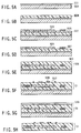
- a first example shows a method for manufacturing an optoelectric wiring substrate 50, which is shown in FIG. 2A. This method will be described below with reference to FIGS. 5A to 5O.
- FIGS. 5A to 5O show each step of the method for manufacturing the optoelectric wiring substrate 50 and are arranged in the order of the steps.
- a thin film layer of Cr and Cu is sputtered as a release layer 531 on a support substrate 559 that is a silicon wafer, and about 10 ⁇ m of Cu layer is subsequently formed thereon in a copper sulfate plating bath.
- Polyimide OPI-N1005 (manufactured by Hitachi Chemical Industry Inc.) is spin-coated on the release layer 531 as a first clad 504 and imidized at 350°C.
- the film thickness is, for example, about 20 ⁇ m.
- Polyimide OPI-N1305 (manufactured by Hitachi Chemical Industry Inc.) is similarly spin-coated on the first clad 504 as a core layer 532 and imidized at 350°C.
- the film thickness is, for example, about 8 ⁇ m.
- the materials of the core 501 (core layer 532) and the first clad 504 (the clad 503), which constitute an optical wiring layer 51, need not necessarily be the polyimide resins.
- the materials may be polymeric materials such as fluorinated or deuterated epoxy resins, ester methacrylate resins, or the like which are subject to fewer losses in the wavelength of light used for optical signals.
- Al is deposited on a surface of the core layer 532, a predetermined photo resist pattern is formed, and Al metal masks 533 and 535 are formed by means of etching.
- the metal mask 533 corresponds to a pattern of a core 501 that will be an optical wiring.
- the metal mask 535 corresponds to a pattern of alignment marks 507.
- an oxygen gas is used to etch the core layer 532 by means of reactive ion etching.
- the Al film which is the metal masks, is etched off to simultaneously form the pattern of the core 501 (optical wiring) and the pattern of the alignment marks 507.
- the line width of the core 501 pattern is, for example, 8 ⁇ m.
- its cross section is a square, for example, 8 ⁇ m in height and 8 ⁇ m in width.
- the size of the cross section of the core 501 are not limited to this but may be between 5 and 100 ⁇ m depending on differences in transmission mode and in refractive index between the core and the clad.
- a thin metal film of Cr and Cu is sputtered on a surface of the second clad 506.
- about 10 ⁇ m of a Cu layer is formed in a copper sulfate plating bath.
- a photo resist pattern is formed using the photolithography technique, and is etched using an etchant.
- pads 509, an electric wiring 513, and lands 511 can be formed.
- Previously formed openings 537 are shown with the lands 511 in FIG. 5E. Hole sections for forming via holes 523 are formed later in these openings 537 by means of a laser.
- pads, an electric wiring, and lands for connections with electric parts are formed.
- a photo resist 539 is coated as a protect film as shown in FIG. 5G. This film protects the pads, 509, electric wiring 513, and lands 511, which are formed of copper, from a release agent.
- the Cu layer in the release layer 531 is dissolved using a ferric chloride liquid as a release agent, and the optical wiring layer is released to produce an optical wiring film, as shown in FIG. 5H.
- the side of the optical wiring layer 51 on which the pads 509, the electric wiring 513, and the lands 511 are formed is stuck to a second support 541 using an adhesive.
- the second support 541 had better be transparent so that the alignment marks 507 can be seen from the side of the optical wiring layer 51 which is not stuck to the second support.
- the adhesive must be easy to release or be likely to have its adhesive strength reduced when hardened by means of ultraviolet rays.
- a mirror 34 is mechanically formed in part of the core 501 pattern at an angle of 45° relative to the substrate 52 using the alignment marks (refer to FIG. 4) as references.
- a modified polyimide resin exhibiting a thermal plasticity is coated and dried on the substrate 52 with the electric wiring 519. Then, the surface of the optical wiring layer on which the mirror has been formed is stuck to the substrate 52 and heated for adhesion.
- the structure is irradiated with ultraviolet rays to release the second support 541, as shown in 5L.
- a plated resist 543 is coated on the optical wiring layer 51 as a protect film, as shown in FIG. 5M.
- holes 545 for the via holes 523 are formed by means of a laser.
- suitable lasers include an excimer laser, a carbon dioxide laser, a YAG laser, etc.
- a thin metal film of Cr and Cu is sputtered on the surface of the optical wiring layer 51 and on internal surfaces of the laser-processed holes 545. Then, this thin metal film is used as an electrode to plate the inside of the via holes 523 and the land 511 sections with copper in a copper sulfate plating bath. Finally, the plated resist 543, which is a protect film, is removed, and the via holes 523 and the lands 511 are formed to obtain the optoelectric wiring substrate 50 shown in FIG. 2A.
- a second example of a method for manufacturing an optoelectric wiring substrate is another method for manufacturing the optoelectric wiring substrate 50 shown in FIG. 2A. This method will be described below with reference to FIGS. 6A to 6M.
- FIGS. 6A to 6M show each step of this method for manufacturing the optoelectric wiring substrate 50 and are arranged in the order of the steps.
- a thin film layer of Cr and Cu is sputtered as a release layer 531 on a substrate 52 that is a silicon wafer, and about 10 ⁇ m of Cu layer is subsequently formed thereon in a copper sulfate plating bath.
- Polyimide OPI-N1005 (manufactured by Hitachi Chemical Industry Inc.) is spin-coated on the release layer 531 as a first clad 504 and imidized at 350°C.
- the film thickness is, for example, about 20 ⁇ m.
- Polyimide OPI-N1305 (manufactured by Hitachi Chemical Industry Inc.) is similarly spin-coated on the first clad 504 as a core layer 532 and imidized at 350°C At this point, the film thickness is, for example, about 8 ⁇ m.
- the materials of the core 501 (core layer 532) and clad 503, which constitute an optical wiring layer, need not necessarily be the polyimide resins.
- the materials may be polymeric materials such as fluorinated or deuterated epoxy resins, ester methacrylate resins, or the like which are subject to fewer losses in the wavelength of light used for optical signals.
- Al is deposited on a surface of the core layer 532, and a predetermined photo resist pattern is formed and etched to form Al metal masks 533 and 535.
- the metal mask 533 corresponds to a pattern of a core 501 that will be an optical wiring.
- the metal mask 535 corresponds to a pattern of alignment marks 507.
- an oxygen gas is used to etch the core layer 532 by means of reactive ion etching.
- the Al film which is the metal masks, is etched off to simultaneously form the pattern of the core 501 (optical wiring) and the pattern of the alignment marks 507.
- the line width of the core 501 pattern is, for example, 8 ⁇ m.
- its cross section is a square, for example, 8 ⁇ m in height and 8 ⁇ m in width.
- the size of the cross section of the core 501 are not limited to this but may be between 5 and 100 ⁇ m depending on differences in transmission mode and in refractive index between the core and the clad.
- OPI-1005 is coated and imidized as a second clad 506. This step is similar to that for the first clad 504. At this point, the clad has a thickness of 20 ⁇ m, for example, on the core optical wiring layer.
- a mirror 505 is mechanically formed in part of the core 501 pattern at an angle of 45° relative to the substrate 52 using the simultaneously formed alignment marks (refer to FIG. 4) as references.
- the Cu layer in the release layer is dissolved using a ferric chloride liquid as a release agent, and the optical wiring layer is released to produce an optical wiring film, as shown in FIG. 6G.
- a modified polyimide resin exhibiting thermal plasticity is coated and dried on the substrate 52 with the electric wiring 519. Then, the surface of the optical wiring layer on which a mirror has been formed is stuck to the substrate 52 and heated for adhesion.
- holes 545 are formed by means of a laser.
- suitable lasers include an excimer laser, a carbon dioxide laser, a YAG laser, etc.
- a thin metal film 547 of Cr and Cu is sputtered on a surface of the optical wiring layer 51 and on internal surfaces of the laser-processed holes 545.
- a plated resist pattern 543 (protect film 549) is formed on the optical wiring layer surface except for pads 509, lands 511, and an electric wiring 513, as shown in FIG. 6K.
- the thin metal film 547 is used as an electrode to plate the inside of the via holes 523, the pads 509, the lands 511, and the electric wiring 513 with copper in a copper sulfate plating bath.
- the plated resist 543 is removed and the thin metal film 547 is further removed by means of soft etching. Then, the via holes 523, the pads 509, the lands 511, and the electric wiring are formed to obtain the optoelectric wiring substrate 50.
- a third example of a method for manufacturing an optoelectric wiring substrate is a method for manufacturing an optoelectric wiring substrate 53, which is shown in FIG. 2B. This method will be described below with reference to FIGS. 7A to 7P.
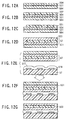
- FIGS. 7A to 7P show each step of the method for manufacturing the optoelectric wiring substrate 53 and are arranged in the order of the steps.
- a thin film layer of Cr and Cu is sputtered as a release layer 531 on a substrate 52 that is a silicon wafer, and about 10 ⁇ m of Cu layer is subsequently formed thereon in a copper sulfate plating bath.
- Polyimide OPI-N1005 (manufactured by Hitachi Chemical Industry Inc.) is spin-coated on the release layer 531 as a first clad 504 and imidized at 350°C.
- the film thickness is, for example, about 20 ⁇ m.
- Polyimide OPI-N1305 (manufactured by Hitachi Chemical Industry Inc.) is similarly spin-coated on the first clad 504 as a core layer 532 and imidized at 350°C.
- the film thickness is, for example, about 8 ⁇ m.
- the materials of the core 501 (core layer 532) and clad 503, which constitute an optical wiring layer, need not necessarily be the polyimide resins.
- the materials may be polymeric materials such as fluorinated or deuterated epoxy resins, ester methacrylate resins, or the like which are subject to fewer losses in the wavelength of light used for optical signals.
- Al is deposited on a surface of the core layer 532, and a predetermined photo resist pattern is formed and etched to form Al metal masks 533 and 535.
- the metal mask 533 corresponds to a pattern of a core 501 that will be an optical wiring.
- the metal mask 535 corresponds to a pattern of alignment marks 507.
- an oxygen gas is used to etch the core layer 532 by means of reactive ion etching.
- the Al film which is the metal masks, is etched off to simultaneously form the pattern of the core 501 (optical wiring) and the pattern of the alignment marks 507.
- the line width of the core 501 pattern is, for example, 8 ⁇ m.
- its cross section is a square, for example, 8 ⁇ m in height and 8 ⁇ m in width.
- the size of the cross section of the core 501 are not limited to this but may be between 5 and 100 ⁇ m depending on differences in transmission mode and in refractive index between the core and the clad.
- OPI-1005 is coated and imidized as a second clad 506. This step is similar to that for the first clad 504. At this point, the clad has a thickness of 20 ⁇ m, for example, on the core optical wiring layer.
- a thin metal film of Cr and Cu is sputtered on a surface of the second clad 506.
- about 10 ⁇ m of a Cu layer is formed in a copper sulfate plating bath.
- a photo resist pattern is formed using the photolithography technique, and is etched using an etchant.
- pads 509, an electric wiring 513, and lands 511 can be formed.
- Previously formed openings 537 are shown with the lands 511 in FIG. 7E. In these openings 535, hole sections for forming via holes 523 are formed later by means of a laser.
- pads, an electric wiring, and lands for connections with an electric part are formed.
- a photo resist 539 is coated as a protect film as shown in FIG. 7G. This film protects the pads, 509, electric wiring 513, and lands 511, which are formed of copper, from a release agent.
- the Cu layer in the release layer 22 is dissolved using a ferric chloride liquid as a release agent, and the optical wiring layer 51 is released to produce an optical wiring film, as shown in FIG. 7H.
- a side of the optical wiring layer 51 on which the pads 509, the electric wiring 513, and the lands 511 are formed is stuck to a second support 541 using an adhesive.
- the second support 541 had better be transparent so that the alignment marks 507 can be seen from its side to which the optical wiring layer 51 is not stuck.
- the adhesive must be easy to release or tend to have its adhesive strength reduced when hardened by means of ultraviolet rays.
- a thin film layer of Cr and Cu is sputtered on the surface of the optical wiring layer 51 opposite to its stuck surface, and 10 ⁇ m of a Cu layer is formed thereon in a copper sulfate plating bath.
- a photo resist pattern is formed using the photolithography technique, and is etched using an etchant to form a laser mask 551 for forming a mirror.
- the position of the laser mask 551 is defined by the alignment marks 507 similarly to the pads 509 on the opposite surface.
- openings 553 are formed in the laser mask. Accordingly, with irradiation with laser light, only the openings 553 are processed.
- suitable lasers include an excimer laser, a carbon dioxide laser, a YAG laser, etc.
- the laser mask 551 is removed using an etchant.
- a modified polyimide resin 521 exhibiting thermal plasticity is coated and dried on the substrate 52 with the electric wiring 519. Then, the surface of the optical wiring layer on which the mirror has been formed is stuck to the substrate 52 and heated for adhesion.
- the structure is irradiated with ultraviolet rays to release the second support 541, as shown in 7M.
- a plated resist 543 is coated on the optical wiring layer 51 as a protect film, as shown in FIG. 7N.
- holes 555 are formed by means of a laser.
- suitable lasers include an excimer laser, a carbon dioxide laser, a YAG laser, etc.
- a thin metal film of Cr and Cu is sputtered on the surface of the optical wiring layer 51 and on the inside of the laser-processed holes. Then, this thin metal film is used as an electrode to plate the inside of the via holes 523 and the lands 511 with copper in a copper sulfate plating bath. Furthermore, the plated resist 543, which is a protect film, is removed, and the via holes 523 and the lands 511 are formed to obtain the optoelectric wiring substrate 53.
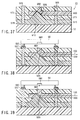
- a mirror can be formed by forming a laser mask for mirror formation and irradiating the mask with laser light with an incident angle of 45° relative to the substrate. This simplifies the steps and enables the positions of the pads and mirror to be accurately determined using the single photo mask.
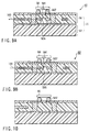
- a method 1-4 for manufacturing an optoelectric wiring substrate is a method for manufacturing an optoelectric wiring substrate 55, which is shown in FIG. 3A. The method will be explained referring to FIGS. 8A and 8B.
- the optoelectric wiring substrate 55 is formed by providing a resin layer 525 (having the same refractive index as the clad 503) on the optoelectric wiring layer 50 as described above.
- the fourth manufacturing method is the first manufacturing method with addition of new steps for manufacturing the resin layer 525. Description of the same steps as in the first manufacturing method is omitted below, and only the new additional steps will be explained.
- FIGS. 8A and 8B show the steps for manufacturing the resin layer 525 which are continued from FIG. 5O, and are arranged in the order of the steps.
- Polyimide OPI-N1005 manufactured by Hitachi Chemical Industry Inc.
- the film thickness is, for example, about 10 ⁇ m.
- the pads 509 are irradiated with laser light using the alignment marks 507 as references, thereby removing the polyimide from the pads 509. As a result, openings 556 are formed.
- preferable lasers include an excimer laser, a carbon dioxide laser, a YAG laser, etc.
- the optoelectric wiring substrate 55 can be obtained.
- the optoelectric wiring substrate 55, 57 can also be produced using the following method:
- the second and third manufacturing method include the additional steps wherein after completion of each optoelectric wiring substrate, the Polyimide OPI-N1005 (manufactured by Hitachi Chemical Industry Inc.) layer, which has been used for the clad 503, is formed on the optical wiring layer and the polyimide is then removed from the pads.
- a mounted substrate in which an optical part (a light-emitting element, a light-receiving element, or the like) is mounted on the optoelectric wiring substrate will be described below.
- the mounted substrate will be explained below by taking an optoelectric wiring substrate 55 by way of example, but this invention is applicable to other optoelectric wiring substrates.
- FIG. 9A shows a mounted substrate 60 in which a light-emitting element 58 is mounted on the optoelectric wiring substrate 55.
- a laser beam 100 emitted from a light-emitting surface 581 of a light-emitting element 131 is reflected by a mirror 505 and then propagates through a core 501 in an optical wiring layer 506.
- FIG. 9B shows a mounted substrate 62 in which a light-emitting element 59 is mounted on the optoelectric wiring substrate 55.
- the laser beam 100 which has propagated through the core 501 in the optical wiring layer 56, is reflected by the mirror 505 and then impinges on a light-receiving surface 591 of the light-receiving element 59.
- FIG. 10 shows the mounted substrate 62 in which a BGA package 66, an electric part, is mounted on an optoelectric wiring substrate .
- optical and electric parts and the optoelectric wiring substrate are electrically connected together using solder balls 557.
- the electric connection is made by soldering pads 509 and the optical part together.
- each of the above manufacturing methods enables the core 501 and alignment marks 507, 515 to be simultaneously formed. Then, the alignment marks 507, 515 can be used as references to accurately determine a position of the mechanically formed mirror 505 or a position of a mirror 512 formed using a laser mask.
- a self alignment effect of solder used for joining allows a position of the light-emitting or light-receiving surface of the optical part to be accurately determined.
- the optical part can be more accurately aligned during soldering of the solder balls or leads. That is, since soldering of the solder balls or leads are put in openings 556 accurately aligned based on the alignment marks 507, the optical part or the like mounted on the optoelectric wiring substrate can be more accurately aligned.
- the locational relationship between the core acting as the optical wiring, the pads installed an optical part or the like and the mirror can be extremely approximated to the design. This is because the optoelectric wiring substrate and mounted substrate according to the present invention have the above mentioned alignment effects to enable the optical axes of the optical part and the core acting as the optical wiring to be optically aligned easily.
- the optoelectric wiring substrate according to the present invention further enables the electric wiring to be formed on the optical wiring layer. Accordingly, cross talk between the electric wires can be restrained. As a result, noise can be reduced.
- the optical propagation loss of the core can be reduced.
- the reason is as follows: After being manufactured on the flat support, the optical wiring layer according to the present invention is stuck to the substrate with the electric wiring. Thus, the effect of recesses and projections of the electric wiring on the substrate can be lessened compared to an optical wiring layer directly manufactured on a substrate (with an electric wiring).
- the second embodiment can provide a higher alignment effect in manufacturing an optoelectric wiring substrate.
- a method in which a mirror 505, 512 for reflecting laser light is not formed is taken by way of example. Adding a known mirror formation step to the manufacturing method described below enables an optoelectric wiring substrate with a mirror to be manufactured easily.
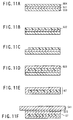
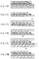
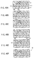
- FIGS. 11A to 11N A first example of a method for manufacturing an optoelectric wiring substrate according to second embodiment will be described with reference to FIGS. 11A to 11N
- the resulting optoelectric wiring substrate is a substrate 70, which is shown in FIG. 11N
- FIGS. 11A to 11N show each step of this manufacturing method and are arranged in the order of the steps.
- a thin film layer of Cr and Cu is sputtered as a release layer 531 on a first support substrate 559 that is a silicon wafer or the like, and about 1 ⁇ m of Cu layer is subsequently formed thereon in a copper sulfate plating bath.
- Polyimide OPI-N1005 manufactured by Hitachi Chemical Industry Inc.
- the film thickness is, for example, about 15 ⁇ m.
- the first support substrate 559 is not limited to a silicon wafer but may be a robust material having smooth surfaces and which can resist a high temperature of about 400°C.
- Polyimide OPI-N1305 (manufactured by Hitachi Chemical Industry Inc.) is similarly spin-coated on the first clad 504 as a core layer 532 and imidized at 350°C.
- the film thickness is, for example, about 8 ⁇ m.
- Al is deposited on a surface of the core layer 532, and a predetermined photo resist pattern is formed and etched to form aluminum metal masks. Further, as shown in FIG. 11C, an oxygen gas is used to etch part of the core layer 532 by means of reactive ion etching. Likewise, an oxygen gas is used to etch off the aluminum film to form a core 532 that will be an optical wiring. Simultaneously with the formation of the core 501, alignment marks (not shown) are formed on the core layer 532. These alignment marks act as references for sticking this substrate to an electric wiring substrate, which will be described below.
- OPI-N1005 is spin-coated on the core 501 as a second clad 506 and imidized.
- the film thickness of the second clad 506 newly formed on the core 501 is, for example, about 15 ⁇ m (which is the same as the film thickness of the clad layer 561 formed in the step shown in FIG. 11A).
- an optical wiring layer 67 can be obtained which consists of the core 501 and a clad 503, which buries the core 501.
- a ferric chloride is used to dissolve and remove a release layer 531 to release an optical wiring layer 67, as shown in FIG. 11E.
- An electric wiring 519 is formed on the top surface of the electric wiring substrate 52.
- the electric wiring 519 generates recesses and projections which correspond to a difference in height of about 18 ⁇ m on the top surface of substrate 52.
- the conventional manufacturing method directly forms the optical wiring layer on the surface of the electric wiring substrate 52. Consequently, the optical wiring layer is affected by the unevenness of the surface, resulting in reduced accuracy.
- the manufacturing method according to the present invention solves this problem by executing the steps described below.
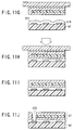
- a first adhesive 573 is coated on a second support substrate 541 made of glass, and the optical wiring layer 67 is stuck to the second support substrate 541 using a laminator.
- the laminator makes the surface of the optical wiring layer 67 very smooth.
- the second support substrate 541 may be any substrate made of glass or the like which has a certain level of strength and which is flat and transparent.
- the substrate is heated or irradiated with ultraviolet rays as required depending on the type of the adhesive.
- This manufacturing method uses a polyimide multilayer wiring substrate as the electric wiring substrate 52.
- the electric wiring 519 is formed on the top surface of the substrate 52.
- the electric wiring substrate 52 is not limited to the polyimide multilayer wiring substrate but may be a single-layer insulated substrate or a multilayer wiring substrate with electric wirings and insulated layers alternately laminated together.
- the material may be an insulated substrate comprised of a glass cloth impregnated with a resin, a polyimide film, or a ceramic substrate.
- a second adhesion layer 577 is formed on the electric wiring substrate 575.
- this layer can be formed by applying to the substrate a modified polyimide resin exhibiting thermal plasticity, followed by drying.
- a preferable material of the second adhesion layer 577 is a thermal plastic adhesive, for example, an ethylene-ester acrylate copolymer, a styrene-poly (metha) ester acrylate, a butyral resin, a polyamide-based resin, or a modified polyimide resin.
- a thermal plastic adhesive for example, an ethylene-ester acrylate copolymer, a styrene-poly (metha) ester acrylate, a butyral resin, a polyamide-based resin, or a modified polyimide resin.
- the range of sticking temperature is between 250 and 300°C, which is preferable in terms of the heat resistance of solder on an optoelectric wiring substrate.
- the optical wiring layer 67 must be released from the second support substrate 541 together with a first adhesion layer 573.
- the design of this structure must be such that the adhesion strength with which the second adhesion layer 577 adheres to the optical wiring layer 67 is larger than the adhesion strength with which the first adhesion layer 573 adheres to the optical wiring layer 67.
- Alignment marks are formed on the electric wiring substrate 52, which is coated with the second adhesion layer 577. These alignment marks are provided at positions corresponding to the alignment marks formed in the step corresponding to FIG. 11C. As shown in FIG. 11G, the alignment marks formed on the electric wiring substrate 52 are aligned with the corresponding alignment marks formed on the optical wiring layer 52 stuck to the second support substrate 541 (glass substrate), through the glass substrate, in order to determine the positions of theses alignment marks.
- the second support substrate 541 is the transparent glass substrate.
- the glass substrate and the optical wiring layer 67 allow visible light to permeate therethrough smoothly, and the first adhesion layer 573 has a sufficiently small thickness. Consequently, the alignment marks of the optical wiring layer 67 and electric wiring substrate 52 can be visually checked from the rear surface (the surface opposite to the stuck side) of the second support substrate 577.
- the structure is heated at 250°C for one hour while applying a pressure P thereto from the rear surface of the second support substrate 541.
- the adhesion can be carried out with a reduced atmospheric pressure as required. If the second adhesion layer 577 tends to be hardened when exposed to electron beams or the like, it can be stuck to the optical wiring layer by irradiating it with electron beams from the second support substrate 541.
- the second support substrate 541 is released from the optical wiring layer together with the first adhesion layer 573 to complete the sticking of the electric wiring substrate 52 and the optical wiring layer 67.
- optical wiring layer 67 can be stuck and fixed to the electric wiring substrate 52 while maintaining its smoothness and without being affected by the unevenness of the underlying electric wiring substrate 52. This can be achieved by the steps in FIGS. 11F to 11I.
- the remaining step forms pads for mounting an optical or electric part on the optical wiring layer 67 stuck to the electric wiring substrate 52 and via holes for electrically connecting the optical part with the electric wiring substrate.
- a laser is used to form a hole section 570 for via hole 523 formation using the alignment marks (not shown) on the electric wiring substrate 52.
- the method for forming the hole section 570 may be perforation using a carbon dioxide laser, a UV-YAG laser, an excimer laser, or dry etching such as reactive ion etching.
- the underlying electric wiring 519 acts as a stopper for the penetration.
- a sputter is used to form thin metal films (not shown) in the order of Cr and Cu. Furthermore, 10 ⁇ m of PMER (manufactured by Tokyo Applied Chemical Industry Co., LTd.) is coated on the films using a spin coater, and is then dried at 90°C to form a photo resist 541.
- PMER manufactured by Tokyo Applied Chemical Industry Co., LTd.
- a photo mask having a predetermined pattern is used to carry out exposure and development using as references the alignment marks (not shown) formed on the electric wiring substrate 52. Then, an opening 570 for via hole 523 formation and an opening 575 for pad formation are produced. Further, post-baking is executed at 110°C.
- the thin metal films are used as a negative electrode to form a plated film 576 in a copper sulfate bath.
- the plated film 576 is, for example, 10 ⁇ m in thickness, which is substantially equal to the thickness of the photo resist.
- the photo resist 571 is removed by means of an exclusive release agent, and the thin metal films are dissolved and removed by means of an etchant to produce via holes 523 and pads 519.
- an optoelectric wiring substrate 70 according to the present invention can be completed.
- This method is an another method for manufacturing the optical wiring layer on the transparent support substrate, which is similar to the manufacturing method 2-1.
- the resulting optoelectric wiring substrate is a substrate 70, which is shown in FIG. 11N.
- FIGS. 12A to 12G show each step of the sixth manufacturing method and are arranged in the order of execution.
- an optical wiring layer is manufactured.
- a thin film layer of Cr and Cu is sputtered on a third support substrate 584 made of glass or the like, to form a release layer 563 as shown in FIG. 12A.
- the third support substrate 584 is not limited a glass substrate but may be any robust substrate that has smooth surfaces, that can resist a temperature of about 400°C, and that allows visible light to permeate therethrough smoothly. These characteristics are common to a second substrate 541.
- a Cu layer is formed in a copper sulfate plating bath (not shown).
- the photo etching method a specified method, is used to form alignment marks (not shown) at predetermined positions of this thin metal film layer.
- the alignment marks are used as alignment references in sticking the optical wiring layer to an electric wiring substrate, which will be described below.
- Polyimide OPI-N1005 (manufactured by Hitachi Chemical Industry Inc.) is similarly spin-coated on the Cu layer and imidized at 350°C to form a clad 504 as shown in FIG. 12A.
- the clad 504 has a thickness, for example, of about 15 ⁇ m.
- Polyimide OPI-N1305 (manufactured by Hitachi Chemical Industry Inc.) is similarly spin-coated on the clad layer 561 and imidized at 350°C to form a core layer 532 as shown in FIG. 12B.
- the core layer 532 has a thickness, for example, of about 8 ⁇ m.
- Polyimide OPI-N1005 is similarly coated on the core 501 and part of the clad 504 and imidized at 350°C to form a clad 503, which buries the core 501.
- the clad layer newly laminated in this step has a thickness of 15 ⁇ m, for example, on the core 501.
- a second adhesion layer 577 is formed on an electric wiring substrate 52.
- this layer can be formed by applying to the substrate a modified polyimide resin exhibiting thermal plasticity, followed by drying.
- a preferable material of the second adhesion layer 577 is a thermal plastic adhesive, for example, an ethylene-ester acrylate copolymer, a styrene-poly (metha) ester acrylate, a butyral resin, a polyamide-based resin, or a modified polyimide resin.
- a thermal plastic adhesive for example, an ethylene-ester acrylate copolymer, a styrene-poly (metha) ester acrylate, a butyral resin, a polyamide-based resin, or a modified polyimide resin.
- the range of sticking temperature is between 250 and 300°C, which is preferable in terms of the heat resistance of solder on an optoelectric wiring substrate.
- Alignment marks are formed on the electric wiring substrate 52, which is coated with the second adhesion layer 577. These alignment marks are provided at positions corresponding to the alignment marks formed in the step corresponding to FIG. 12C. As shown in FIG. 12E, the alignment marks formed on the electric wiring substrate 52 are aligned with the corresponding alignment marks formed on the optical wiring layer stuck to the second support substrate 541 (glass substrate), through the glass substrate, in order to determine the positions of theses alignment marks.
- a third support substrate 584 has characteristics similar to those of the second support substrate 541 described in the fifth manufacturing method. Accordingly, alignment between the optical wiring layer 67 and the electric wiring substrate 52 can be executed easily.
- the structure is heated at 250°C for one hour while applying a pressure P thereto from a rear surface (a surface opposite to the stuck side) of the third support substrate 584.
- the adhesion can be carried out with a reduced atmospheric pressure as required. If the second adhesion layer 577 tends to be hardened when exposed to electron beams or the like, it can be stuck to the optical wiring layer by irradiating it with electron beams from the third support substrate 584.
- the release layer 531 is dissolved and removed by means of a ferric chloride liquid to release the third support substrate 584, as shown in FIG. 12G.
- This manufacturing method 2-2 enables an optoelectric wiring substrate 70 to be obtained.
- the optical wiring layer 67 can also be stuck and fixed to the electric wiring substrate 52 while maintaining the smoothness of the third support substrate 584 and without being affected by the unevenness of the electric wiring substrate 52.
- the optical wiring layer of the optoelectric wiring substrate is not affected by the unevenness of the underlying electric wiring substrate surface.
- the propagation loss of optical signals can be minimized. This is because the optical wiring layer is fixed to the smooth support substrate so as to be stuck to the electric wiring substrate while maintaining its smoothness.
- each of the support substrates is comprised of a transparent material.
- the electric wiring can be accurately aligned with pads for mounting an optical part.
- a mounted substrate in which an optical part (a light-emitting element, a light-receiving element, or the like) is mounted on the optoelectric mounted substrate 70 described in the second embodiment can be manufactured using steps similar to those of the mounted-substrate manufacturing method already described in the first embodiment.
- the third embodiment describes another type of optoelectric wiring substrate and a manufacturing method therefor.
- An important point of the optoelectric wiring substrate shown in the third embodiment is the concept that an optical wiring layer on which an optical part (optical element) is mounted is laminated on a substrate having an electric wiring, as in the first embodiment.
- an important point of the manufacturing method shown in the third embodiment is the concept that a core acting as an optical wiring, a pad pattern, and alignment marks are simultaneously manufactured.
- FIG. 13 shows a top view showing an optoelectric wiring substrate 70 according to the third embodiment as seen from an optical part-mounted side.
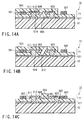
- FIG. 14A is a sectional view taken along the direction C-C in FIG. 13.
- FIG. 14C is a sectional view taken along the direction D-D in FIG. 13.
- a configuration of the optoelectric wiring substrate 70 will be described in the order of an optical wiring system, an electric wiring system, and connections between the optical and electric wiring systems.
- An optical wiring layer 71 consists of a core 501 through which optical signals propagate and a clad 503 that confines optical signals in the core 501.
- Optical signals propagate through the core 501 by increasing the refractive index of a material forming the core 501 above that of the clad 503.
- the core 501 has a mirror 505 installed in such a manner that optical signals are incident at 45°.
- Optical signals propagate between optical waveguides and an optical part (a laser diode or a photo diode) via a mirror 505 (see FIGS. 20A and 20B).
- An interface of the mirror 505 is brought in contact with a resin having a lower refractive index than the core 501 or with air.
- a thin metal film may be formed on the interface.
- An optoelectric wiring substrate 72 which is shown in FIG. 14B, shows an example having another mirror 512 installed in such a manner that optical signals are incident at 45°.
- the optoelectric wiring substrates 70 and 52 have the same configuration except for formation of the mirror 512.
- the optical wiring layer 71 has a second core 502 that is not used as an optical wiring.
- Pads 509, lands 511, and an electric wiring 513 are provided on the second core 502 in such a manner as to be arranged immediately above the mirror 505 and in a periphery thereof.
- the number and shape of the pads 509 is as described in the first embodiment.
- the substrate 52 has an electric wiring on its surface and its type and material are as described in the first embodiment.
- the optical wiring layer 71 is fixed to the substrate 52 via an adhesive 521.
- the optical part and the electric wiring 519 which are both provided on the optical wiring layer 51, are electrically connected together as follows:
- the lands 511 and the electric wiring 519 are electrically connected together via the via holes 523.
- a current from the electric wiring 519 is supplied to the lands 511 via the via holes 523 and further to the pads 509 via the electric wiring 513.
- the optical part provided on the optical wiring layer 71 can obtain a required current by means of electric connections with the pads 509.
- an electric part and the electric wiring on the substrate are similarly electrically connected together.
- the pads 509, the lands 511, and the electric wiring 513 are exposed from a surface of the optical wiring layer 71.
- optoelectric wiring substrates 74, 76 are shown in FIGS. 16A and 16B wherein the lands 511 and electric wiring 513 on the surface of the optical wiring layer 71 are coated with a resin layer 525 having the same refractive index as the clad 503 and wherein only part of the pad 509 for electric connections with the optical part is exposed.
- Each of the optoelectric wiring substrates 70, 72, 74, 76 has alignment marks 507 formed thereon for determining the positions of the pads 509 for mounting the optical part and alignment marks 515 for determining the position of the mirror 505. These alignment marks are formed simultaneously with the core 501 and the pad 509 pattern (that is, the second core 502) as described below.
- the alignment marks 515 may be provided as required. If, for example, alignment marks 515 are not formed, the surface of the optoelectric wiring substrate 70 on which the optical part is mounted is as shown in FIG. 4.
- an optical wiring layer is produced on a support substrate that is separate from a substrate having an electric wiring.
- This step is characterized by the following two points: A first point is that an optical wiring is formed by means of dry etching using a metal mask, whereas an optical wiring pattern, pads, and alignment marks are simultaneously formed using the photolithography technology. A second point is that a metal film constituting the metal mask is also used as a pad conductor film.
- a mirror is formed in part of the core using the alignment marks as references.
- the optical wiring layer thus manufactured is stuck to the substrate having an electric wiring.
- pads for installing an optical part or the like are electrically connected with the electric wiring substrate through via holes.
- the method comprises the step of producing beforehand the optical wiring layer on the support separate from the electric wiring substrate and the step of sticking this layer to the electric wiring substrate. Due to these steps, the optical wiring layer serves to lessen the effect of recesses and projections on the underlying electric wiring substrate, thereby reducing the loss of optical signals arising from this unevenness.
- FIGS. 13 and 14A show an optoelectric wiring substrate 74 that is finally obtained in this method.
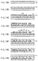
- FIG. 17A to 17P show each step of the method for manufacturing the optoelectric wiring substrate 70 and arranged in the order of the steps.
- a thin film consisting of Cr and Cu and constituting a release layer 531 is formed by a sputtering method on a silicon wafer constituting a first support substrate 559, followed by forming a Cu layer (not shown) within a copper sulfate plating bath in a thickness of about 10 ⁇ m, as shown in FIG. 17A.
- OPI-N1005 (trade name of a polyimide manufactured by Hitachi Kasei Kogyo K.K.) is spin-coated on the release layer 531, followed by conversion into imide at 350°C for forming a first clad 504, as shown in FIG. 17B.
- the thickness of the first clad 504 is, for example, 20 ⁇ m.
- OPI-N1305 (trade name of polyimide manufactured by Hitachi Kasei K.K.) is spin-coated on the first clad 504, followed by conversion into imide at 350°C to form a core layer 532, as shown in FIG. 17C.
- the thickness of the core layer 532 is, for example, 8 ⁇ m.
- the materials of the core layer 532 and the clad 504 used in the optical wiring layer 71 are not limited to polyimide resins.
- polyimide resins for example, it is possible to use fluorinated or deuterated epoxy resins, methacrylic acid ester resins or the like which are subject to fewer losses in the wavelength of light used for optical signals.
- Cr and Cu are sputtered on the core layer 532, followed by forming a Cu plating film (not shown) by using a copper sulfate plating bath.
- the thickness of the Cu plated film is, for example, 10 ⁇ m.
- a predetermined photoresist pattern is formed, followed by performing an etching treatment to form Cr/Cu metal masks 534 and 536.
- the metal mask 534 corresponds to a pattern of the core 501 forming an optical wiring.
- the metal mask 536 corresponds to a pattern of an alignment mark 507. Also, a pattern of pads, lands and electric wiring, which are not shown in the drawing, is formed similarly.
- the core layer 532 is etched by a reactive ion etching using an oxygen gas to form a core 501 as shown in FIG. 17D.
- a photoresist coating was applied, followed by light exposure and development to expose the metal mask (not shown) on the core pattern acting as an optical wiring, as shown in FIG. 17E. Further, the exposed metal mask is removed by etching.
- the line width of the core pattern was 8 ⁇ m, and the core pattern was found to be square (8 ⁇ m ⁇ 8 ⁇ m) in cross section. It is possible for the cross sectional size to be determined appropriately to fall within a range of between 5 ⁇ m square and 100 ⁇ m square depending on the transmission mode and the refractive indexes of the core and the clad.
- the metal mask positioned on the pad 509, the electric wiring 513 and the land 511 is used as it is as a conductive layer conducting electric signals.
- An opening 537 for forming a via hole is formed separately by a laser beam irradiation in the land 511.
- a pad, an electric wiring and a land are formed for connection to electric parts.
- a second clad 506 is formed by coating of OPI-1005, followed by conversion into imide.
- the thickness of the clad 506 is 20 ⁇ m on, for example, the core 501.
- a metal mask consisting of a thin Al film is formed by a photolithography technology on the surface of the second clad 506.
- a reactive ion etching was applied by using an oxygen gas to permit the clad to be left at least around the optical wiring (see FIG. 14), and a pattern of the clad 503 as shown in FIG. 17G was formed such that the Cu surface on the surface layer of the pad 509 was exposed to the outside.
- a photoresist 543 acting as a protective film was formed by coating in order to protect the pad 509 made of copper, the electric wiring 513 and the land 511 from the a releasing solution.
- the Cu layer in the release layer 531 was dissolved in the release solution containing ferric chloride so as to peel the optical wiring layer from the first support substrate 559.
- the second clad 506 was bonded to a second support substrate 541 by using an adhesive.
- the second support substrate 36 should be transparent such that an alignment mark 507 can be observed from the side on which the optical wiring layer is not bonded. It is desirable to use an adhesive that can be peeled off easily or that can be hardened upon irradiation with an ultraviolet light so as to decrease the adhesive strength.
- a mirror 505 making an angle of 45° with the substrate is formed by a mechanical processing in a part of the core 501 using as a criterion the alignment mark (not shown) formed simultaneously with formation of the pattern of the core 501 acting as an optical wiring.
- the substrate 52 is coated with a thermoplastic denatured polyimide resin 521 as an adhesive 521 in a thickness of 20 ⁇ m and, then, the coating is dried. Further, the polyimide resin 521 (adhesive 521) is attached to that surface of the optical wiring layer which is on the side of the mirror 505 so as to achieve bonding by heating.
- the optical wiring layer is peeled off the second support substrate 541 by irradiation with an ultraviolet light.
- the optical wiring layer is covered with a plating resist 543 as a protect film as shown in FIG. 17N.
- a hole 545 for a via hole 523 is formed by a laser irradiation in the opening portion 537 of the land.
- An excimer laser, a carbon dioxide gas laser, a YAG laser, or the like is suitable for use as the laser.
- a metal thin film of Cr and Cu is formed by a sputtering method on the surface of the optical wiring layer and within the hole having a laser processing applied thereto. Then, a copper plating is applied within the via hole 523 and the land 511 within a copper sulfate bath using the metal thin film as an electrode. Further, the plating resist 543 acting as a protective film is removed to form a via hole 523 and a land 511.
- the optoelectric wiring substrate 74 can be obtained through the manufacturing steps described above.
- the optoelectric wiring substrate 72 shown in FIG. 14B differs from the optoelectric wiring substrate 70 in only the mirror formation. Therefore, the following description covers only the different steps while omitting the common steps.
- FIGS. 18A to 18C show the steps following the step shown in FIG. 17J.
- a thin film of Cr and Cu is formed by a sputtering method on the first clad 504, as shown in FIG. 18A.
- a Cu layer is formed within a copper sulfate bath in a thickness of about 10 ⁇ m.
- a photoresist pattern is formed by a photolithography technology, followed by etching with an etchant to form a mask 551 for a laser for forming a mirror.
- An opening 553 is formed in the mask 551 for the laser. The opening 553 alone can be processed by irradiation with a laser beam. The position of the mask for the laser is defined by the alignment mark 507.
- the mask 551 for the laser is irradiated with a laser beam such that the angle made between the substrate surface and the laser beam is set at 45° so as to form a mirror 512 making an angle of 45° with the substrate.
- An excimer laser, a carbon dioxide gas laser, a YAG laser, or the like is suitable for use as the laser.
- the mask 551 for the laser is removed with an etchant, as shown in FIG. 18C.
- the substrate 52 having an electric wiring 519 formed thereon is coated with a thermoplastic denatured polyimide resin 521 used as an adhesive in a thickness of 20 ⁇ m. Then, the coating is dried, and the mirror-formed portions of the optical wiring layer are bonded to each other under heating.
- a method 3-3 of manufacturing an optoelectric wiring substrate 74 shown in FIG. 16A will now be described.
- the optoelectric wiring substrate 74 differs from the optoelectric wiring substrate 70 in two aspects. First of all, pads 509, lands 511 and electric wirings 513 formed are covered with the clad 503. Also, the clad 503 has a different pattern. It follows that the steps for patterning the clad 503 employed in method 3-1 can also be employed in method 3-3. Also, the steps for forming the resin layer 525 is newly added in method 3-3. The steps shown in FIGS. 19A to 19F are equal to those in method 3-1 and, thus, the description thereof is omitted.
- FIGS. 19G and 19O show the steps newly employed in method 3-3, which follow the step shown in FIG. 17E.
- the Cu layer in the release layer 531 was dissolved in the release solution containing ferric chloride so as to peel the optical wiring layer from the first support substrate 559.
- the second clad 506 was bonded to a second support substrate 541 by using an adhesive.
- the second support substrate 36 should be transparent such that an alignment mark 507 can be observed from the side on which the optical wiring layer is not bonded. It is desirable to use an adhesive that can be peeled off easily or that can be hardened upon irradiation with an ultraviolet light so as to decrease the adhesive strength.
- a mirror 505 making an angle of 45° with the substrate is formed by a mechanical processing in a part of the core 501 using as a criterion the alignment mark (not shown) formed simultaneously with formation of the pattern of the core 501 acting as an optical wiring.
- the substrate 52 is coated with a thermoplastic denatured polyimide resin 521 as an adhesive 521 in a thickness of 20 ⁇ m and, then, the coating is dried. Further, the polyimide resin 521 (adhesive 521) is attached to that surface of the optical wiring layer which is on the side of the mirror 505 so as to achieve bonding by heating.
- the optical wiring layer is peeled off the second support substrate 541 by irradiation with an ultraviolet light.
- the optical wiring layer is covered with a plating resist 543 as a protect film as shown in FIG. 17N.
- the optical wiring layer is peeled off the second support substrate 541 by irradiation with an ultraviolet light.
- the optical wiring layer is covered with a plating resist 543 as a protect film as shown in FIG. 19L.
- a hole 545 for a via hole 523 is formed by a laser irradiation in the opening portion 537 of the land.
- An excimer laser, a carbon dioxide gas laser, a YAG laser, or the like is suitable for use as the laser.
- a hole 537 for forming a via hole 523 is formed, followed by forming a thin film of Cr and Cu by a sputtering method on the surface of the optical wiring layer 75 and within the hole having a laser processing applied thereto. Then, a copper plating is applied to the inner region of the via hole 523 and to the land 513 within a copper sulfate bath using the metal thin film as an electrode. Further, the plating resist, which is the protective film 543, is removed to form the via hole 523.
- the second clads 506 on the pads 509 are removed by laser processing using the alignment mark 507 as a criterion so as to expose the surface of the Cu plating and form holes 508.
- An excimer laser, a carbon dioxide gas laser, a YAG laser or the like is suitable for use as the laser.
- the optoelectric wiring substrate 74 can be obtained by the steps described above.
- the method of manufacturing the optoelectric wiring substrate 74 it is possible to form a metal mask for a laser processing on the optical wiring layer 71, followed by applying a laser processing, in place of applying a mechanical processing to the mirror 512, thereby manufacturing the optoelectric wiring substrate 76 shown in FIG. 16B.
- a mounting substrate having optical parts such as a light-emitting device and a light-receiving device and an electric part mounted to the optoelectric wiring substrate 70, 72, 74 or 76 obtained by the example of the present invention can be obtained by the method similar to that of the first embodiment. As a result, a mounting substrate as shown in FIGS. 20A, 20B and 21 can be obtained.
- An important point of the optoelectric wiring substrate shown in forth embodiment is the concept that an absorption layer is provided between the optical wiring layer 82 and the substrate 52 for absorbing unevenness of the electric wiring 519.
- FIG. 22 shows a top view showing an optoelectric wiring substrate 80 as seen from an optical part-mounted side.
- FIG. 23 is a sectional view taken along the direction C-C in FIG. 22.
- the electric wiring 519 is formed on the substrate 52.
- An absorption layer 613 absorbs unevenness of the electric wiring 519. According to this configuration, the optoelectric layer 82 is not affected by unevenness of the electric wiring 519.
- the absorption layer 613 is comprised of a material having plasticity, elasticity, or both.
- a plastic absorption layer is called a "smooth layer”
- an elastic absorption layer is called a "cushion layer”.
- a plastic and elastic adhesive is used to stick the optical wiring layer 82 to the substrate 52, so that the adhesive forms an adhesion layer also acting as an absorption layer.
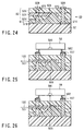
- first clad 504 and the second clad 506 and 4 may be reversed, as shown in FIG. 24, depending on formation of an optical and electric wiring layers.
- a substance constituting the first clad 504 may or may not be the same as a substance constituting the second clad 506.
- the second clad 506 in FIG. 24 is not necessarily flat and may even be absent.
- FIG. 25 is a sectional view showing that leads 582 from a light-emitting element 58 such as a semiconductor laser are soldered to the pads 509.
- a laser beam 100 emitted from a light-emitting surface 581 of the laser light-emitting element 58 is reflected by a mirror 505 and then propagates through the core 501.
- FIG. 26 is a sectional view showing that leads from a laser light-receiving element 59 such as a photo diode are soldered to the pads 509.
- a laser beam 100 propagating through the core 501 is reflected by the mirror 505 and is then incident on a light-receiving surface 591 of the light-receiving element 59.
- pads 510 for soldering an electric part or an electric wiring may be provided on the optical wiring layer of the optoelectric wiring substrate.
- the pads 510 for an electric part may be electrically connected to the electric wiring 519 on the substrate 52 through via holes 523.
- the pads 510 may be connected only to the electric wiring on the optical wiring layer 82 but not to the electric wiring 519 on the substrate 52. In this case, of course, no via hole 523 exists which electrically connects the pad 510 to the electric wiring on the substrate 52.
- an optical wiring layer 82 is produced on a support substrate which is separated from the substrate 52 having the electric wiring 519.
- a mirror is formed in part of a core.
- the optical wiring layer 82 is stuck to the electric wiring of the substrate 52 via the absorption layer 613.
- pads are produced which are electrically connected to the electric wiring 519 on the substrate through the via holes 523.
- An import point of this manufacturing method is that the method comprises the step of stucking to the electric wiring of the substrate 52 via the absorption layer 613
- a method 4-1 for manufacturing an optoelectric wiring substrate will be explained by focusing on pads 509 for an optical part which are electrically connected to an electric wiring 519 on a substrate 52 via the via holes 523.
- FIGS. 27A to 27Q show each step of the method for manufacturing the optoelectric wiring substrate 80 and arranged in the order of the steps.
- a release layer 531 is formed on a first support substrate 559.
- the first support substrate 559 must be heat-resistant and robust and have a thermal expansion coefficient equal or close to that of an optical wiring layer.
- a first clad 504 is formed on the release layer 531.
- a core layer 532 is formed on the first clad 504, and a core 501 through which light propagates and an alignment mark 507 for alignment are simultaneously produced using the photolithography technology as shown in FIG. 27C.
- the resulting locational relationship between the core 501 and the alignment mark 507 is very close to an intended one.
- the core 501 and the alignment mark 507 are covered with an second clad 506.
- FIG. 27E show lands 511, pads 510 for an electric part, and an electric wiring 513.
- a release agent protect film 539 is formed, as shown in FIG. 27F, to protect the lands 511, pads 510 for an electric part, and electric wiring 513 produced on the optical wiring layer.
- the structure is immersed in a release agent to dissolve the release layer 531, and the optical wiring layer is released from the first support substrate 559 to produce an optical wiring layer such as that shown in FIG. 6G.
- the protect film 539 is removed to obtain an optical wiring layer 82 such as that shown in FIG. 27H.
- a side of the optical wiring layer 82 on which the lads 511, the pads 510 for an electric part, and the electric wiring 513 are formed is stuck to a second support 541 using an adhesive.
- the second support 541 must be transparent so that the alignment mark 507 can be seen from its side to which the optical wiring layer 82 is not stuck.
- the adhesive must be easy to release or have a thermosetting or an ultraviolet-hardening property.
- a groove is formed in the optical wiring layer by means of dicing to form a mirror 505, as shown in FIG. 27J.
- the mirror 505 side of the optical wiring layer 82 is stuck via an absorption layer 613 to a side of the substrate 52 which has an electric wiring 519.
- the absorption layer 613 is produced on the substrate 52 before the optical wiring layer 82 is stuck thereto or the absorption layer 613 is produced on the mirror 505 side of the optical wiring layer before it is stuck to the substrate 52.
- the absorption layer 613 may be a smooth or cushiony layer or have both of these properties, but it is preferably an adhesion layer comprised of an adhesive having both properties.
- the second support substrate 541 is released from the optical wiring layer 82. If an thermosetting or ultraviolet-hardening adhesive has been used to stick the second support substrate 541 and the optical wiring layer 82 together, the second support substrate 541 is peeled off after being hardened by means of heat or ultraviolet rays, respectively.
- a hole 66 for forming a via hole is formed in the optical wiring layer by means of a laser.
- a thin chromium film is sputtered on the surface of the hole 66 and a surface of the optical wiring layer which is opposed to the substrate 52, and then a thin copper film is also sputtered on the thin chromium film.
- a protect film 543 is coated on the surface of the optical wiring layer 82 as shown in FIG. 27N.
- the thin copper film formed on the surfaces of the hole 545 and optical wiring layer is used as an electrode to electroplate the copper in order to produce a pad 509 and a via hole 523 for an optical part, as shown in FIG. 27O.
- the protect film 543 is removed. Subsequently, the thin chromium and copper films formed on the surface of the optical wiring layer are removed by means of soft etching to obtain an optoelectric wiring substrate 80 such as that shown in FIG. 27Q.
- An another method 4-2 for manufacturing an optoelectric wiring substrate will be explained by focusing on pads 509 for an optical part which are electrically connected to an electric wiring 519 on a substrate 52 via the via holes 523.
- FIGS. 28A to 28L show each step of the method for manufacturing the optoelectric wiring substrate 80 and arranged in the order of the steps.
- a release layer 531 is formed on a first support substrate 559.
- a first clad 504 is formed on the release layer 531.
- a core layer 532 is formed on the first clad 504, and a core 501 through which light propagates alignment marks 507 for alignment are simultaneously produced using the photolithography technology as shown in FIG. 28C.
- the resulting locational relationship between the core 501 and the alignment marks 501 is very close to an intended one.
- the core 501 and the alignment mark 507 are covered with an second clad 506.
- a groove is formed in the optical wiring layer by means of dicing to form a mirror 505, as shown in FIG. 28E.
- the structure is immersed in a release agent to dissolve the release layer 531, and the optical wiring layer is released from the first support substrate 559 to obtain an optical wiring layer 82 such as that shown in FIG. 28F.
- a mirror 505 side of the optical wiring layer is stuck via an absorption layer 613 to a side of the substrate 52 which has an electric wiring 519.
- the absorption layer 613 is produced on the substrate 52 before the optical wiring layer is stuck thereto or the absorption layer 613 is produced on the mirror 505 side of the optical wiring layer before it is stuck to the substrate 52.
- the absorption layer 613 may be a smooth or cushiony layer or have both of these properties, but it is preferably an adhesion layer comprised of an adhesive having both properties.
- a hole 545 for forming a via hole 523 is formed in the optical wiring layer by means of a laser.
- a thin chromium film is sputtered on the surface of the hole 545 and a surface of the optical wiring layer which is opposed to the substrate 52, and then a thin copper film is also sputtered on the thin chromium film.
- a resist 554 (protect film 539) is coated on the surface of the optical wiring layer 82 as shown in FIG. 28I.
- a photo mask is aligned using the alignment mark 507 as a reference, and the resist 539 is exposed via this photo mask and then developed in such a manner that only a portion of the resist 539 is removed on which pads and an electric wiring are to be produced, as shown in FIG. 28J.
- the thin copper film formed on the surfaces of the hole 545 and optical wiring layer is used as an electrode to electroplate the copper in order to produce a pad 509 for an electric part, an electric wiring 513, a via hole 523, and the pad 510 for an electric part, as shown in FIG. 28K.
- the resist 539 is removed, subsequently, the thin chromium and copper films formed on the surface of the optical wiring layer 82 are removed by means of soft etching to obtain an optoelectric wiring substrate such as that shown in FIG. 28L.
- Another method 4-3 for manufacturing an optoelectric wiring substrate 83 (see FIG. 29P) will be explained by focusing on pads 509 for an electric part which are electrically connected to an electric wiring 519 via the via holes 523.
- FIG. 29A to 29P show each step of the method for manufacturing the optoelectric wiring substrate 83 and arranged in the order of the steps.
- a release layer 531 is formed on a first support substrate 559.
- the first support substrate 559 must be heat-resistant and robust and have a thermal expansion coefficient equal or close to that of an optical wiring layer.
- a first clad 504 is formed on the release layer 531.
- a core layer 532 is formed on the first clad 504.
- a thin chromium film is sputtered on the core layer 532, and then a thin copper film is also sputtered on the chromium film to produce a thin metal film 540 consisting of two layers of the chromium film and the copper film.
- the thin metal film 540 is processed by means of the photolithography technology to produce metal masks.
- the metal masks include a metal mask 533 corresponding to the core 501 pattern and a metal mask 535 corresponding to a pattern of optical-part pads 509. Both patterns are simultaneously formed.
- a metal mask section may also be simultaneously formed which represents a pattern of pads 510 for an electric part and a pattern of an electric wiring 513.
- a portion of the core layer 532 which is not covered with the metal mask is removed by means of dry etching to remove the metal mask, that is, a core 501 is formed.
- the metal masks 533,535 are removed from the core 501, using the photolithography technology.
- An second clad 506 is coated as shown in FIG. 29H.
- the second clad 506 is removed from the optical-part pads 509, as shown in FIG. 29I.
- the optical-part pads 509 functions as a resist so as not to be affected by etching.
- a release agent protect film is formed on the second clad 506 and the optical-part pad 509. Then, the structure is immersed in a release agent, and the optical wiring layer is released from the first support 559. Further, the release agent protect film 531 is removed to obtain an optical wiring layer such as that shown in FIG. 29J.
- the optical-part pads 509 side of the electric wiring layer 84 is stuck to a second support substrate 541.
- the adhesive used must be easy to release or have a thermosetting or an ultraviolet-hardening property.
- a groove is formed in the optical wiring layer by means of dicing to form a mirror 505, as shown in FIG. 29L.
- the mirror 505 side of the optical wiring layer 84 is stuck via an absorption layer 613 to a side of the substrate 52 which has an electric wiring 519.
- the absorption layer 613 is produced on a substrate 115 before the optical wiring layer is stuck thereto or the absorption layer 613 is produced on the mirror 505 side of the optical wiring layer before it is stuck to the substrate 52.
- the absorption layer 613 may be a smooth or cushiony layer or have both of these properties, but it is preferably an adhesion layer comprised of an adhesive having both properties.
- the second support substrate 541 is released from the optical wiring layer 84. If an thermosetting or ultraviolet-hardening adhesive has been used to stick the second support substrate 541 and the optical wiring layer together, the second support substrate 541 is peeled off after being hardened by means of heat or ultraviolet rays, respectively.
- a hole 116 for forming via holes 545 is formed in a central portion of the optical-part pads 509 by means of a laser.
- the hole 545 is filled with copper by means of the semi-additive method to form via holes 523 and pads 509 electrically connected through the via holes 523 to the electric wiring 519 on the substrate 52, thereby obtaining an optoelectric wiring substrate.
- the second clad 506 may be omitted.
- the method is the same as the above manufacturing method except for the lack of the need to coat the second clad 506 or to remove the second clad 506 from the optical-part pad 509.
- Some conventional methods for optically coupling an optical part to an optical wiring provide a mirror in an optical wiring layer.
- FIG. 30 is a specific example described in Japanese Laid-Open Patent Publication (Kokai) No. 5-241044.
- a laser beam 307 propagating through an optical waveguide 301 is reflected by a mirror 303 and is then incident on a light-receiving surface 305 of a light-receiving element 304.
- FIG. 31 shows an example of an apparatus described in Japanese Laid-Open Publication (Kokai) No. 5-241044.
- This apparatus has a convex lens 308 on a surface of the waveguide 301 to converge the diffused laser beam 307 on the light-receiving surface 305, thereby increasing the optical coupling efficiency
- the optimal convex lens 308 varies depending on the relative locational relationship between a light-receiving element 304 and the optical waveguide 301 or the size of the light-receiving surface.
- different convex lenses 308 must be produced which correspond to each type of optical part, and this is cumbersome.
- this optoelectric wiring substrate is available for each of the optoelectric wiring substrates above mentioned.
- An important point of the optoelectric substrate shown in fifth embodiment is the concept that a new optical wiring layer, which propagates optical signals reflected by a mirror, is provided
- FIG. 32 is a sectional view of an optical wiring layer 87 of an optoelectric mounted substrate 86 according to a fifth embodiment (see FIGS. 37 and 38). First, the optical wiring layer 87 will be described with reference to these figures.
- the optical wiring layer 87 has a first core 600 extending parallel therewith and a second core 601 extending perpendicularly thereto. These cores constitute an optical wiring and are surrounded by a clad 23.
- An intersection between the first core 600 and the second core 601 includes a mirror 505 formed at 45° relative to the optical wiring layer.
- the interface of the mirror 505 is brought in contact with a resin having a lower refractive index than the second core 601 or with air.
- a reflecting layer comprised of a thin metal film 505 may be provided as in the optoelectric wiring substrate 81 shown in FIG. 33.
- optical signal propagates through the optical wiring layer as follows:
- FIG. 34 describes propagation of an optical signal (laser beam) through the optical wiring layer.
- a laser beam 100 propagating through the first core 600 is reflected by the mirror 505 and further propagates through the second core 602.
- the laser beam 100 diffuses after reflection from the mirror 505, it is confined in the core 601 and thus emitted from an end of the core 691 to an optical part (not shown) as a thin beam.
- FIGS. 35A to 35F sequentially show the steps of the manufacturing method.
- a release layer 531 is formed on a first support substrate 559.
- a layer 88 consisting of the first core 600 and the clad 603 is formed on the release layer 531 by means of the photolithography technology.
- a laser is used to form a hole 607 extending perpendicularly to a layer 82.
- the hole 607 is filled with the same material as the first core 600 to form the second core 601.
- grooves are formed at intersections between the first core 600 and the second core 601 by means of dicing.
- the release layer 531 is immersed in a release agent to release the optical wiring layer from the first substrate 559, thereby obtaining the optoelectric wiring layer 87 shown in FIG. 35F.
- FIGS. 36A to 36H sequentially show the steps of the manufacturing method.
- the release layer 531 is formed on the first support substrate 559.
- the layer 82 consisting of the first core 600 and the clad 603 is formed on the release layer 531 by means of the photolithography technology.
- a laser is used to form the hole 607 extending perpendicularly to the layer 88.
- the hole 607 is filled with the same material as the first core 600 to form the second core 601.
- a film 609 is coated on the layer 88.
- the film 609 may be replaced with a resist.
- Grooves 611 are formed by means of dicing as shown in FIG. 36F.
- the layer 88 is covered with a metal film 605 such as aluminum to produce the mirror 505.
- the film 609 is peeled off to release the metal film 605 except for the groove 607 portions. Further, the release layer 531 is immersed in a release agent to release the optical wiring layer from the first substrate 559, thereby obtaining the photoelectric wiring layer 81 shown in FIG. 39H.
- FIG. 37 is a sectional view taken along the first core 600 of the photoelectric mounted substrate 86 according to the fifth embodiment.
- the photoelectric wiring substrate 86 comprises the optical wiring layer 81 and an electric wiring substrate 52 stuck together via an absorption layer 519.
- the optical wiring layer 87 has pads, lands, an electric wiring, and via holes formed therein.
- An absorption layer 613 absorbs the unevenness of the electric wiring 519 to reduce the propagation loss of optical signals through the first and second cores 600 and 601.
- the absorption layer 67 must be comprised of a substance having plasticity, elasticity, or both.
- an absorption layer comprised of a plastic substance is called a "smooth layer”
- an absorption layer comprised of an elastic material is called a "cushion layer”.
- a plastic and elastic adhesive is used to stick the optical wiring layer to the substrate 52, so that the adhesive forms an adhesion layer also acting as the absorption layer.
- the absorption layer 613 is preferably a medium that is flexible enough to fill in the grooves 611 and that has a smaller refractive index than the cores. With these properties, the absorption layer 613 can not only fill the grooves 611 but also stick the optical wiring layer to the substrate.
- an end surface of the mirror 505 and the absorption layer 613 may be in contact with each other via a medium meeting the above conditions.
- a medium meeting the above conditions For example, air may be present between the end surface of the mirror 505 and the absorption layer 613 (because air meets the above conditions).
- pads for soldering an electric part or the electric wiring may be provided on the optical wiring layer 87 of this substrate 86.
- pads for an electric part may be electrically connected to the wiring on the substrate through via holes.
- the pads may be connected only to the electric wiring on the optical wiring layer but not to the electric wiring on the substrate. In this case, of course, no via hole exists which electrically connects the pad to the electric wiring on the substrate.
- FIG. 38 is a sectional view of the photoelectric wiring substrate 86 showing that leads from a laser light-emitting element 58 are soldered to pads 509.
- a laser beam 100 emitted from a laser light-emitting surface 581 of the laser light-emitting element 58 propagates through the second core 602, is reflected by the mirror 505, and then propagates through the first core 600.
- FIG. 39 is a sectional view showing that leads from a laser light-receiving element 59 are soldered to the pads 509.
- the laser beam 100 propagating through the first core 600 is reflected by the mirror 505, propagates through the second core 602, and is then incident on a light-receiving surface 591 of the light-receiving element 59.
- the laser beam 100 reflected by the mirror 505 diffuses but is confined in the second core 602, so that it is emitted from the end of the second core 602 as a thin beam and then efficiently impinges on the light-receiving surface 591.
- FIGS. 40A to 40H sequentially show the steps of the method for manufacturing the photoelectric wiring substrate 86.
- a mirror 505 side of the optical wiring layer 87 is stuck via an absorption layer 613 to an electric-wiring 519 side of a substrate 52.
- the absorption layer 613 is produced on the substrate 52 before the optical wiring layer is stuck thereto or the absorption layer 613 is produced on the mirror 505 side of the optical wiring 87 before it is stuck to the substrate 52.
- the absorption layer must have a smaller refractive index than cores.
- a hole 545 for forming a via hole is formed by means of a laser.
- a thin chromium film is sputtered on the surface of the hole 545 and a surface of the optical wiring layer 87 which is opposed to the substrate 52, and then a thin copper film is also sputtered on the thin chromium film.
- a resist 554 is coated on the surface of the optical wiring layer 87 as shown in FIG. 40C.
- the resist 554 is exposed via a photo mask and then developed in such a manner that only portions of the resist 554 on which pads and an electric wiring are to be provided are removed.
- the thin copper film formed on the surfaces of the hole 545 and optical wiring layer 87 is used as an electrode to electroplate the copper in order to produce a pad for an electric part 510, an electric wiring 513, a via hole 523, and a pad for an optical part 509, as shown in FIG. 40E.
- the resist 554 is removed. Subsequently, the thin chromium and copper films formed on the surface of the optical wiring layer 87 are removed by means of soft etching to obtain a photoelectric wiring substrate 86 such as that shown in FIG. 40F.
- a light-receiving element can be efficiently optically coupled to the optical wiring without the use of a converging convex lens.
- it is unnecessary to produce different converging convex lenses depending on the relative locational relationship between the light-receiving element and the optical wiring and the size of a light-receiving surface of the light-receiving element, resulting in easier manufacturing than with the conventional technique using a converging convex lens.
- the photoelectric wiring substrate can have a higher mounting density and a reduced size.
- the electric wiring can also be provided on the optical wiring layer, interference between the electric wires can be restrained.
- the absorption layer is provided to absorb the unevenness of the electric wiring on the substrate, thereby eliminating the propagation loss of optical signals.
- the sticking operation is performed precisely as intended.
- Optoelectric wiring substrates above mentioned mount an optical part or the like on only one of the surfaces.
- Optoelectric wiring substrate according to fifth embodiment can mount an optical part or the like on both of the surfaces
- An important point of the optoelectric substrate shown in sixth embodiment is the concept that a new optical wiring layer, which makes optical signals reflected by a mirror to propagate from one of the surfaces to the other surface, is provided
- FIG. 41 is a sectional view taken along the direction of light propagating in an optoelectric wiring substrate 90 according to the sixth embodiment. First, based on FIG. 41, a configuration of the optoelectric wiring substrate 90 will be described.
- a substrate 52 with an electric wiring 519 has a first optical wiring layer 620 on one of its surfaces (in FIG. 41, a top surface) which consists of a first clad 502, a second clad 506, and a core 501 surrounded by both clads.
- the substrate 52 has a second optical wiring layer on the other surface (in FIG. 41, a bottom surface) which consists of a first clad 504, a second clad 506, and a core 501 surrounded by both clads.
- the substrate 52 has an optical through-hole 624 penetrating the substrate 52 with the electric wiring in a vertical direction and consisting of a core 500 surrounded by the first clad 504.
- the optical through-hole 624 is made in the substrate 52 and extend vertically as shown in FIG. 41. Nonetheless, the optical through-hole is not limited to a vertical one in the present embodiment.
- the optical through-hole 624 need not be a vertical, so long as it can perform its essential function of guiding light from one surface of the substrate 52 to the other surface. For example, it may be a slant one, in which case the optical through-hole mirror 505 must be inclined at such an angle as to reflect the light into the optical through-hole 624.
- the core 501 of the first wiring layer 620, the core 500 of the optical through-hole 624, and the core 501 of the second wiring layer 622 all have an equal refractive index.
- One end of the core 500 of the optical through-hole 624 (in FIG. 41, an upper end) is connected to the core 501 of the first wiring layer 620, and in this connection area between the cores is formed a mirror 505 having a mirror surface inclined at 45° relative to the surfaces of the substrate 52.
- the other end of the core 500 of the optical through-hole 624 (in FIG. 41, a lower end) is connected to the second wiring layer 622, and in this connection area is formed a mirror 505 having a mirror surface inclined at 45° relative to the surfaces of the substrate 52.
- a conductor layer for electrically connecting these electric wiring layers may be formed as required on an inner surface 626 of a hole in the substrate through which the optical through-hole 624 is extended.
- a laser beam 100 that has propagated through the core 501 of the first wiring layer 620 is reflected by the upper mirror 505 and then propagates through the core 500 of the optical through-hole 624.
- the beam is then reflected by the lower mirror 505 and propagates through the core 501 of the second wiring layer 622.
- FIGS. 43A to 43J show each step of the method for manufacturing the photoelectric wiring substrate 90 and are arranged in the order of execution.
- a first through-hole 628 is formed in a substrate 52 having an electric wiring 519.
- Methods for forming the first through-hole 628 include a drill, a laser, RIE (Reactive Ion Etching), etc.
- an electric through-hole may be used as the through-hole 628.
- a dielectric layer is provided on an inner surface of the first through-hole 628 for electrically connecting these electric wiring layers together.
- a clad 630 is coated on both surfaces of the substrate 52 and on the inner surface of the first through-hole 628 in such a manner that the through-hole 22 is filled with the clad 630.
- a second through-hole 632 having a smaller inner diameter than the first through-hole 628 is formed in a central portion of the filled first through-hole 628.
- the second through-hole 632 is surrounded by the clad.
- Methods for forming the second through-hole 632 include a drill, a laser, RIE, etc.
- a core layer 532 is formed on both surfaces of the substrate 52 and on an inner surface of the second through-hole 632. As a result, the second through-hole 632 is filled with a core 500.
- the core layer 532 is covered with a metal film 634 on both surfaces of the substrate 52, as shown in FIG. 43E.
- the photolithography technology is used to remove unwanted portions of the metal film 634 which correspond to portions of the core layer 532 which are not used as an optical wiring.
- Both surfaces of the substrate 52 are etched by means of RIE to remove portions of the core 532 which are not covered with the remaining metal film 634, as shown in FIG. 43G.
- the remaining metal film 634 is removed from both surfaces of the substrate 52 as shown in FIG. 43H.
- a second clad 506 is coated on both surfaces of the substrate 52 as shown in FIG. 43I.
- Mirrors 505 each having a mirror surface inclined at 45° relative to the surfaces of the substrate 52 are formed in connections between the core parallel with the substrate 52 and the core perpendicular thereto, by means of dicing with a 90° cutting edge or RIE diagonal etching.
- the mirrors 505 may be mirrors 506 each formed with a metal reflecting film by means of sputtering or deposition.
- the optical wiring layers are provided on both surfaces of the substrate with the electric wiring and are optically connected together via the optical through-hole, thereby enabling a complicated optical wiring while allowing optical parts to be mounted on both surfaces of the substrate. Therefore, the optical wiring design can be simplified and high-density wiring and mounting can be achieved.
- the mirror in each of embodiments is formed so that light propagating through the optical wiring is incident thereon at 45°. Nonetheless, the angle of the mirror not limited to a vertical one. Accordingly, if a mirror having anther incident angle is formed, the optoelectric wiring substrate is designed corresponded to the angle (for example, an situation of pads 509, 510, an angle between the first core 600 and the second core 601, an angle of optical through-hole) so that passage through optical wave propagate can be formed arbitrary.
- a first clad (504) layer is formed on a smooth support substrate (559) via a release layer (531).
- a core (501) through which light propagates and alignment marks (507, 515) are simultaneously formed.
- these layers are covered with a second clad (506) to obtain an optical wiring layer (51).
- the optical wiring layer (51) is released from the support substrate (559) and stuck to a substrate (52) having an electric wiring (519).
- a mirror for reflecting light propagating through the core (501), pads (509, 510) for installing optical parts (58, 59)or the like, and via holes (523) for electrically connecting the electric wiring (519) on the substrate (52) to the pads (509, 510).
- the alignment marks (507, 515) are used as references.
Landscapes
- Physics & Mathematics (AREA)
- General Physics & Mathematics (AREA)
- Optics & Photonics (AREA)
- Engineering & Computer Science (AREA)
- Microelectronics & Electronic Packaging (AREA)
- Optical Integrated Circuits (AREA)
- Optical Couplings Of Light Guides (AREA)
Abstract
Description
Claims (36)
- An optoelectric substrate (50, 53, 55, 57) characterized by comprising a substrate (52) having an electric wiring (519) and an optical wiring layer (51,56) laminated on the substrate (52),said optical wiring layer (51,56) comprising:a core (501) through which light propagates;a clad (503) for holding said core (501);a mirror (505,512) for reflecting light propagating through said core (501);first conductive installation (509, 510) means formed on a surface of said optical wiring layer (51,56) for installing light-receiving means (59) for receiving light reflected by said mirror or light-emitting means (58) for emitting light toward said mirror (505,512); andconnection (523) means for electrically connecting said first conductive installation means (519) to said electric wiring.
- An optoelectric substrate (50, 53, 55, 57) characterized by comprising a substrate (52) having an electric wiring (519) and an optical wiring layer (51,56) laminated on the substrate (52),said optical wiring layer (51,56) comprising:a core (501) through which light propagates;a clad (503) for holding said core (501);a mirror (505, 512) for reflecting light propagating through said core (501);second conductive installation (509, 510) means formed on a surface of said optical wiring layer (51,56) for installing an electric part 66 (66); andconnection means (523) for electrically connecting said second conductive installation means (509.510) to said electric wiring (519).
- An optoelectric substrate (50, 53, 55, 57) characterized by comprising a substrate (52) having an electric wiring (519) and an optical wiring layer (51,56) laminated on the substrate (52),said optical wiring layer (51,59) comprising:a core (501)through which light propagates;a clad (503) for holding said core;a mirror (505,512) for reflecting light propagating through said core (501);first conductive installation means (509,510) formed on a surface of said optical wiring layer (51,59) for installing light-receiving means (59) for receiving light reflected by said mirror or light-emitting means (58) for emitting light toward said mirror (505,512);second conductive installation means (509,510) formed on said optical wiring layer (51,59) surface for installing an electric part 66 (66);connection means (523) for each of said conductive installation means (509, 510) to said electric wiring (519).
- An optoelectric substrate (74, 76) characterized by comprising a substrate (52) having an electric wiring (519) and an optical wiring layer (71) laminated on the substrate (52),said optical wiring layer (51,56) comprising a first clad (504);a first core (501) formed on said first clad (504) through which light propagates;a mirror (505,512) for reflecting light propagating through said first core (501);a second core (502) formed on said first clad (504) using a material identical to that of said first core (501);first conductive installation means (509,510) laminated on said second core (502) for installing light-receiving means (59) for receiving light reflected by said mirror (505,512) or light-emitting means (58) for emitting light toward said mirror (505,512);connection means (523) for electrically connecting said first conductive installation means (509,510) to said electric wiring (519), anda second clad (506) for holding at least one of said first clad 504, said first core (501), said mirror (505,512), said second core (502), and said connection means (523).
- An optoelectric substrate (74, 76) characterized by comprising an optical wiring layer (71) laminated on a substrate (52) having an electric wiring (519),said optical wiring layer (71) comprising a first clad (504);a first core (501) formed on said first clad (504) through which light propagates;a mirror (505,512) for reflecting light propagating through said first core (501);a second core (502) formed on said first clad (504) using a material identical to that of said first core (501);second conductive installation means (509, 510) laminated on said second core (502) for installing an electric part (66);connection means (523) for electrically connecting said second conductive installation means (509, 510) to said electric wiring (519), anda second clad (506) for holding at least one of said first clad (504), said first core (501), said mirror (505,512), said second core (502), and said connection means (523).
- An optoelectric substrate (74, 76) characterized by comprising an optical wiring layer (71) laminated on a substrate (52) having an electric wiring (519),said optical wiring layer (71) comprising a first clad (504);a first core (501) formed on said first clad (504) through which light propagates;a mirror (505,512) for reflecting light propagating through said first core (501);a second core (502) formed on said first clad (504) using a material identical to that of said first core (501);first conductive installation means (509,510) formed on said second core (502) for installing light-receiving means (59) for receiving light reflected by said mirror (505,512) or light-emitting means (58) for emitting light toward said mirror (505,512);second conductive installation means (509, 510) formed on said second core (502) for installing an electric part (66);connection means (523) for electrically connecting said each of said connection means (523) to said electric wiring (519), anda second clad (506) for holding at least one of said first clad (504), said first core (501), said mirror (505,512), said second core (502), and said connection means (523).
- An optoelectric wiring substrate (74, 76) according to claim 4, 5, or 6 characterized in that:said second clad (506) covers part of said each conductive installation means (509, 510).
- An optoelectric wiring substrate (74, 76) according to claim 7 characterized in that:said second clad (506) has a hole (508) for exposing part of said conductive installation means.
- An optoelectric wiring substrate (50, 53, 55, 57, 74, 76) according to claim 1, 2, 3, 4, 5, or 6, characterized by further comprising:an absorption layer (613) provided between said optical wiring layer (51, 56, 71) and said substrate (52) having the electric wiring (519) for absorbing unevenness of said electric wiring (519).
- An optoelectric wiring substrate (50, 53, 55, 57, 74, 76) according to claim 1, 2, 3, 4, 5, or 6, characterized in that:said optical wiring layer (51, 56, 71) further comprising:alignment means (507, 515) formed from a material identical to that of said first core (501) for using alignment with said substrate.
- An optoelectric wiring substrate (50, 53, 55, 57, 74, 76) according to claim 1, 3, 4 or 6, characterized in that:said optical wiring layer (51, 56, 71) further comprising:alignment means (507, 515) formed from a material identical to that of said first core (501) for using alignment on forming of said mirror (505,512).
- An optoelectric wiring substrate (90) characterized by comprising:a substrate (52) having an electric wiring (519);a first optical wiring layer (620) laminated on one of the surfaces of said substrate (52) and having a core (501) through which light propagates and a clad (503) for holding the core (501);a second optical wiring layer (622) laminated on the other surface of said substrate (52) and having a core (501) through which light propagates and a clad (503) for holding the core (501);a third optical wiring layer (624) penetrating said substrate (52) in a perpendicular direction and having a core (500) through which light propagates and a clad (503) for holding the core (500);a first mirror (505,512) formed to extend through said first optical wiring layer (620) and said third optical wiring layer (624) for reflecting light propagating through one of the optical wiring layers, to the other optical wiring layer; anda second mirror (505,512) formed to extend through said second optical wiring layer (622) and said third optical wiring layer (624) for reflecting light propagating through one of the optical wiring layers, to the other optical wiring layer.
- An optoelectric wiring substrate (90) according to claim 12 characterized in that:said wherein said electric wiring (519) is formed along each clad (504).
- An optical wiring layer (87) characterized by comprising:a first optical wiring layer having a core (600) through which light propagates and a clad (603)for holding the core;a second optical wiring layer having a core (601) through which light propagates and a clad (603) for holding the core (601), said second optical wiring layer being connected to said first optical wiring layer at a predetermined angle; anda mirror (505,512) formed to extend through said first optical wiring layer and said second optical wiring layer for reflecting light propagating through one of the cores, to the other core.
- An optoelectric wiring substrate (87) characterized by comprising:said optical wiring layer (87) according to claim 14; anda substrate (52) having an electric wiring (519) on which said optical wiring layer (87) is laminated.
- An optoelectric wiring substrate (87) according to claim 15, characterized in that said optical wiring layer (87) further comprises:first conductive installation means (509,510) formed on a surface of at least one of said first optical wiring layer and said second optical wiring layer for installing light-receiving means (59) for receiving light reflected by said mirror (505,512) or light-emitting means (58) for emitting light toward said mirror (505,512); andconnections means (523) for electrically connecting said first conductive installation means (509,510) to said electric wiring (519).
- An optoelectric wiring substrate (87) according to claim 15, characterized in that said optical wiring layer (87) further comprises:second conductive installation means (509, 510) formed on a surface of at least one of said first optical wiring layer and said second optical wiring layer for installing an electric part (66); andconnections means (523) for electrically connecting said second conductive installation means (509, 510) to said electric wiring (519).
- An optoelectric wiring substrate (87) according to claim 15, characterized in that said optical wiring layer (87) further comprises:first conductive installation means (509,510) formed on a surface of at least one of said first optical wiring layer and said second optical wiring layer for installing light-receiving means (59) for receiving light reflected by said mirror (505,512) or light-emitting means (58) for emitting light toward said mirror (505,512),second conductive installation means (509, 510) formed on a surface of at least one of said first optical wiring layer and said second optical wiring layer for installing an electric part (66); andconnections means (523) for electrically connecting each of said conductive installation means (509, 510) to said electric wiring (519).
- An optical wiring substrate (50, 53, 55, 57, 87, 90) according to claim 1, 3, 4, 7, 12, or 15, characterized in that said mirror (505,512) is formed so that light is incident thereon at 45°.
- An optical wiring substrate (50, 53, 55, 57, 87, 90) according to claim 1, 2, 3, 4, 7, 12, or 15, characterized in that said mirror (505, 512) has a metal film formed on one of its surfaces.
- An optical wiring substrate (50, 53, 55, 57, 87, 90) according to claim 1, 3, 4, 7, 12, or 15, characterized in that one of the surfaces of said mirror (505, 512) is in contact with a core (501) and the other surface is in contact with a medium having a smaller refractive index than the core (501).
- A mounted substrate (60, 74) characterized by comprising:said optical wiring substrate (50, 53, 55, 57, 74, 76, 87) according to claim 1, 3, 4, 7, or 16; andan optical part (58,59) installed on said first conductive installation means (509,510) for receiving light reflected by said mirror (505, 512) or emitting light toward said mirror (505, 512).
- A mounted substrate (50, 53, 55, 57, 74, 76, 87) according to claim 22, characterized in that:said optical part (58,59) and said first conductive installation means (509,510) are soldered together.
- A mounted substrate (60, 74) characterized by comprising:said optical wiring substrate (50, 53, 55, 57, 74, 76, 87) according to claim 2, 3, 5, 7, or 17; andan electric part (66) installed on said second conductive installation means (509, 510) for receiving light reflected by said mirror (505, 512) or emitting light toward said mirror (505, 512).
- A mounted substrate (60, 74) according to claim 24, characterized in that:said electric part (66) and said first conductive installation means (509,510) are soldered together.
- A method for manufacturing an optoelectric wiring substrate (50, 53, 55, 57, 74, 76, 87, 90), characterized by comprising the steps of:forming an optical wiring layer (51, 56,71, 82) on a smooth first support substrate (559);forming a mirror (505, 512) for reflecting light propagating through said optical wiring layer (51, 56,71, 82);releasing said optical wiring layer (51, 56,71, 82) from the smooth first support substrate (559) and sticking said optical wiring layer (51, 56,71, 82) on a substrate (52) having an electric wiring (519); andforming conductive installation means (509, 510) on the optical wiring layer (51, 56,71, 82) for installing an optical or electric part (66) to be mounted on the optoelectric wiring substrate (51, 56,71, 82), said conductive installation means (509, 510) being electrically connected to said electric wiring (519).
- A method for manufacturing an optoelectric wiring substrate (50, 53, 55, 57, 74, 76, 87, 90), according to claim 26, characterized in that said step of forming an optical wiring layer (51, 56,71, 82) further comprises the step of;forming a first clad (504) on a smooth first support substrate (559);forming a core (510) on said first clad (504) through which light propagates and a plurality of alignment marks (507,515);forming a second clad (506) having a refractive index equal to that of said first clad (504) and holding at least one of said each alignment mark (507, 515) and said first core (501), in order to obtain an optical wiring layer (51, 56,71, 82);
whereby said mirror (505, 512) is formed on the basis of said plurality of alignment marks (507, 515). - A method for manufacturing an optoelectric wiring substrate (50, 53, 55, 57, 74, 76, 87, 90) according to claim 26, characterized in that said step of forming an optical wiring layer (51, 56, 71, 82) further comprises the step of;forming a first clad (504) on a smooth first support substrate (559);forming a plurality of alignment marks (507, 515), a first core (501) on said first clad (504) through which light propagates and a second core (502) on which said conductive installation means (509, 510) is provided;forming a second clad (506) having a refractive index equal to that of said first clad (504) and holding at least one of said each alignment mark (507, 515) and said first core (501), in order to obtain an optical wiring layer (51, 56, 71, 82);
whereby said mirror (505, 512) is formed using the plurality of alignment marks (507, 515) as a criterion, andsaid conductive installation means (509, 510) is formed on said second core (502). - A method for manufacturing an optoelectric wiring substrate (50, 53, 55, 57, 74, 76, 87, 90) according to claim 26, 27 or 28, characterized in that said optical wiring layer (51, 56, 71, 82) sticks said substrate (52) via an absorption layer (613) for absorbing unevenness of said electric wiring (519).
- A method for manufacturing an optoelectric wiring substrate (50, 53, 55, 57, 74, 76, 87, 90) according to claim 27 or 28, characterized by further comprising the step of;forming a hole (508) for exposing part of said conductive installation means (509, 510) on said second clad (506).
- A method for manufacturing an optoelectric wiring substrate (70), characterized by comprising the steps of:forming an optical wiring layer (67) on a smooth first support substrate (559);releasing said optical wiring layer (82) from said smooth first support substrate (559), and sticking one of surface of said optical wiring layer (67) on a smooth second support substrate (541) using a first adhesive (573);applying a second adhesive (577) said substrate (52) having an electric wiring (519);sticking the other surface of said optical wiring layer (67) on said second adhesive; andreleasing said smooth second support (541) substrate and said first adhesive (573) from said optical wiring layer (67).
- A method for manufacturing an optoelectric wiring substrate (70), characterized by comprising the steps of:forming an optical wiring layer (67) on a smooth second support substrate (541);applying a adhesive (577) to a substrate (52) having an electric wiring (519);sticking said optical wiring layer (67) on said adhesive (577); andreleasing said smooth second support substrate (541) from said optical wiring layer (67).
- A method for manufacturing an optoelectric wiring substrate (70) according to claim 31 or 32, characterized in that said smooth second support substrate (541) is transparent to visible light.
- A method for manufacturing an optoelectric wiring substrate (70) according to claim 31 or 32, characterized by further comprising the step of;forming a conductive installation means (509, 510) on a surface of said optical wiring layer (67) for installing an optical part (58, 59)or an electric part (66).
- A method for manufacturing an optoelectric wiring substrate (90) characterized by comprising the step of:forming a first through-hole (628) in a substrate (52) having an electric wiring (519);forming first clads (504) on both surfaces of said substrate (52) and filling a clad (504) in said first through-hole (628);forming a second through-hole (632) in the first through-hole (628) which has a smaller inner diameter than said first through-hole (628);covering said clad (504) with a core layer (500) to fill said second through-hole (632) with a core (500), in order to obtain an optical wiring extending along said substrate (52) and an optical wiring penetrating said optical wiring (624);removing portions of said core (500) layer which are not used as the optical wirings (620, 622, 624), in order to expose the first clad (504);forming a second clad (506) on exposed portions of said first clad (504) and core (500), said second clad (506) having a refractive index equal to that of said first clad (504); andforming a mirror (505, 512) for reflecting light from said optical wiring (620, 622) extending along said substrate (52) to the optical wiring penetrating said optical wiring (624).
- A method for manufacturing an optoelectric wiring substrate (86) characterized by comprising the step of:forming a release film (531) on a smooth support substrate (559);forming a first optical wiring layer on said release layer (531) which comprises a first core (600) through which light propagates in a first direction and a clad (603) for holding said first core (600);forming a hole (607) in the first optical wiring layer which is inclined at a predetermined angle relative to said first optical wiring layer;filling a core (601) in said hole (607) to form a second core (601) through which light propagates in a second direction;forming a mirror (505, 512) such that light from the first core (600) is incident on the second core (601) for reflecting light propagating through one of the optical wiring layers, to the other optical wiring layer; andreleasing said optical wiring layers from the smooth support substrate (559).
Applications Claiming Priority (4)
| Application Number | Priority Date | Filing Date | Title |
|---|---|---|---|
| JP8856999 | 1999-03-30 | ||
| JP8856999 | 1999-03-30 | ||
| JP9606099 | 1999-04-02 | ||
| JP9606099 | 1999-04-02 |
Publications (3)
| Publication Number | Publication Date |
|---|---|
| EP1041418A2 true EP1041418A2 (en) | 2000-10-04 |
| EP1041418A3 EP1041418A3 (en) | 2003-07-16 |
| EP1041418B1 EP1041418B1 (en) | 2011-06-01 |
Family
ID=26429935
Family Applications (1)
| Application Number | Title | Priority Date | Filing Date |
|---|---|---|---|
| EP00106748A Expired - Lifetime EP1041418B1 (en) | 1999-03-30 | 2000-03-29 | Optical wiring layer, optoelectric wiring substrate, mounted substrate, and methods for manufacturing the same |
Country Status (6)
| Country | Link |
|---|---|
| US (1) | US6438281B1 (en) |
| EP (1) | EP1041418B1 (en) |
| KR (2) | KR100734787B1 (en) |
| AT (1) | ATE511666T1 (en) |
| CA (1) | CA2302899C (en) |
| TW (1) | TW460717B (en) |
Cited By (11)
| Publication number | Priority date | Publication date | Assignee | Title |
|---|---|---|---|---|
| JP2002174744A (en) * | 2000-12-06 | 2002-06-21 | Toppan Printing Co Ltd | Optical component mounting board, mounting board, and printed board |
| WO2003005094A1 (en) * | 2001-07-06 | 2003-01-16 | Siemens Aktiengesellschaft | Coupling to waveguides that are embedded in printed circuit boards |
| WO2003088724A1 (en) * | 2002-04-12 | 2003-10-23 | Shindo Company, Ltd. | Circuit board and method for manufacturing the same |
| WO2003054954A3 (en) * | 2001-12-19 | 2004-04-08 | Intel Corp | Electrical/optical integration scheme using direct copper bonding |
| EP1577690A1 (en) * | 2004-03-17 | 2005-09-21 | Commissariat A L'energie Atomique | Fabrication of an optical interconnection layer on an electronic circuit |
| EP1512996A4 (en) * | 2002-05-28 | 2005-11-16 | Matsushita Electric Works Ltd | MATERIAL FOR JOINT MOUNTING OF OPTICAL CIRCUIT SUBSTRATE / ELECTRICAL CIRCUIT AND MIXED MOUNTING OF OPTICAL CIRCUIT SUBSTRATE / ELECTRICAL CIRCUIT |
| EP1662282A1 (en) * | 2004-11-25 | 2006-05-31 | Nitto Denko Corporation | Process for producing electro-optic hybrid circuit board |
| EP1405446A4 (en) * | 2001-07-06 | 2006-07-19 | Viasystems Group Inc | System and method for integrating optical layers in a pcb for inter-board communications |
| EP1710605A1 (en) * | 2005-04-05 | 2006-10-11 | Würth Elektronik GmbH | Optical circuit board and method for its manufacture |
| EP2000837A1 (en) * | 2007-06-07 | 2008-12-10 | Nitto Denko Corporation | Manufacturing method of optical waveguide |
| CN101369036B (en) * | 2007-06-07 | 2011-12-21 | 日东电工株式会社 | Manufacturing method of optical waveguide |
Families Citing this family (71)
| Publication number | Priority date | Publication date | Assignee | Title |
|---|---|---|---|---|
| ES2195856T3 (en) * | 1999-02-23 | 2003-12-16 | Ppc Electronic Ag | PRINTED CIRCUIT PLATE FOR ELECTRICAL AND OPTICAL SIGNS AS WELL AS PROCEDURE FOR MANUFACTURING. |
| TW460717B (en) * | 1999-03-30 | 2001-10-21 | Toppan Printing Co Ltd | Optical wiring layer, optoelectric wiring substrate mounted substrate, and methods for manufacturing the same |
| US6392257B1 (en) | 2000-02-10 | 2002-05-21 | Motorola Inc. | Semiconductor structure, semiconductor device, communicating device, integrated circuit, and process for fabricating the same |
| US6693033B2 (en) | 2000-02-10 | 2004-02-17 | Motorola, Inc. | Method of removing an amorphous oxide from a monocrystalline surface |
| AU2001257346A1 (en) | 2000-05-31 | 2001-12-11 | Motorola, Inc. | Semiconductor device and method for manufacturing the same |
| WO2002009187A2 (en) | 2000-07-24 | 2002-01-31 | Motorola, Inc. | Heterojunction tunneling diodes and process for fabricating same |
| JP3762208B2 (en) * | 2000-09-29 | 2006-04-05 | 株式会社東芝 | Optical wiring board manufacturing method |
| US6638838B1 (en) | 2000-10-02 | 2003-10-28 | Motorola, Inc. | Semiconductor structure including a partially annealed layer and method of forming the same |
| US6699395B1 (en) * | 2000-10-18 | 2004-03-02 | Storage Technology Corporation | Method of forming alignment features for conductive devices |
| US6731843B2 (en) | 2000-12-29 | 2004-05-04 | Intel Corporation | Multi-level waveguide |
| US20020096683A1 (en) | 2001-01-19 | 2002-07-25 | Motorola, Inc. | Structure and method for fabricating GaN devices utilizing the formation of a compliant substrate |
| US6673646B2 (en) | 2001-02-28 | 2004-01-06 | Motorola, Inc. | Growth of compound semiconductor structures on patterned oxide films and process for fabricating same |
| WO2002082551A1 (en) | 2001-04-02 | 2002-10-17 | Motorola, Inc. | A semiconductor structure exhibiting reduced leakage current |
| US6709989B2 (en) | 2001-06-21 | 2004-03-23 | Motorola, Inc. | Method for fabricating a semiconductor structure including a metal oxide interface with silicon |
| US6992321B2 (en) | 2001-07-13 | 2006-01-31 | Motorola, Inc. | Structure and method for fabricating semiconductor structures and devices utilizing piezoelectric materials |
| US6646293B2 (en) | 2001-07-18 | 2003-11-11 | Motorola, Inc. | Structure for fabricating high electron mobility transistors utilizing the formation of complaint substrates |
| US7019332B2 (en) | 2001-07-20 | 2006-03-28 | Freescale Semiconductor, Inc. | Fabrication of a wavelength locker within a semiconductor structure |
| US6693298B2 (en) | 2001-07-20 | 2004-02-17 | Motorola, Inc. | Structure and method for fabricating epitaxial semiconductor on insulator (SOI) structures and devices utilizing the formation of a compliant substrate for materials used to form same |
| US6855992B2 (en) | 2001-07-24 | 2005-02-15 | Motorola Inc. | Structure and method for fabricating configurable transistor devices utilizing the formation of a compliant substrate for materials used to form the same |
| US6667196B2 (en) | 2001-07-25 | 2003-12-23 | Motorola, Inc. | Method for real-time monitoring and controlling perovskite oxide film growth and semiconductor structure formed using the method |
| US6589856B2 (en) | 2001-08-06 | 2003-07-08 | Motorola, Inc. | Method and apparatus for controlling anti-phase domains in semiconductor structures and devices |
| US6639249B2 (en) | 2001-08-06 | 2003-10-28 | Motorola, Inc. | Structure and method for fabrication for a solid-state lighting device |
| US20030034491A1 (en) | 2001-08-14 | 2003-02-20 | Motorola, Inc. | Structure and method for fabricating semiconductor structures and devices for detecting an object |
| US6673667B2 (en) | 2001-08-15 | 2004-01-06 | Motorola, Inc. | Method for manufacturing a substantially integral monolithic apparatus including a plurality of semiconductor materials |
| US20030071327A1 (en) | 2001-10-17 | 2003-04-17 | Motorola, Inc. | Method and apparatus utilizing monocrystalline insulator |
| US6640021B2 (en) * | 2001-12-11 | 2003-10-28 | International Business Machines Corporation | Fabrication of a hybrid integrated circuit device including an optoelectronic chip |
| JP3833180B2 (en) * | 2002-02-08 | 2006-10-11 | キヤノン株式会社 | Manufacturing method of two-dimensional optical waveguide |
| US6916717B2 (en) | 2002-05-03 | 2005-07-12 | Motorola, Inc. | Method for growing a monocrystalline oxide layer and for fabricating a semiconductor device on a monocrystalline substrate |
| US6907178B2 (en) * | 2002-06-13 | 2005-06-14 | Steve Lerner | Optoelectronic assembly with embedded optical and electrical components |
| US20040064050A1 (en) * | 2002-09-20 | 2004-04-01 | Jun Liu | System and method for screening tissue |
| US7169619B2 (en) | 2002-11-19 | 2007-01-30 | Freescale Semiconductor, Inc. | Method for fabricating semiconductor structures on vicinal substrates using a low temperature, low pressure, alkaline earth metal-rich process |
| US6885065B2 (en) | 2002-11-20 | 2005-04-26 | Freescale Semiconductor, Inc. | Ferromagnetic semiconductor structure and method for forming the same |
| KR100499004B1 (en) * | 2002-12-18 | 2005-07-01 | 삼성전기주식회사 | A printed circuit board with opto-via holes, and a process for forming them |
| US6965128B2 (en) | 2003-02-03 | 2005-11-15 | Freescale Semiconductor, Inc. | Structure and method for fabricating semiconductor microresonator devices |
| US7020374B2 (en) | 2003-02-03 | 2006-03-28 | Freescale Semiconductor, Inc. | Optical waveguide structure and method for fabricating the same |
| US7343058B2 (en) * | 2003-04-22 | 2008-03-11 | Intel Corporation | Efficient light coupler from off-chip to on-chip waveguides |
| KR20050076742A (en) * | 2004-01-22 | 2005-07-27 | 마츠시타 덴끼 산교 가부시키가이샤 | Fabrication method for optical transmission channel board, optical transmission channel board, board with built-in optical transmission channel, fabrication method for board with built-in optical transmission channel, and data processing apparatus |
| JP4260650B2 (en) * | 2004-02-26 | 2009-04-30 | 新光電気工業株式会社 | Photoelectric composite substrate and manufacturing method thereof |
| CN100529814C (en) * | 2004-12-02 | 2009-08-19 | 三井化学株式会社 | Optical wiring substrate and photoelectric hybrid substrate |
| US8045829B2 (en) * | 2005-12-02 | 2011-10-25 | Kyocera Corporation | Optical waveguide member, optical wiring board, optical wiring module and method for manufacturing optical waveguide member and optical wiring board |
| US7353591B2 (en) * | 2006-04-18 | 2008-04-08 | Kinsus Interconnect Technology Corp. | Method of manufacturing coreless substrate |
| US7498646B2 (en) * | 2006-07-19 | 2009-03-03 | Advanced Chip Engineering Technology Inc. | Structure of image sensor module and a method for manufacturing of wafer level package |
| EP2117041A4 (en) * | 2007-02-28 | 2010-06-02 | Sumitomo Bakelite Co | SEMICONDUCTOR ADHESIVE FILM AND SEMICONDUCTOR DEVICE USING THE ADHESIVE FILM |
| JP5064109B2 (en) * | 2007-05-11 | 2012-10-31 | 新光電気工業株式会社 | Optical waveguide and method for manufacturing the same, and opto-electric hybrid board and method for manufacturing the same |
| JP5155596B2 (en) * | 2007-05-14 | 2013-03-06 | 新光電気工業株式会社 | Manufacturing method of opto-electric hybrid board |
| JP2009069668A (en) * | 2007-09-14 | 2009-04-02 | Shinko Electric Ind Co Ltd | Optical waveguide mounting substrate and manufacturing method thereof |
| JP4969379B2 (en) * | 2007-09-14 | 2012-07-04 | 新光電気工業株式会社 | Optical waveguide mounting substrate and manufacturing method thereof |
| JP2009088173A (en) * | 2007-09-28 | 2009-04-23 | Fujitsu Ltd | Wiring board |
| US7989148B2 (en) * | 2007-10-19 | 2011-08-02 | Panasonic Electric Works Co., Ltd. | Method for forming photoelectric composite board |
| JP2009258341A (en) * | 2008-04-16 | 2009-11-05 | Japan Aviation Electronics Industry Ltd | Optical module and photoelectric converter |
| KR100990617B1 (en) * | 2008-07-23 | 2010-10-29 | 삼성전기주식회사 | Manufacturing method of printed circuit board for optical waveguide |
| JP5672652B2 (en) * | 2009-03-17 | 2015-02-18 | 凸版印刷株式会社 | Semiconductor element substrate manufacturing method and semiconductor device |
| TWI495915B (en) * | 2009-10-21 | 2015-08-11 | Hitachi Chemical Co Ltd | The optical waveguide substrate having a positioning structure, a method of manufacturing the same, and a method of manufacturing the |
| KR101079867B1 (en) * | 2009-11-13 | 2011-11-04 | 삼성전기주식회사 | Optical wiring board and manufacturing method thereof |
| JP5595524B2 (en) | 2010-12-28 | 2014-09-24 | 京セラ株式会社 | Optical module and optical wiring board |
| JP5664905B2 (en) * | 2011-01-18 | 2015-02-04 | 日立金属株式会社 | Photoelectric conversion module |
| JP2012155215A (en) * | 2011-01-27 | 2012-08-16 | Nitto Denko Corp | Manufacturing method of optical waveguide and optical waveguide body used for the same |
| US20130142478A1 (en) * | 2011-12-02 | 2013-06-06 | Seagate Technology Llc | Method and apparatus for aligning a laser diode on a slider structure |
| US9036956B2 (en) * | 2012-02-17 | 2015-05-19 | Haynes and Boone, LLP | Method of fabricating a polymer waveguide |
| US9040390B2 (en) | 2012-05-30 | 2015-05-26 | International Business Machines Corporation | Releasable buried layer for 3-D fabrication and methods of manufacturing |
| TWI549577B (en) * | 2012-11-22 | 2016-09-11 | 鴻海精密工業股份有限公司 | Circuit borad for optical fiber connector and optical fiber connector with same |
| US9320149B2 (en) * | 2012-12-21 | 2016-04-19 | Intel Corporation | Bumpless build-up layer package including a release layer |
| JP6202566B2 (en) | 2013-10-29 | 2017-09-27 | 日東電工株式会社 | Opto-electric hybrid board and manufacturing method thereof |
| US9331023B1 (en) * | 2014-11-28 | 2016-05-03 | Taiwan Semiconductor Manufacturing Company Ltd. | Device packaging |
| JP6471502B2 (en) | 2015-01-08 | 2019-02-20 | 富士通株式会社 | Optical axis adjustment method for optical interconnection and optical interconnection substrate |
| JP2016156865A (en) * | 2015-02-23 | 2016-09-01 | 京セラ株式会社 | Optical circuit board manufacturing method |
| US10168495B1 (en) * | 2017-06-28 | 2019-01-01 | Kyocera Corporation | Optical waveguide and optical circuit board |
| JP7118731B2 (en) * | 2018-05-18 | 2022-08-16 | 新光電気工業株式会社 | Optical waveguide mounting board, optical transceiver |
| JP7280031B2 (en) * | 2018-11-14 | 2023-05-23 | 新光電気工業株式会社 | Optical waveguide mounting substrate, optical communication device, and method for manufacturing optical waveguide mounting substrate |
| JP7358224B2 (en) | 2019-12-09 | 2023-10-10 | 新光電気工業株式会社 | Optical module and its manufacturing method |
| CN114678390B (en) * | 2022-03-22 | 2025-07-18 | 长江先进存储产业创新中心有限责任公司 | Manufacturing method of three-dimensional phase change memory and three-dimensional phase change memory |
Citations (10)
| Publication number | Priority date | Publication date | Assignee | Title |
|---|---|---|---|---|
| US4941255A (en) | 1989-11-15 | 1990-07-17 | Eastman Kodak Company | Method for precision multichip assembly |
| US5249245A (en) | 1992-08-31 | 1993-09-28 | Motorola, Inc. | Optoelectroinc mount including flexible substrate and method for making same |
| US5265184A (en) | 1992-05-28 | 1993-11-23 | Motorola, Inc. | Molded waveguide and method for making same |
| WO1994015235A1 (en) | 1992-12-29 | 1994-07-07 | Honeywell Inc. | Self-aligning flexible optical coupler |
| US5394490A (en) | 1992-08-11 | 1995-02-28 | Hitachi, Ltd. | Semiconductor device having an optical waveguide interposed in the space between electrode members |
| US5446814A (en) | 1993-11-05 | 1995-08-29 | Motorola | Molded reflective optical waveguide |
| WO1995030164A1 (en) | 1994-04-29 | 1995-11-09 | University Of Cincinnati | Optical synchronous clock distribution network and high-speed signal distribution network |
| DE19523580A1 (en) | 1994-08-01 | 1996-02-08 | Motorola Inc | Moulded optical intermediate connection e.g. for high-speed computer moulded optical waveguide |
| EP0798576A2 (en) | 1996-03-26 | 1997-10-01 | Alcatel | Optical element with fiducial mark and fabrication process therefor |
| DE19732755A1 (en) | 1997-07-30 | 1998-02-05 | Sika Werke Gmbh | Multilayered circuit production |
Family Cites Families (17)
| Publication number | Priority date | Publication date | Assignee | Title |
|---|---|---|---|---|
| US4756590A (en) * | 1985-09-03 | 1988-07-12 | American Telephone And Telegraph Company, At&T Bell Laboratories | Optical component package |
| WO1990001176A1 (en) * | 1988-07-18 | 1990-02-08 | Konechny Edward Thomas Jr | Optical device and circuit board set |
| US4897711A (en) * | 1988-03-03 | 1990-01-30 | American Telephone And Telegraph Company | Subassembly for optoelectronic devices |
| CA2130738A1 (en) * | 1993-11-01 | 1995-05-02 | Keith Wayne Goossen | Method and arrangement for arbitrary angle mirrors in substrates for use in hybrid optical systems |
| WO1996022177A1 (en) * | 1995-01-18 | 1996-07-25 | Robert Bosch Gmbh | Arrangement for converting optical into electrical signals and process for producing it |
| JPH0996746A (en) * | 1995-09-29 | 1997-04-08 | Fujitsu Ltd | Active optical circuit sheet or active optical circuit board |
| US5627931A (en) * | 1996-05-28 | 1997-05-06 | Motorola | Optoelectronic transducer |
| US5761350A (en) * | 1997-01-22 | 1998-06-02 | Koh; Seungug | Method and apparatus for providing a seamless electrical/optical multi-layer micro-opto-electro-mechanical system assembly |
| US6146743A (en) * | 1997-02-21 | 2000-11-14 | Medtronic, Inc. | Barrier metallization in ceramic substrate for implantable medical devices |
| DE19826648B4 (en) * | 1998-06-16 | 2005-07-28 | Siemens Ag | Circuit carrier with an optical layer and optoelectronic component |
| DE19826658A1 (en) * | 1998-06-16 | 1999-12-30 | Siemens Ag | Circuit substrate, especially a multilevel circuit board for SMD components, comprising conductive structures on or within insulating layers |
| CN1287624A (en) * | 1998-08-05 | 2001-03-14 | 精工爱普生株式会社 | Optical components |
| DE19838519A1 (en) * | 1998-08-25 | 2000-03-02 | Bosch Gmbh Robert | Optoelectronic printed circuit board, forms multilayer package with transparent layers |
| ES2195856T3 (en) * | 1999-02-23 | 2003-12-16 | Ppc Electronic Ag | PRINTED CIRCUIT PLATE FOR ELECTRICAL AND OPTICAL SIGNS AS WELL AS PROCEDURE FOR MANUFACTURING. |
| TW460717B (en) * | 1999-03-30 | 2001-10-21 | Toppan Printing Co Ltd | Optical wiring layer, optoelectric wiring substrate mounted substrate, and methods for manufacturing the same |
| AU7885900A (en) * | 1999-08-27 | 2001-03-26 | Board Of Regents, The University Of Texas System | Packaging enhanced board level opto-electronic interconnects |
| JP3762208B2 (en) * | 2000-09-29 | 2006-04-05 | 株式会社東芝 | Optical wiring board manufacturing method |
-
2000
- 2000-03-28 TW TW089105687A patent/TW460717B/en not_active IP Right Cessation
- 2000-03-29 AT AT00106748T patent/ATE511666T1/en not_active IP Right Cessation
- 2000-03-29 KR KR1020000016239A patent/KR100734787B1/en not_active Expired - Fee Related
- 2000-03-29 EP EP00106748A patent/EP1041418B1/en not_active Expired - Lifetime
- 2000-03-29 CA CA002302899A patent/CA2302899C/en not_active Expired - Fee Related
- 2000-03-30 US US09/539,860 patent/US6438281B1/en not_active Expired - Lifetime
-
2006
- 2006-12-26 KR KR1020060133960A patent/KR100765819B1/en not_active Expired - Fee Related
Patent Citations (10)
| Publication number | Priority date | Publication date | Assignee | Title |
|---|---|---|---|---|
| US4941255A (en) | 1989-11-15 | 1990-07-17 | Eastman Kodak Company | Method for precision multichip assembly |
| US5265184A (en) | 1992-05-28 | 1993-11-23 | Motorola, Inc. | Molded waveguide and method for making same |
| US5394490A (en) | 1992-08-11 | 1995-02-28 | Hitachi, Ltd. | Semiconductor device having an optical waveguide interposed in the space between electrode members |
| US5249245A (en) | 1992-08-31 | 1993-09-28 | Motorola, Inc. | Optoelectroinc mount including flexible substrate and method for making same |
| WO1994015235A1 (en) | 1992-12-29 | 1994-07-07 | Honeywell Inc. | Self-aligning flexible optical coupler |
| US5446814A (en) | 1993-11-05 | 1995-08-29 | Motorola | Molded reflective optical waveguide |
| WO1995030164A1 (en) | 1994-04-29 | 1995-11-09 | University Of Cincinnati | Optical synchronous clock distribution network and high-speed signal distribution network |
| DE19523580A1 (en) | 1994-08-01 | 1996-02-08 | Motorola Inc | Moulded optical intermediate connection e.g. for high-speed computer moulded optical waveguide |
| EP0798576A2 (en) | 1996-03-26 | 1997-10-01 | Alcatel | Optical element with fiducial mark and fabrication process therefor |
| DE19732755A1 (en) | 1997-07-30 | 1998-02-05 | Sika Werke Gmbh | Multilayered circuit production |
Cited By (20)
| Publication number | Priority date | Publication date | Assignee | Title |
|---|---|---|---|---|
| JP2002174744A (en) * | 2000-12-06 | 2002-06-21 | Toppan Printing Co Ltd | Optical component mounting board, mounting board, and printed board |
| WO2003005094A1 (en) * | 2001-07-06 | 2003-01-16 | Siemens Aktiengesellschaft | Coupling to waveguides that are embedded in printed circuit boards |
| EP1405446A4 (en) * | 2001-07-06 | 2006-07-19 | Viasystems Group Inc | System and method for integrating optical layers in a pcb for inter-board communications |
| WO2003054954A3 (en) * | 2001-12-19 | 2004-04-08 | Intel Corp | Electrical/optical integration scheme using direct copper bonding |
| US7826694B2 (en) | 2001-12-19 | 2010-11-02 | Intel Corporation | Electrical/optical integration scheme using direct copper bonding |
| US7359591B2 (en) | 2001-12-19 | 2008-04-15 | Intel Corporation | Electrical/optical integration scheme using direct copper bonding |
| WO2003088724A1 (en) * | 2002-04-12 | 2003-10-23 | Shindo Company, Ltd. | Circuit board and method for manufacturing the same |
| CN1309281C (en) * | 2002-04-12 | 2007-04-04 | 新藤电子工业株式会社 | Circuit board and method for manufacturing the same |
| US7330612B2 (en) | 2002-05-28 | 2008-02-12 | Matsushita Electric Works, Ltd. | Material for substrate mounting optical circuit-electric circuit mixedly and substrate mounting optical circuit-electric circuit mixedly |
| US8073295B2 (en) | 2002-05-28 | 2011-12-06 | Panasonic Electric Works Co., Ltd. | Material for substrate mounting optical circuit-electrical circuit mixedly and substrate mounting optical circuit-electrical circuit mixedly |
| EP1512996A4 (en) * | 2002-05-28 | 2005-11-16 | Matsushita Electric Works Ltd | MATERIAL FOR JOINT MOUNTING OF OPTICAL CIRCUIT SUBSTRATE / ELECTRICAL CIRCUIT AND MIXED MOUNTING OF OPTICAL CIRCUIT SUBSTRATE / ELECTRICAL CIRCUIT |
| FR2867898A1 (en) * | 2004-03-17 | 2005-09-23 | Commissariat Energie Atomique | FABRICATION OF AN OPTICAL INTERCONNECTION LAYER ON AN ELECTRONIC CIRCUIT |
| US7482184B2 (en) | 2004-03-17 | 2009-01-27 | Commissariat A L'energie Atomique | Manufacture of a layer of optical interconnection on an electronic circuit |
| EP1577690A1 (en) * | 2004-03-17 | 2005-09-21 | Commissariat A L'energie Atomique | Fabrication of an optical interconnection layer on an electronic circuit |
| US7284322B2 (en) | 2004-11-25 | 2007-10-23 | Nitto Denko Corporation | Process for producing electro-optic hybrid circuit board |
| EP1662282A1 (en) * | 2004-11-25 | 2006-05-31 | Nitto Denko Corporation | Process for producing electro-optic hybrid circuit board |
| EP1710605A1 (en) * | 2005-04-05 | 2006-10-11 | Würth Elektronik GmbH | Optical circuit board and method for its manufacture |
| EP2000837A1 (en) * | 2007-06-07 | 2008-12-10 | Nitto Denko Corporation | Manufacturing method of optical waveguide |
| US7989150B2 (en) | 2007-06-07 | 2011-08-02 | Nitto Denko Corporation | Manufacturing method of optical waveguide |
| CN101369036B (en) * | 2007-06-07 | 2011-12-21 | 日东电工株式会社 | Manufacturing method of optical waveguide |
Also Published As
| Publication number | Publication date |
|---|---|
| ATE511666T1 (en) | 2011-06-15 |
| CA2302899C (en) | 2008-09-30 |
| KR20010006911A (en) | 2001-01-26 |
| TW460717B (en) | 2001-10-21 |
| EP1041418A3 (en) | 2003-07-16 |
| KR100734787B1 (en) | 2007-07-04 |
| US6438281B1 (en) | 2002-08-20 |
| KR20070012766A (en) | 2007-01-29 |
| CA2302899A1 (en) | 2000-09-30 |
| KR100765819B1 (en) | 2007-10-10 |
| EP1041418B1 (en) | 2011-06-01 |
Similar Documents
| Publication | Publication Date | Title |
|---|---|---|
| CA2302899C (en) | Optical wiring layer, optoelectric wiring substrate, mounted substrate, and methods for manufacturing the same | |
| KR100720854B1 (en) | Manufacturing method of optoelectronic wiring board, mounting board and optoelectronic wiring board | |
| KR101560407B1 (en) | Optical electric combination module and manufacturing method thereof | |
| US6739761B2 (en) | Optical-electric printed wiring board, printed circuit board, and method of fabricating optical-electric printed wiring board | |
| US5345524A (en) | Optoelectronic transceiver sub-module and method for making | |
| JPWO2001001176A1 (en) | Optical/electrical wiring board, mounting board, and method for manufacturing optical/electrical wiring board | |
| US20130279843A1 (en) | Integrated Optical Transmission Board and Optical Module | |
| JP2005250483A (en) | Optical bridge for chip-board interconnection and manufacturing method thereof | |
| GB2340959A (en) | Multilayered optoelectronic circuit board with transparent layers | |
| JP2005275405A (en) | Optical structure and method for connecting optical circuit board components | |
| US7329481B2 (en) | Substrate optical waveguides having fiber-like shape and methods of making the same | |
| JP2001196643A (en) | Chip carrier for mounting optical / electrical element, method of mounting the same, optical / electrical wiring board, method of manufacturing the same, and mounting board | |
| US6608946B2 (en) | Optical module and method for manufacturing the same | |
| JP3903606B2 (en) | Optical signal transmission system and manufacturing method thereof | |
| JP4366751B2 (en) | Optical / electrical wiring board, manufacturing method, and mounting board | |
| JP2000347051A (en) | Optical / electrical wiring board, manufacturing method thereof, and mounting board | |
| JP2001281479A (en) | High-polymer optical waveguide element and method for manufacturing the same | |
| HK1032998A (en) | Optical wiring layer, optoelectric wiring substrate, mounted substrate, and methods for manufacturing the same | |
| JP7736297B2 (en) | Optical waveguide mounted substrate, optical communication device, and method for manufacturing optical waveguide mounted substrate | |
| JP3487219B2 (en) | Optical module and manufacturing method thereof | |
| JP2000340957A (en) | Optical / electrical wiring board, manufacturing method, and mounting board | |
| JP4722816B2 (en) | Flexible optical waveguide and manufacturing method thereof | |
| Zhang | Integration of optoelectronics interconnects on glass interposers for high speed communications | |
| JP2000347052A (en) | Optical / electrical wiring board, manufacturing method thereof, and mounting board | |
| CN117148516A (en) | Optoelectronic composite circuit board and its manufacturing method |
Legal Events
| Date | Code | Title | Description |
|---|---|---|---|
| PUAI | Public reference made under article 153(3) epc to a published international application that has entered the european phase |
Free format text: ORIGINAL CODE: 0009012 |
|
| AK | Designated contracting states |
Kind code of ref document: A2 Designated state(s): AT BE CH CY DE DK ES FI FR GB GR IE IT LI LU MC NL PT SE |
|
| AX | Request for extension of the european patent |
Free format text: AL;LT;LV;MK;RO;SI |
|
| RIC1 | Information provided on ipc code assigned before grant |
Ipc: 7H 05K 1/02 B Ipc: 7G 02B 6/13 B Ipc: 7G 02B 6/42 A Ipc: 7G 02B 6/43 B |
|
| PUAL | Search report despatched |
Free format text: ORIGINAL CODE: 0009013 |
|
| AK | Designated contracting states |
Designated state(s): AT BE CH CY DE DK ES FI FR GB GR IE IT LI LU MC NL PT SE |
|
| AX | Request for extension of the european patent |
Extension state: AL LT LV MK RO SI |
|
| 17P | Request for examination filed |
Effective date: 20040115 |
|
| 17Q | First examination report despatched |
Effective date: 20040218 |
|
| AKX | Designation fees paid |
Designated state(s): AT BE CH CY DE DK ES FI FR GB GR IE IT LI LU MC NL PT SE |
|
| 17Q | First examination report despatched |
Effective date: 20040218 |
|
| REG | Reference to a national code |
Ref country code: HK Ref legal event code: WD Ref document number: 1032998 Country of ref document: HK |
|
| GRAP | Despatch of communication of intention to grant a patent |
Free format text: ORIGINAL CODE: EPIDOSNIGR1 |
|
| GRAS | Grant fee paid |
Free format text: ORIGINAL CODE: EPIDOSNIGR3 |
|
| GRAA | (expected) grant |
Free format text: ORIGINAL CODE: 0009210 |
|
| AK | Designated contracting states |
Kind code of ref document: B1 Designated state(s): AT BE CH CY DE DK ES FI FR GB GR IE IT LI LU MC NL PT SE |
|
| REG | Reference to a national code |
Ref country code: GB Ref legal event code: FG4D |
|
| REG | Reference to a national code |
Ref country code: CH Ref legal event code: EP |
|
| REG | Reference to a national code |
Ref country code: IE Ref legal event code: FG4D |
|
| REG | Reference to a national code |
Ref country code: DE Ref legal event code: R096 Ref document number: 60046023 Country of ref document: DE Effective date: 20110714 |
|
| REG | Reference to a national code |
Ref country code: NL Ref legal event code: VDEP Effective date: 20110601 |
|
| PG25 | Lapsed in a contracting state [announced via postgrant information from national office to epo] |
Ref country code: SE Free format text: LAPSE BECAUSE OF FAILURE TO SUBMIT A TRANSLATION OF THE DESCRIPTION OR TO PAY THE FEE WITHIN THE PRESCRIBED TIME-LIMIT Effective date: 20110601 |
|
| PG25 | Lapsed in a contracting state [announced via postgrant information from national office to epo] |
Ref country code: GR Free format text: LAPSE BECAUSE OF FAILURE TO SUBMIT A TRANSLATION OF THE DESCRIPTION OR TO PAY THE FEE WITHIN THE PRESCRIBED TIME-LIMIT Effective date: 20110902 Ref country code: CY Free format text: LAPSE BECAUSE OF FAILURE TO SUBMIT A TRANSLATION OF THE DESCRIPTION OR TO PAY THE FEE WITHIN THE PRESCRIBED TIME-LIMIT Effective date: 20110601 Ref country code: AT Free format text: LAPSE BECAUSE OF FAILURE TO SUBMIT A TRANSLATION OF THE DESCRIPTION OR TO PAY THE FEE WITHIN THE PRESCRIBED TIME-LIMIT Effective date: 20110601 Ref country code: ES Free format text: LAPSE BECAUSE OF FAILURE TO SUBMIT A TRANSLATION OF THE DESCRIPTION OR TO PAY THE FEE WITHIN THE PRESCRIBED TIME-LIMIT Effective date: 20110912 Ref country code: FI Free format text: LAPSE BECAUSE OF FAILURE TO SUBMIT A TRANSLATION OF THE DESCRIPTION OR TO PAY THE FEE WITHIN THE PRESCRIBED TIME-LIMIT Effective date: 20110601 |
|
| PG25 | Lapsed in a contracting state [announced via postgrant information from national office to epo] |
Ref country code: NL Free format text: LAPSE BECAUSE OF FAILURE TO SUBMIT A TRANSLATION OF THE DESCRIPTION OR TO PAY THE FEE WITHIN THE PRESCRIBED TIME-LIMIT Effective date: 20110601 Ref country code: BE Free format text: LAPSE BECAUSE OF FAILURE TO SUBMIT A TRANSLATION OF THE DESCRIPTION OR TO PAY THE FEE WITHIN THE PRESCRIBED TIME-LIMIT Effective date: 20110601 |
|
| PG25 | Lapsed in a contracting state [announced via postgrant information from national office to epo] |
Ref country code: PT Free format text: LAPSE BECAUSE OF FAILURE TO SUBMIT A TRANSLATION OF THE DESCRIPTION OR TO PAY THE FEE WITHIN THE PRESCRIBED TIME-LIMIT Effective date: 20111003 |
|
| PLBE | No opposition filed within time limit |
Free format text: ORIGINAL CODE: 0009261 |
|
| STAA | Information on the status of an ep patent application or granted ep patent |
Free format text: STATUS: NO OPPOSITION FILED WITHIN TIME LIMIT |
|
| 26N | No opposition filed |
Effective date: 20120302 |
|
| PG25 | Lapsed in a contracting state [announced via postgrant information from national office to epo] |
Ref country code: IT Free format text: LAPSE BECAUSE OF FAILURE TO SUBMIT A TRANSLATION OF THE DESCRIPTION OR TO PAY THE FEE WITHIN THE PRESCRIBED TIME-LIMIT Effective date: 20110601 |
|
| REG | Reference to a national code |
Ref country code: DE Ref legal event code: R097 Ref document number: 60046023 Country of ref document: DE Effective date: 20120302 |
|
| PG25 | Lapsed in a contracting state [announced via postgrant information from national office to epo] |
Ref country code: DK Free format text: LAPSE BECAUSE OF FAILURE TO SUBMIT A TRANSLATION OF THE DESCRIPTION OR TO PAY THE FEE WITHIN THE PRESCRIBED TIME-LIMIT Effective date: 20110601 |
|
| PG25 | Lapsed in a contracting state [announced via postgrant information from national office to epo] |
Ref country code: MC Free format text: LAPSE BECAUSE OF NON-PAYMENT OF DUE FEES Effective date: 20120331 |
|
| REG | Reference to a national code |
Ref country code: CH Ref legal event code: PL |
|
| REG | Reference to a national code |
Ref country code: IE Ref legal event code: MM4A |
|
| PG25 | Lapsed in a contracting state [announced via postgrant information from national office to epo] |
Ref country code: LI Free format text: LAPSE BECAUSE OF NON-PAYMENT OF DUE FEES Effective date: 20120331 Ref country code: CH Free format text: LAPSE BECAUSE OF NON-PAYMENT OF DUE FEES Effective date: 20120331 Ref country code: IE Free format text: LAPSE BECAUSE OF NON-PAYMENT OF DUE FEES Effective date: 20120329 |
|
| PG25 | Lapsed in a contracting state [announced via postgrant information from national office to epo] |
Ref country code: LU Free format text: LAPSE BECAUSE OF NON-PAYMENT OF DUE FEES Effective date: 20120329 |
|
| PGFP | Annual fee paid to national office [announced via postgrant information from national office to epo] |
Ref country code: FR Payment date: 20140311 Year of fee payment: 15 |
|
| PGFP | Annual fee paid to national office [announced via postgrant information from national office to epo] |
Ref country code: GB Payment date: 20140326 Year of fee payment: 15 |
|
| PGFP | Annual fee paid to national office [announced via postgrant information from national office to epo] |
Ref country code: DE Payment date: 20140417 Year of fee payment: 15 |
|
| REG | Reference to a national code |
Ref country code: DE Ref legal event code: R119 Ref document number: 60046023 Country of ref document: DE |
|
| GBPC | Gb: european patent ceased through non-payment of renewal fee |
Effective date: 20150329 |
|
| REG | Reference to a national code |
Ref country code: FR Ref legal event code: ST Effective date: 20151130 |
|
| PG25 | Lapsed in a contracting state [announced via postgrant information from national office to epo] |
Ref country code: GB Free format text: LAPSE BECAUSE OF NON-PAYMENT OF DUE FEES Effective date: 20150329 Ref country code: DE Free format text: LAPSE BECAUSE OF NON-PAYMENT OF DUE FEES Effective date: 20151001 |
|
| PG25 | Lapsed in a contracting state [announced via postgrant information from national office to epo] |
Ref country code: FR Free format text: LAPSE BECAUSE OF NON-PAYMENT OF DUE FEES Effective date: 20150331 |