EP1041406A1 - Microstructure array, and methods of fabricating a microstructure array, a mold for forming a microstructure array, and a microlens array - Google Patents
Microstructure array, and methods of fabricating a microstructure array, a mold for forming a microstructure array, and a microlens array Download PDFInfo
- Publication number
- EP1041406A1 EP1041406A1 EP00106860A EP00106860A EP1041406A1 EP 1041406 A1 EP1041406 A1 EP 1041406A1 EP 00106860 A EP00106860 A EP 00106860A EP 00106860 A EP00106860 A EP 00106860A EP 1041406 A1 EP1041406 A1 EP 1041406A1
- Authority
- EP
- European Patent Office
- Prior art keywords
- plated
- layer
- mold
- microstructure
- electrically
- Prior art date
- Legal status (The legal status is an assumption and is not a legal conclusion. Google has not performed a legal analysis and makes no representation as to the accuracy of the status listed.)
- Granted
Links
- 238000000034 method Methods 0.000 title claims abstract description 94
- 239000000758 substrate Substances 0.000 claims abstract description 50
- 238000009713 electroplating Methods 0.000 claims abstract description 48
- 238000007772 electroless plating Methods 0.000 claims abstract description 22
- 238000004070 electrodeposition Methods 0.000 claims abstract description 9
- 238000004519 manufacturing process Methods 0.000 claims description 33
- 239000000463 material Substances 0.000 claims description 20
- 239000011248 coating agent Substances 0.000 claims description 6
- 238000000576 coating method Methods 0.000 claims description 6
- 229920005989 resin Polymers 0.000 description 33
- 239000011347 resin Substances 0.000 description 33
- 239000011521 glass Substances 0.000 description 19
- PXHVJJICTQNCMI-UHFFFAOYSA-N nickel Substances [Ni] PXHVJJICTQNCMI-UHFFFAOYSA-N 0.000 description 14
- 239000011651 chromium Substances 0.000 description 10
- 238000005342 ion exchange Methods 0.000 description 8
- 238000000465 moulding Methods 0.000 description 8
- 229920002120 photoresistant polymer Polymers 0.000 description 8
- 238000010894 electron beam technology Methods 0.000 description 7
- 229910052751 metal Inorganic materials 0.000 description 7
- 239000002184 metal Substances 0.000 description 7
- 230000003287 optical effect Effects 0.000 description 7
- 239000004065 semiconductor Substances 0.000 description 7
- QAOWNCQODCNURD-UHFFFAOYSA-N Sulfuric acid Chemical compound OS(O)(=O)=O QAOWNCQODCNURD-UHFFFAOYSA-N 0.000 description 6
- VYPSYNLAJGMNEJ-UHFFFAOYSA-N Silicium dioxide Chemical compound O=[Si]=O VYPSYNLAJGMNEJ-UHFFFAOYSA-N 0.000 description 5
- 238000004380 ashing Methods 0.000 description 5
- 239000010949 copper Substances 0.000 description 5
- 238000005530 etching Methods 0.000 description 5
- 229910021645 metal ion Inorganic materials 0.000 description 5
- LGQLOGILCSXPEA-UHFFFAOYSA-L nickel sulfate Chemical compound [Ni+2].[O-]S([O-])(=O)=O LGQLOGILCSXPEA-UHFFFAOYSA-L 0.000 description 5
- 229910000363 nickel(II) sulfate Inorganic materials 0.000 description 5
- 239000005360 phosphosilicate glass Substances 0.000 description 5
- KRHYYFGTRYWZRS-UHFFFAOYSA-N Fluorane Chemical compound F KRHYYFGTRYWZRS-UHFFFAOYSA-N 0.000 description 4
- 229910021586 Nickel(II) chloride Inorganic materials 0.000 description 4
- KGBXLFKZBHKPEV-UHFFFAOYSA-N boric acid Chemical compound OB(O)O KGBXLFKZBHKPEV-UHFFFAOYSA-N 0.000 description 4
- 239000004327 boric acid Substances 0.000 description 4
- 239000000203 mixture Substances 0.000 description 4
- QMMRZOWCJAIUJA-UHFFFAOYSA-L nickel dichloride Chemical compound Cl[Ni]Cl QMMRZOWCJAIUJA-UHFFFAOYSA-L 0.000 description 4
- XUIMIQQOPSSXEZ-UHFFFAOYSA-N Silicon Chemical compound [Si] XUIMIQQOPSSXEZ-UHFFFAOYSA-N 0.000 description 3
- 238000003491 array Methods 0.000 description 3
- 238000011161 development Methods 0.000 description 3
- 230000018109 developmental process Effects 0.000 description 3
- 229910052737 gold Inorganic materials 0.000 description 3
- 238000010438 heat treatment Methods 0.000 description 3
- 150000002500 ions Chemical class 0.000 description 3
- 238000000206 photolithography Methods 0.000 description 3
- 229910052710 silicon Inorganic materials 0.000 description 3
- 239000010703 silicon Substances 0.000 description 3
- 235000012239 silicon dioxide Nutrition 0.000 description 3
- 239000000126 substance Substances 0.000 description 3
- DDFHBQSCUXNBSA-UHFFFAOYSA-N 5-(5-carboxythiophen-2-yl)thiophene-2-carboxylic acid Chemical compound S1C(C(=O)O)=CC=C1C1=CC=C(C(O)=O)S1 DDFHBQSCUXNBSA-UHFFFAOYSA-N 0.000 description 2
- 239000004642 Polyimide Substances 0.000 description 2
- 239000002253 acid Substances 0.000 description 2
- 239000004760 aramid Substances 0.000 description 2
- 229920003235 aromatic polyamide Polymers 0.000 description 2
- 238000001505 atmospheric-pressure chemical vapour deposition Methods 0.000 description 2
- QVGXLLKOCUKJST-UHFFFAOYSA-N atomic oxygen Chemical compound [O] QVGXLLKOCUKJST-UHFFFAOYSA-N 0.000 description 2
- 229910052804 chromium Inorganic materials 0.000 description 2
- 238000010276 construction Methods 0.000 description 2
- 238000007796 conventional method Methods 0.000 description 2
- 229910052802 copper Inorganic materials 0.000 description 2
- 230000003247 decreasing effect Effects 0.000 description 2
- 238000000151 deposition Methods 0.000 description 2
- 230000008021 deposition Effects 0.000 description 2
- 238000005401 electroluminescence Methods 0.000 description 2
- 238000000609 electron-beam lithography Methods 0.000 description 2
- 239000010408 film Substances 0.000 description 2
- 239000007789 gas Substances 0.000 description 2
- 239000011810 insulating material Substances 0.000 description 2
- 239000011159 matrix material Substances 0.000 description 2
- 229910052759 nickel Inorganic materials 0.000 description 2
- 230000001590 oxidative effect Effects 0.000 description 2
- 239000001301 oxygen Substances 0.000 description 2
- 229910052760 oxygen Inorganic materials 0.000 description 2
- 238000001020 plasma etching Methods 0.000 description 2
- 229920001721 polyimide Polymers 0.000 description 2
- 238000010008 shearing Methods 0.000 description 2
- 239000000377 silicon dioxide Substances 0.000 description 2
- 230000035882 stress Effects 0.000 description 2
- 229920005992 thermoplastic resin Polymers 0.000 description 2
- 229920001187 thermosetting polymer Polymers 0.000 description 2
- 238000001771 vacuum deposition Methods 0.000 description 2
- 238000001039 wet etching Methods 0.000 description 2
- KWSLGOVYXMQPPX-UHFFFAOYSA-N 5-[3-(trifluoromethyl)phenyl]-2h-tetrazole Chemical compound FC(F)(F)C1=CC=CC(C2=NNN=N2)=C1 KWSLGOVYXMQPPX-UHFFFAOYSA-N 0.000 description 1
- VYZAMTAEIAYCRO-UHFFFAOYSA-N Chromium Chemical compound [Cr] VYZAMTAEIAYCRO-UHFFFAOYSA-N 0.000 description 1
- RYGMFSIKBFXOCR-UHFFFAOYSA-N Copper Chemical compound [Cu] RYGMFSIKBFXOCR-UHFFFAOYSA-N 0.000 description 1
- 229910017518 Cu Zn Inorganic materials 0.000 description 1
- 229910017752 Cu-Zn Inorganic materials 0.000 description 1
- 229910017943 Cu—Zn Inorganic materials 0.000 description 1
- PIICEJLVQHRZGT-UHFFFAOYSA-N Ethylenediamine Chemical compound NCCN PIICEJLVQHRZGT-UHFFFAOYSA-N 0.000 description 1
- DKNPRRRKHAEUMW-UHFFFAOYSA-N Iodine aqueous Chemical compound [K+].I[I-]I DKNPRRRKHAEUMW-UHFFFAOYSA-N 0.000 description 1
- 229910003271 Ni-Fe Inorganic materials 0.000 description 1
- CBENFWSGALASAD-UHFFFAOYSA-N Ozone Chemical compound [O-][O+]=O CBENFWSGALASAD-UHFFFAOYSA-N 0.000 description 1
- 229910020810 Sn-Co Inorganic materials 0.000 description 1
- 229910018757 Sn—Co Inorganic materials 0.000 description 1
- 229910007567 Zn-Ni Inorganic materials 0.000 description 1
- 229910007614 Zn—Ni Inorganic materials 0.000 description 1
- 239000000654 additive Substances 0.000 description 1
- 230000000996 additive effect Effects 0.000 description 1
- 239000000956 alloy Substances 0.000 description 1
- 229910045601 alloy Inorganic materials 0.000 description 1
- 230000015572 biosynthetic process Effects 0.000 description 1
- 238000005229 chemical vapour deposition Methods 0.000 description 1
- XTEGARKTQYYJKE-UHFFFAOYSA-N chloric acid Chemical compound OCl(=O)=O XTEGARKTQYYJKE-UHFFFAOYSA-N 0.000 description 1
- 229940005991 chloric acid Drugs 0.000 description 1
- KRVSOGSZCMJSLX-UHFFFAOYSA-L chromic acid Substances O[Cr](O)(=O)=O KRVSOGSZCMJSLX-UHFFFAOYSA-L 0.000 description 1
- 229910000365 copper sulfate Inorganic materials 0.000 description 1
- TVZPLCNGKSPOJA-UHFFFAOYSA-N copper zinc Chemical compound [Cu].[Zn] TVZPLCNGKSPOJA-UHFFFAOYSA-N 0.000 description 1
- ARUVKPQLZAKDPS-UHFFFAOYSA-L copper(II) sulfate Chemical compound [Cu+2].[O-][S+2]([O-])([O-])[O-] ARUVKPQLZAKDPS-UHFFFAOYSA-L 0.000 description 1
- 230000001419 dependent effect Effects 0.000 description 1
- 238000013461 design Methods 0.000 description 1
- 238000009792 diffusion process Methods 0.000 description 1
- 238000003487 electrochemical reaction Methods 0.000 description 1
- 238000005566 electron beam evaporation Methods 0.000 description 1
- 239000000835 fiber Substances 0.000 description 1
- AWJWCTOOIBYHON-UHFFFAOYSA-N furo[3,4-b]pyrazine-5,7-dione Chemical compound C1=CN=C2C(=O)OC(=O)C2=N1 AWJWCTOOIBYHON-UHFFFAOYSA-N 0.000 description 1
- 239000010931 gold Substances 0.000 description 1
- 238000011065 in-situ storage Methods 0.000 description 1
- 230000010365 information processing Effects 0.000 description 1
- 230000010354 integration Effects 0.000 description 1
- 238000005304 joining Methods 0.000 description 1
- 230000002045 lasting effect Effects 0.000 description 1
- 239000007788 liquid Substances 0.000 description 1
- 239000004973 liquid crystal related substance Substances 0.000 description 1
- 230000008018 melting Effects 0.000 description 1
- 238000002844 melting Methods 0.000 description 1
- 239000007769 metal material Substances 0.000 description 1
- 238000012986 modification Methods 0.000 description 1
- 230000004048 modification Effects 0.000 description 1
- 230000002093 peripheral effect Effects 0.000 description 1
- 239000011295 pitch Substances 0.000 description 1
- 238000007747 plating Methods 0.000 description 1
- 229910052697 platinum Inorganic materials 0.000 description 1
- BASFCYQUMIYNBI-UHFFFAOYSA-N platinum Substances [Pt] BASFCYQUMIYNBI-UHFFFAOYSA-N 0.000 description 1
- 229920006254 polymer film Polymers 0.000 description 1
- 239000002952 polymeric resin Substances 0.000 description 1
- 238000012545 processing Methods 0.000 description 1
- 239000010453 quartz Substances 0.000 description 1
- 229910052709 silver Inorganic materials 0.000 description 1
- 239000010944 silver (metal) Substances 0.000 description 1
- 229910001379 sodium hypophosphite Inorganic materials 0.000 description 1
- 238000003756 stirring Methods 0.000 description 1
- 229920003002 synthetic resin Polymers 0.000 description 1
- 230000008646 thermal stress Effects 0.000 description 1
- 239000010409 thin film Substances 0.000 description 1
- 238000009736 wetting Methods 0.000 description 1
- 229910052725 zinc Inorganic materials 0.000 description 1
- 239000011701 zinc Substances 0.000 description 1
Images


Classifications
-
- B—PERFORMING OPERATIONS; TRANSPORTING
- B81—MICROSTRUCTURAL TECHNOLOGY
- B81C—PROCESSES OR APPARATUS SPECIALLY ADAPTED FOR THE MANUFACTURE OR TREATMENT OF MICROSTRUCTURAL DEVICES OR SYSTEMS
- B81C1/00—Manufacture or treatment of devices or systems in or on a substrate
-
- G—PHYSICS
- G02—OPTICS
- G02B—OPTICAL ELEMENTS, SYSTEMS OR APPARATUS
- G02B3/00—Simple or compound lenses
- G02B3/0006—Arrays
- G02B3/0012—Arrays characterised by the manufacturing method
- G02B3/0031—Replication or moulding, e.g. hot embossing, UV-casting, injection moulding
-
- G—PHYSICS
- G02—OPTICS
- G02B—OPTICAL ELEMENTS, SYSTEMS OR APPARATUS
- G02B3/00—Simple or compound lenses
- G02B3/0006—Arrays
- G02B3/0012—Arrays characterised by the manufacturing method
-
- G—PHYSICS
- G02—OPTICS
- G02B—OPTICAL ELEMENTS, SYSTEMS OR APPARATUS
- G02B3/00—Simple or compound lenses
- G02B3/0006—Arrays
- G02B3/0037—Arrays characterized by the distribution or form of lenses
- G02B3/0056—Arrays characterized by the distribution or form of lenses arranged along two different directions in a plane, e.g. honeycomb arrangement of lenses
Definitions
- the present invention relates to a method for fabricating a microstructure array, a method for fabricating a mold or a master of a mold (in the specification the term "mold" is chiefly used in a broad sense including both a mold and a master of a mold) for forming a microstructure array, a method for fabricating a microstructure array using the mold, and a microstructure array.
- This invention particularly relates to a mold for forming a microlens array, a method for fabricating the mold, and a method for fabricating the microlens array using the mold.
- a microlens array typically has a structure of arrayed minute lenses each having a diameter from about 2 or 3 microns to about 200 or 300 microns and an approximately semispherical profile.
- the microlens array is usable in a variety of applications, such as liquid-crystal display devices, optical receivers and inter-fiber connections in optical communcation systems.
- a light receiving device such as a charge coupled device (CCD)
- CCD charge coupled device
- a desirable structure is a microlens with a large light-condensing efficiency which can highly efficiently utilize light incident on its lens surface.
- alkaline ions for ion-exchange are indispensable in a glass substrate, and therefore, the material of the substrate is limited to alkaline glass.
- the alkaline glass is, however, unfit for a semiconductor-based device which needs to be free of alkaline ions.
- a thermal expansion coefficient of the glass substrate greatly differs from that of a substrate of a light radiating or receiving device, misalignment between the microlens array and the devices is likely to occur due to a misfit between their thermal expansion coefficients as an integration density of the devices increases.
- the profile of the microlens is strongly dependent on the thickness of resin, wetting conditions between the substrate and resin, and the heating temperature. Therefore, variations between lots are likely to occur while fabrication reproducibility per a single substrate surface is high.
- an original plate of a microlens is fabricated, lens material is deposited on the original plate and the deposited lens material is then separated.
- the original plate or mold is fabricated by an electron-beam lithography method (see Japanese Patent Application Laid-Open No. 1 (1989)-261601), or a wet etching method (see Japanese Patent Application Laid-Open No. 5 (1993)-303009).
- the microlens can be reproduced by molding, variations between lots are unlikely to occur, and the microlens can be fabricated at a low cost. Further, the problems of alignment error and warp due to the difference in the thermal expansion coefficient can be solved, in contrast to the ion exchange method.
- a mold fabrication method using an electroplating technique see Japanese Patent Application Laid-Open No. 6 (1994)-27302).
- an insulating film 103 having a conductive layer 101 formed on one surface thereof and an opening 104 is used, the electroplating is performed with the conductive layer 101 acting as a cathode, and a protruding portion or plated layer 105 acting as a mother mold for a lens is formed on a surface of the insulating film 103.
- a resist layer 110 is formed on the other surface of the conductive layer 101 to prevent the formation of a plated layer on this surface.
- the process of fabricating the mold by this method is simple, and cost is reduced.
- the diameter of the opening 104 needs to be less than 20 or 30 microns when a minute microlens of about 20 or 30 microns in diameter is required to be fabricated.
- a contact area between the plated layer 105 and the conductive layer 101 is small, there is a great fear that the protruding portion 105 falls due to a shearing stress occurring between those layers 101 and 105 when a lens or mold is formed by this structure.
- An anchor portion is provided in a bottom portion of the plated layer 105 to prevent that falling, but this is not enough to solve the problem.
- An object of the present invention is to provide a fabrication method for fabricating a microstructure array (typically a microlens array such as a semispherical microlens array, a flyeye lens and a lenticular lens) with a high resistivity flexibly, readily and stably, a fabrication method of a mold for forming a microstructure array, a fabrication method of a microstructure array using the mold, and so forth.
- a microstructure array typically a microlens array such as a semispherical microlens array, a flyeye lens and a lenticular lens
- the present invention is generally directed to a fabrication method for fabricating an array of microstructures which includes the following steps:
- the step of forming the first plated or electrodeposited layer may be stopped after a thickness or height of the first plated or electrodeposited layer (i.e., the distance between the exposed electrically-conductive portion and the top of the first plated layer) reaches half a designed final height or more of the second plated layer above a central portion of the opening.
- the cathode When the electroplating is performed after the mask layer of insulating material such as resist is removed, the cathode is composed of the electrically-conductive portion and the first plated or electrodeposited layer. In such a case, a current tends to be concentrated on a top portion of the first layer, and hence, the semispherical or semicylindrical profile of the plated layer is likely to be deformed. Further, the height of the plated layer is likely to differ between a peripheral portion of its array and a central portion of its array. In contrast, when the electroplating is performed with the mask layer present, the cathode is composed of the plated or electrodeposited layer only.
- the first-layer forming step is continued after its thickness reaches or exceeds half a designed final height of the second plated layer above the central portion of the opening (i.e., the distance between the exposed electrically-conductive portion and the top of the second plated layer).
- the height of the plated or electrodeposited layer is proportional with a curvature radius thereof.
- the first plated or electrodeposited layers may be formed in the step of forming the first plated or electrodeposited layer such that the insulating mask layer between the adjacent first plated or electrodeposited layers is not completely covered.
- the step of forming the second plated layer may be stopped after a thickness of the second plated layer (i.e., the distance between the top of the first plated layer and the top of the second plated layer) reaches a thickness of the insulating mask layer or more. This is needed to completely fill the space created by the removal of the mask layer with the second plated layer and to firmly fix the first layer to the substrate.
- a thickness of the second plated layer i.e., the distance between the top of the first plated layer and the top of the second plated layer
- the opening may have a circular shape and the microstructure may be a semispherical microstructure, or an elongated, striped shape, and the microstructure may be a semicylindrical microstructure.
- the fabrication method may further include a step of forming a mold on the the substrate with the first plated or electrodeposited layer and the second plated layer, and a step of separating the mold from the substrate.
- the mold may be formed using electroplating, and the mold may be a mold for fabricating a microlens array.
- the mold can be directly formed by electroplating or the like. Therefore, no expensive equipment is needed, costs can be reduced, and the size of the mold can be enlarged readily. Furthermore, the size of the plated layer can be controlled in situ, and the lens diameter and the like can be readily and precisely controlled by controlling electroplating time and temperature.
- the fabrication method may further include a step of coating a light-transmitting material on the mold, a step of hardening the light-transmitting material, and a step of separating the material from the mold to obtain the microlens array.
- the present invention is also directed to a microstructure array including:
- a height of the second plated layer formed on the first plated or electrodeposited layer above a central portion of the opening may be in a range from 1 ⁇ m to 100 ⁇ m.
- a thickness of the second plated layer formed on the first plated or electrodeposited layer above a central portion of the opening may be equal to or smaller than a thickness or height of the first plated or electrodeposited layer above the central portion of the opening (i.e., the distance between the exposed electrically-conductive portion and the top of the first plated layer).
- the first plated or electrodeposited layers may be formed so as not to completely cover the electrically-conductive portion.
- a thickness of the second plated layer may be equal to or larger than a spacing between the first plated layer and the electrically-conductive portion.
- a first embodiment of a fabrication method of a semispherical microstructure array will be described by reference to Figs. 3A to 3F.
- a silicon wafer of 1 inch in diameter is thermally oxidized using an oxidizing gas, and layers of silicon dioxide with a thickness of 1 ⁇ m are formed on opposite surfaces of the wafer.
- This wafer is used as a substrate 1 illustrated in Figs. 3A to 3F.
- Cr and Au are continuously layered with thicknesses of 10 nm and 200 nm on the above wafer, respectively, using an electron beam vacuum-evaporation method which is one suitable thin-film forming method.
- An electrode layer 2 is thus formed.
- Aromatic polyamide acid solution is then spin-coated and this coating is thermally treated to form a mask layer 3 of polyimide with a thickness of 1 ⁇ m as illustrated in Fig. 3A.
- any material such as metal, semiconductor (a silicon wafer or the like) and insulating substance (such as glass, quartz and polymer film), can be used as the substrate material, then the metal material is used as the substrate 1, there is no need to form the electrode layer 2.
- the electrode layer is not necessarily needed if the semiconductor has enough conductivity to enable electroplating.
- the insulating substance can be preferably used as the substrate.
- a metal or semiconductor whose surface is partially insulated, may also be used.
- Materials of the electrode layer and the substrate are selected from materials which are not corrosive to the electro- or electroless-plating or electrodepositing solution used since the electrode layer is exposed to such a solution.
- the mask layer 3 may be formed of any inorganic or organic insulating material that is also anticorrosive to the electro- or electroless-plating or electrodepositing solution.
- photoresist coating, exposure and development of photoresist are conventionally performed using photolithography to form an opening in the resist.
- the mask layer 3 at the resist opening is etched by a reactive ion etching using oxygen.
- the electrode layer 2 is exposed and an opening 4 is formed as illustrated in Fig. 3B.
- the photoresist is removed thereafter.
- the mask layer 3 is formed of photoresist, the above etching process can be omitted.
- the opening 4 has a circular shape and a diameter of 10 ⁇ m.
- a plurality of the openings 4 are formed in a two-dimensional matrix array of 500 ⁇ 500. Intervals between the adjacent openings 4 are 50 ⁇ m.
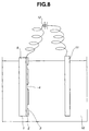
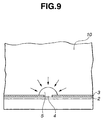
- Ni (nickel) electroplating is then performed at a bath temperature of 50 °C and a cathodic current density of 5 A/dm 2 as illustrated in Fig. 8.
- the above substrate 1 for electroplating is used as a base 9, and the electrode layer 2 is used as the cathode.
- Ni electroplating bath 10 containing nickel (II) sulfate, nickel (II) chloride, boric acid and brightener is used.
- An external electric power source 12 is connected between the electrode layer 2 and an anodic plate 11.
- Ni plated layer 5 is initially deposited in the opening 4 and grown therein.
- the plated layer 5 expands onto the mask insulating layer 3, and the semispherical microstructure 5 is thus formed as illustrated in Figs. 3D.
- the plated layer 5 is deposited until its radius reaches about 25 ⁇ m above a center of the opening 4.
- Fig. 4 shows a plan view of Fig. 3D.
- the electroplating is effected at the opening 4 in the electroplating solution 10 containing metal ions
- metal ions in the electroplating solution 10 move toward the plated layer 5, and hence, deposition of the electroplating proceeds with its growth direction being isotropic.
- a semispherical or semicylindrical plated layer can be formed.
- a microlens array has a structure of arrayed minute lenses each having a diameter from about 2 or 3 microns to about 200 or 300 microns, and the size of the opening is made smaller than the desired diameter of the microlens.
- the size of the opening is less than the diameter of the semispherical structure.
- the plated layer is formed by the deposition of metal ions in the electroplating bath caused by the electrochemical reaction.
- the thickness of the plated layer can be readily controlled by controlling the electroplating time and temperature.
- the following materials can be used as electroplating metal.
- Ni, Au, Pt, Cr, Cu, Ag, Zn and the like can be employed.
- As an alloy Cu-Zn, Sn-Co, Ni-Fe, Zn-Ni and the like can be used. Any material can be used so long as electroplating is possible.
- the first plated layer 5 can include a portion formed by electrodeposition or electroless plating.
- the surface of the first plated layer 5 only needs to be electrically conductive such that a second layer can be formed on this surface using electroplating or electrodeposition.
- the mask layer 3 is then removed by plasma ashing as illustrated in Fig. 3E.
- organic cleansing, inorganic cleansing, ultraviolet-ray ozone ashing, plasma ashing and so forth can be employed if only none of the substrate 1, electrode layer 2 and plated layer 5 are corroded thereby.
- the mask layer 3 can be removed if the mask layer 3 is not completely covered with the first plated layers 5 (see Fig. 4). Thus, the mask layer 3 can be removed without residue.
- Ni electroplating is performed at a bath temperature of 50 °C and a cathodic current density of 5 A/dm 2 .
- the same Ni electroplating bath containing nickel (II) sulfate, nickel (II) chloride, boric acid and brightener is used.
- a second plated layer 6 is thus grown until its radius reaches about 30 ⁇ m above the center of the opening 4 as illustrated in Fig. 3F. Thereby, a contact area between the semispherical plated layers 5 and 6 and the electrode layer 2 increases, and hence, the semispherical first plated layer 5 is firmly fixed to the electrode layer 2.
- the problem of deformation of the plated layers 5 and 6 due to thermal stress of the mask layer can be eliminated and a mold for forming a microstructure array with a high thermal resistivity can be obtained.
- the forming method is preferably limited to electroplating since it can take metal ions even into narrow areas, since the second plated layer 6 needs to be formed in such a narrow area between the first plated or electrodeposited layer 5 and the electrode layer 2.
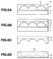
- a fabrication process for forming a microlens array by using the above structure will be described with reference to Figs. 6A to 6D.
- a resin 14 of ultraviolet-ray hardening photopolymer is deposited on the plated layers 5 and 6 as illustrated in Fig. 6A.
- the resin 14 is hardened by exposing the resin 14 to ultraviolet rays as illustrated in Fig. 6B.
- the resin 14 of a microlens array can be separated from the substrate 1 and the plated layers 5 and 6 by lifting the glass substrate 15.
- the concave resin 14 can be formed as illustrated in Fig. 6C.
- a thousand photopolymer structures 14 for the microlens array could be formed by the same microlens array mold 1, 2 and 6, using the same method. During such a process, there was no collapse of the semispherical plated layers 5 and 6.
- the resistivity of the mold is increased, and a large number of the concave resins 14 with the same profile can be fabricated using the same mold.
- the alkaline glass is not indispensable for forming a microlens, so that materials which can be used for the microlens and the substrate are less restricted than in the ion exchange method.
- the above microlens array may be fabricated by other methods, such as a method in which a conventional thermoplastic resin is used and a heated mold is stamped on this resin, a method in which a thermosetting resin is laid over a mold and then heated to be hardened, and a method in which an electron-beam hardening resin is coated on a mold and the resin is hardened by electron beam irradiation.
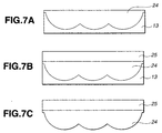
- FIG. 3A to 3F A second embodiment of a fabrication method of a semispherical microstructure array will be described by reference to Figs. 3A to 3F, 5A to 5E and 7A to 7C.
- substrate 1, electrode layer 2, insulating mask layer 3, openings 4 are formed as in the first embodiment.
- a Cu (copper) electroplating is then performed at a bath temperature of 55 °C and a cathodic current density of 4 A/dm 2 as illustrated in Fig. 8.
- the above substrate 1 for electroplating is used as a base 9, and the electrode layer 2 is used as the cathode.
- a Cu electroplating bath containing copper sulfate, sulfuric acid, chloric acid and brightener is used.
- a Cu plated layer 5 is initially deposited in the opening 4 and grown therein. The plated layer 5 expands onto the mask insulating layer 3, and the semispherical microstructure 5 is thus formed as illustrated in Figs. 3D.
- the plated layer 5 is deposited until its radius reaches about 20 ⁇ m above a center of the opening 4.
- the mask layer 3 is then removed by plasma ashing as illustrated in Fig. 3E.
- Ni electroplating is performed at a bath temperature of 50 °C and a cathodic current density of 5 A/dm 2 .
- Ni electroplating bath containing nickel (II) sulfate, nickel (II) chloride, boric acid and brightener is used.
- a second plated layer 6 is thus grown until its radius reaches about 25 ⁇ m above the center of the opening 4 as illustrated in Fig. 3F.
- a contact area between the semispherical plated layers 5 and 6 and the electrode layer 2 increases, and hence, the semispherical first plated layer 5 is firmly fixed to the electrode layer 2.
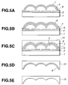
- FIG. 5A A process for fabricating a mold for forming a microlens array will be described by reference to Figs. 5A to 5E.
- the above structure is used as a master.
- PSG phospho-silicate glass
- CVD atmospheric-pressure chemical vapor deposition
- Ti and Au are continuously layered with thicknesses of 10 nm and 200 nm on the above wafer, respectively, using the electron-beam evaporation method.
- An electrode layer 8 for electroplating the mold is thus formed as illustrated in Fig. 5B.
- Ni electroplating is then performed at a bath temperature of 50 °C and a cathodic current density of 5 A/dm 2 as illustrated in Fig. 5C.
- the above master is used as a base, and the above electrode layer 8 is used as the cathode.
- Ni electroplating bath containing nickel (II) sulfate, nickel (II) chloride, boric acid and brightener is used.
- a concave mold 13 is formed as illustrated in Fig. 5C.
- the wafer of Fig. 5C is then immersed in a mixture solution of hydrofluoric acid and ammonium fluoride to etch and remove the sacrificial layer 7 of PSG.
- the substrate 1 and the mold 13 can be separated from each other as illustrated in Fig. 5D.
- the Ti of the electrode layer 8 for electroplating the mold can be removed simultaneously.
- the Au of the electrode layer 8 is etched by a mixture solution of iodine and potassium iodide.
- the mold 13 for a convex microlens array can be thus produced as illustrated in Fig. 5E.
- the separated substrate has a semispherical microstructure.
- a thousand molds 13 for a microlens array could be formed by repeating the same steps as illustrated in Figs. 5A to 5E. During such a process, there was no collapse of the semispherical plated layers. 5 and 6.
- a plurality of molds 13 with the same profile can be readily fabricated since the mold 13 is formed by molding.
- the resistivity of the mold master is increased, and a plurality of molds for a microlens array with the same profile can be fabricated using the same mold master.
- the above microlens array may also be fabricated by other methods, such as the above-described methods using thermoplastic resins, thermosetting resins and electron-beam hardening resins.
- a third embodiment of a method of fabricating a semispherical microstructure array will be described by reference to Figs. 3A to 3F, 5A to 5E and 7A to 7C.
- a silicon wafer of 1 inch in diameter is thermally oxidized using an oxidizing gas, and layers of silicon dioxide with a thickness of 1 ⁇ m are formed on opposite surfaces of the wafer.
- This wafer is used as a substrate 1 illustrated in Figs. 3A to 3F.
- Cr is layered with a thickness of 200 nm on the above wafer, using the electron beam vacuum-evaporation method.
- An electrode layer 2 of Cr is thus formed.
- Aromatic polyamide acid solution is then spin-coated and this coating is thermally treated to form a mask layer 3 of polyimide with a thickness of 1 ⁇ m as illustrated in Fig. 3A.
- photoresist are conventionally performed using photolithography to form an opening in the resist on the mask layer 3.
- the mask layer 3 at the resist opening is etched by the reactive ion etching using oxygen.
- the electrode layer 2 is partly exposed through the mask layer 3 and an opening 4 is formed as illustrated in Fig. 3B.
- the photoresist formed on the mask layer 3 is removed thereafter.
- the opening 4 has a circular shape and a diameter of 5 ⁇ m.
- a plurality of the openings 4 are formed in a two-dimensional matrix array of 500 ⁇ 500. Intervals between the adjacent openings 4 are 50 ⁇ m.
- a Cr (chromium) electroplating is then performed at a bath temperature of 45 °C and a cathodic current density of 20 A/dm 2 as illustrated in Fig. 8.
- the above substrate 1 for electroplating is used as a base 9, and the electrode layer 2 is used as the cathode.
- a Cr electroplating bath containing chromic acid and sulfuric acid is used.
- a Cr plated layer 5 is initially deposited in the opening 4 and grew therein. The plated layer 5 expands onto the mask layer 3, and the semispherical microstructure 5 is thus formed as illustrated in Figs. 3D.
- the plated layer 5 is deposited until its radius reaches about 12 ⁇ m above a center of the opening 4.
- the mask layer 3 is then removed by plasma ashing as illustrated in Fig. 3E.
- another Cr electroplating is performed at a bath temperature of 45 °C and a cathodic current density of 20 A/dm 2 .
- a Cr electroplating bath containing sulfuric acid and brightener is used.
- a second plated layer 6 is thus grown until its radius reaches about 20 ⁇ m above the center of the opening 4 as illustrated in Fig. 3F. Thereby, the semispherical first plated layer 5 is firmly fixed to the electrode layer 2.
- a mold for forming a microlens array there occur neither mold deformation nor cracks due to the molding pressure when used, and a mold master for a microlens array with excellent mechanical characteristics can be obtained.
- FIG. 5A A fabrication process for a mold will be described by reference to Figs. 5A to 5E.
- the above structure is used as a master.
- PSG of 1 ⁇ m in thickess is deposited at 350 °C by the atmospheric-pressure CVD method to form a sacrificial layer 7 as illustrated in Fig. 5A.
- Ni electroless plating is then performed at a bath temperature of 90 °C.
- Ni electroless plating bath containing nickel (II) sulfate, ethylene diamine, sodium hypophosphite and additive is used.
- a mold 13 is formed as illustrated in Fig. 5C.
- the wafer of Fig. 5C is then immersed in a mixture solution of hydrofluoric acid and ammonium fluoride to etch and remove the sacrificial layer 7 of PSG.
- the substrate 1 and the mold 13 can be separated as illustrated in Fig. 5D. Since the electroless plating is used in this embodiment, the process for forming the electrode layer 8 on the sacrificial layer 7 is unnecessary, in contrast to the second embodiment.
- the separated substrate has a semispherical microstructure.
- a thousand molds 13 for forming a microlens array could be formed by repeating the same steps as illustrated in Figs. 5A to 5E. During such a process, there was no collapse of the semispherical plated layers 5 and 6.
- a plurality of molds 13 with the same profile can be readily fabricated since the mold 13 is formed by molding.
- the resistivity of the mold master is increased, and a plurality of molds for a microlens array with the same profile can be fabricated using the same mold master.
- a substrate (1), with an electrically-conductive portion (2) is provided, an insulating mask layer (3) is formed on the electrically-conductive portion of the substrate, a plurality of openings (4) are formed in the insulating mask layer to expose the electrically-conductive portion, and a first plated or electrodeposited layer (5) is deposited in the openings and on the insulating mask layer by electro- or electroless-plating, or electrodeposition. At least a surface of the first plated or electrodeposited layer (5) is made electrically conductive.
- the insulating mask layer (3) is removed, and a second plated layer (6) is formed on the first plated or electrodeposited layer and on the electrically-conductive portion by electroplating to firmly fix the first plated or electrodeposited layer (5) to the substrate (1).
Landscapes
- Physics & Mathematics (AREA)
- Engineering & Computer Science (AREA)
- Manufacturing & Machinery (AREA)
- General Physics & Mathematics (AREA)
- Optics & Photonics (AREA)
- Microelectronics & Electronic Packaging (AREA)
- Moulds For Moulding Plastics Or The Like (AREA)
Abstract
Description
Claims (17)
- A method for fabricating an array of microstructures comprising the steps of:preparing a substrate with an electrically-conductive portion;forming an insulating mask layer on the electrically-conductive portion;forming a plurality of openings in the insulating mask layer to expose the electrically-conductive portion;forming a first plated or electrodeposited layer in the openings and on the insulating mask layer by electro- or electroless-plating, or electrodeposition, with at least a surface of the first plated or electrodeposited layer being electrically conductive;removing the insulating mask layer; andforming a second plated layer on the first plated or electrodeposited layer and on the electrically-conductive portion by electroplating.
- A fabrication method according to claim 1, wherein the step of forming the first plated or electrodeposited layer is stopped after a thickness of the first plated or electrodeposited layer reaches half a designed final height or more of the second plated layer above a central portion of the opening.
- A fabrication method according to claim 1 or 2, wherein the first plated or electrodeposited layers are formed in the step of forming the first plated or electrodeposited layer such that the insulating mask layer between the adjacent first plated or electrodeposited layers is not completely covered.
- A fabrication method according to claim 1, 2 or 3, wherein the step of forming the second plated layer is stopped after a thickness of the second plated layer reaches a thickness of the insulating mask layer or more.
- A fabrication method according to any one of claims 1 to 4, wherein the opening has a circular shape and the microstructure is a semispherical microstructure.
- A fabrication method according to any one of claims 1 to 4, wherein the opening has an elongated stripe shape and the microstructure is a semicylindrical microstructure.
- A fabrication method according to any one of claims 1 to 6, further comprising a step of forming a mold on the substrate with the first plated or electrodeposited layer and the second plated layer; and a step of separating the mold from the substrate.
- A fabrication method according to claim 7, wherein the mold is formed using electroplating.
- A fabrication method according to claim 7 or 8, wherein the mold is a mold for fabricating a microlens array.
- A fabrication method according to claim 9, further comprising a step of coating a light-transmitting material on the mold; a step of hardening the light-transmitting material; and a step of separating the material from the mold to obtain the microlens array.
- A microstructure array comprising:a substrate having an electrically-conductive portion;a first plated or electrodeposited layer formed on the electrically-conductive portion by electro- or electroless-plating or electrodeposition using a plurality of openings formed in an insulating mask layer formed on the electrically-conductive portion of the substrate to expose the electrically-conductive portion, at least a surface of the first plated or electrodeposited layer being electrically conductive, and the insulating mask layer being finally removed; anda second plated layer formed on the first plated or electrodeposited layer and on the electrically-conductive portion by electroplating.
- A microstructure array according to claim 11, wherein a height of the second plated layer formed on the first plated or electrodeposited layer above a central portion of the opening is in a range from 1 µm to 100 µm.
- A microstructure array according to claim 11 or 12, wherein a thickness of the second plated layer formed on the first plated or electrodeposited layer above a central portion of the opening is equal to or smaller than a thickness of the first plated or electrodeposited layer above the central portion of the opening.
- A microstructure array according to claim 11, 12 or 13, wherein the first plated or electrodeposited layers are formed so as not to completely cover the electrically-conductive portion.
- A microstructure array according to any one of claims 11 to 14, wherein a thickness of the second plated layer is equal to or larger than a spacing between the first plated layer and the electrically-conductive portion.
- A microstructure array according to any one of claims 11 to 15, wherein the opening has a circular shape and the microstructure is a semispherical microstructure.
- A microstructure array according to any one of claims 11 to 15, wherein the opening has an elongated stripe shape and the microstructure is a semicylindrical microstructure.
Applications Claiming Priority (2)
| Application Number | Priority Date | Filing Date | Title |
|---|---|---|---|
| JP09443699A JP3524425B2 (en) | 1999-04-01 | 1999-04-01 | Method for manufacturing mold or mold master for micro structure array, method for fabricating micro structure array manufactured using the mold or mold master |
| JP9443699 | 1999-04-01 |
Publications (2)
| Publication Number | Publication Date |
|---|---|
| EP1041406A1 true EP1041406A1 (en) | 2000-10-04 |
| EP1041406B1 EP1041406B1 (en) | 2004-10-27 |
Family
ID=14110214
Family Applications (1)
| Application Number | Title | Priority Date | Filing Date |
|---|---|---|---|
| EP20000106860 Expired - Lifetime EP1041406B1 (en) | 1999-04-01 | 2000-03-30 | Microstructure array, and methods of fabricating a microstructure array, a mold for forming a microstructure array, and a microlens array |
Country Status (5)
| Country | Link |
|---|---|
| US (2) | US6503384B1 (en) |
| EP (1) | EP1041406B1 (en) |
| JP (1) | JP3524425B2 (en) |
| KR (1) | KR100403715B1 (en) |
| DE (1) | DE60015219T2 (en) |
Cited By (1)
| Publication number | Priority date | Publication date | Assignee | Title |
|---|---|---|---|---|
| US8552473B2 (en) | 2005-09-06 | 2013-10-08 | Semiconductor Energy Laboratory Co., Ltd. | Micro-electro-mechanical device and manufacturing method for the same |
Families Citing this family (15)
| Publication number | Priority date | Publication date | Assignee | Title |
|---|---|---|---|---|
| US6788460B2 (en) * | 1998-04-15 | 2004-09-07 | Duke University | Projection screen apparatus |
| JP3524424B2 (en) * | 1999-04-01 | 2004-05-10 | キヤノン株式会社 | Mold or mold master for microstructure array, and method of manufacturing the same |
| JP3840058B2 (en) * | 2000-04-07 | 2006-11-01 | キヤノン株式会社 | Microlens, solid-state imaging device and manufacturing method thereof |
| JP2002321227A (en) * | 2001-04-25 | 2002-11-05 | Canon Inc | Method of manufacturing optical element forming mold, method of manufacturing optical element using the mold, and optical element by the manufacturing method |
| KR100490873B1 (en) * | 2001-05-17 | 2005-05-23 | 한국과학기술연구원 | Method for fabrication micro lens arrays |
| US6746823B2 (en) * | 2002-06-01 | 2004-06-08 | Industrial Technology Research Institute | Fabricating process of non-gap 3-D microstructure array mold core |
| US20040151828A1 (en) * | 2003-02-04 | 2004-08-05 | Anis Zribi | Method for fabrication and alignment of micro and nanoscale optics using surface tension gradients |
| US7227692B2 (en) * | 2003-10-09 | 2007-06-05 | Micron Technology, Inc | Method and apparatus for balancing color response of imagers |
| JP2006251691A (en) * | 2005-03-14 | 2006-09-21 | Oki Electric Ind Co Ltd | Manufacturing method of optical element |
| KR100691278B1 (en) | 2005-08-30 | 2007-03-12 | 삼성전기주식회사 | Micro lens manufacturing apparatus and micro lens manufacturing method |
| JP4379404B2 (en) * | 2005-09-28 | 2009-12-09 | 日立ライティング株式会社 | Light source module, liquid crystal display device, and light source module manufacturing method |
| KR101711646B1 (en) * | 2009-12-11 | 2017-03-03 | 엘지디스플레이 주식회사 | Mathod for forming mold for imprinting and method for forming pattern using mold for imprinting |
| JP4829360B2 (en) * | 2010-04-27 | 2011-12-07 | 株式会社東芝 | Stamper manufacturing method |
| JP2017105101A (en) | 2015-12-11 | 2017-06-15 | 株式会社ミマキエンジニアリング | Three-dimensional molded object, and three-dimensional molding apparatus and method for producing the same |
| KR102240406B1 (en) * | 2019-06-17 | 2021-04-15 | 한국기계연구원 | Micro lens array sheet, mold for fabricating the same, and method of fabricating the same |
Citations (6)
| Publication number | Priority date | Publication date | Assignee | Title |
|---|---|---|---|---|
| JPH01261601A (en) * | 1988-04-13 | 1989-10-18 | Omron Tateisi Electron Co | Nonspherical micro-lens and its manufacture and optical fiber coupler, condensing optical system, optical element, semiconductor laser light source and image device utilizing nonspherical micro-lens |
| EP0450780A2 (en) * | 1990-04-05 | 1991-10-09 | Matsushita Electric Industrial Co., Ltd. | Optical microelement array and its production method |
| JPH05303009A (en) * | 1992-04-28 | 1993-11-16 | Dainippon Printing Co Ltd | Microlens array original plate and method for producing microlens array |
| US5466926A (en) * | 1992-01-27 | 1995-11-14 | Kabushiki Kaisha Toshiba | Colored microlens array and method of manufacturing same |
| US5536455A (en) * | 1994-01-03 | 1996-07-16 | Omron Corporation | Method of manufacturing lens array |
| JPH08258051A (en) * | 1995-03-27 | 1996-10-08 | Victor Co Of Japan Ltd | Production of lens mold |
Family Cites Families (6)
| Publication number | Priority date | Publication date | Assignee | Title |
|---|---|---|---|---|
| JPS6054819A (en) * | 1983-09-05 | 1985-03-29 | Toshiba Corp | Resin molding die and manufacture thereof |
| JPS6410169A (en) | 1987-07-03 | 1989-01-13 | Kurita Water Ind Ltd | Filter device for chromatography |
| JPH0627302A (en) | 1992-07-09 | 1994-02-04 | Nitto Denko Corp | Optical element matrix and method for manufacturing the same |
| CA2084828C (en) * | 1992-12-08 | 1996-07-09 | Rene Bourque | Fastener |
| JP3015712B2 (en) * | 1995-06-30 | 2000-03-06 | 日東電工株式会社 | Film carrier and semiconductor device using the same |
| US6436265B1 (en) * | 1999-03-29 | 2002-08-20 | Canon Kabushiki Kaisha | Microstructure array, and apparatus and method for forming the microstructure array, and a mold for fabricating a microstructure array |
-
1999
- 1999-04-01 JP JP09443699A patent/JP3524425B2/en not_active Expired - Fee Related
-
2000
- 2000-03-28 US US09/536,128 patent/US6503384B1/en not_active Expired - Fee Related
- 2000-03-30 EP EP20000106860 patent/EP1041406B1/en not_active Expired - Lifetime
- 2000-03-30 DE DE60015219T patent/DE60015219T2/en not_active Expired - Lifetime
- 2000-03-31 KR KR10-2000-0016818A patent/KR100403715B1/en not_active Expired - Fee Related
-
2002
- 2002-10-04 US US10/263,745 patent/US20030024820A1/en not_active Abandoned
Patent Citations (6)
| Publication number | Priority date | Publication date | Assignee | Title |
|---|---|---|---|---|
| JPH01261601A (en) * | 1988-04-13 | 1989-10-18 | Omron Tateisi Electron Co | Nonspherical micro-lens and its manufacture and optical fiber coupler, condensing optical system, optical element, semiconductor laser light source and image device utilizing nonspherical micro-lens |
| EP0450780A2 (en) * | 1990-04-05 | 1991-10-09 | Matsushita Electric Industrial Co., Ltd. | Optical microelement array and its production method |
| US5466926A (en) * | 1992-01-27 | 1995-11-14 | Kabushiki Kaisha Toshiba | Colored microlens array and method of manufacturing same |
| JPH05303009A (en) * | 1992-04-28 | 1993-11-16 | Dainippon Printing Co Ltd | Microlens array original plate and method for producing microlens array |
| US5536455A (en) * | 1994-01-03 | 1996-07-16 | Omron Corporation | Method of manufacturing lens array |
| JPH08258051A (en) * | 1995-03-27 | 1996-10-08 | Victor Co Of Japan Ltd | Production of lens mold |
Non-Patent Citations (3)
| Title |
|---|
| PATENT ABSTRACTS OF JAPAN vol. 014, no. 015 (P - 989) 12 January 1990 (1990-01-12) * |
| PATENT ABSTRACTS OF JAPAN vol. 018, no. 106 (P - 1697) 21 February 1994 (1994-02-21) * |
| PATENT ABSTRACTS OF JAPAN vol. 1997, no. 02 28 February 1997 (1997-02-28) * |
Cited By (1)
| Publication number | Priority date | Publication date | Assignee | Title |
|---|---|---|---|---|
| US8552473B2 (en) | 2005-09-06 | 2013-10-08 | Semiconductor Energy Laboratory Co., Ltd. | Micro-electro-mechanical device and manufacturing method for the same |
Also Published As
| Publication number | Publication date |
|---|---|
| EP1041406B1 (en) | 2004-10-27 |
| US20030024820A1 (en) | 2003-02-06 |
| KR20000071528A (en) | 2000-11-25 |
| DE60015219T2 (en) | 2006-02-02 |
| JP2000280256A (en) | 2000-10-10 |
| JP3524425B2 (en) | 2004-05-10 |
| DE60015219D1 (en) | 2004-12-02 |
| US6503384B1 (en) | 2003-01-07 |
| KR100403715B1 (en) | 2003-11-01 |
Similar Documents
| Publication | Publication Date | Title |
|---|---|---|
| US6436265B1 (en) | Microstructure array, and apparatus and method for forming the microstructure array, and a mold for fabricating a microstructure array | |
| US7638027B2 (en) | Microstructure array, mold for forming a microstructure array, and method of fabricating the same | |
| US6632342B1 (en) | Methods of fabricating a microstructure array | |
| US6506623B2 (en) | Microstructure array, mold for forming a microstructure array, and method of fabricating the same | |
| US6656393B2 (en) | Mold for forming a microlens and method of fabricating the same | |
| EP1041406B1 (en) | Microstructure array, and methods of fabricating a microstructure array, a mold for forming a microstructure array, and a microlens array | |
| US6876051B2 (en) | Aspherical microstructure, and method of fabricating the same | |
| US6548144B1 (en) | Semispherical microstructure, microlens and method of fabricating the same | |
| JP3681101B2 (en) | Manufacturing method of mold master for microlens array | |
| JP3610297B2 (en) | MICROSTRUCTURE ARRAY AND METHOD FOR MANUFACTURING THE SAME | |
| JP2000271940A (en) | Microlens or microlens mold manufacturing method, microlens or microlens mold substrate used for the method | |
| JP3517640B2 (en) | Die for micro structure array, micro structure array, and method of manufacturing the same | |
| JP3513478B2 (en) | Die for micro structure array, micro structure array, and method of manufacturing the same | |
| JP2002103336A (en) | Manufacturing method of microstructure array | |
| JP2002113721A (en) | Microstructure array, mold therefor, and method for manufacturing the same |
Legal Events
| Date | Code | Title | Description |
|---|---|---|---|
| PUAI | Public reference made under article 153(3) epc to a published international application that has entered the european phase |
Free format text: ORIGINAL CODE: 0009012 |
|
| AK | Designated contracting states |
Kind code of ref document: A1 Designated state(s): CH DE FR GB IT LI |
|
| AX | Request for extension of the european patent |
Free format text: AL;LT;LV;MK;RO;SI |
|
| 17P | Request for examination filed |
Effective date: 20010214 |
|
| AKX | Designation fees paid |
Free format text: CH DE FR GB IT LI |
|
| 17Q | First examination report despatched |
Effective date: 20021030 |
|
| GRAP | Despatch of communication of intention to grant a patent |
Free format text: ORIGINAL CODE: EPIDOSNIGR1 |
|
| RIC1 | Information provided on ipc code assigned before grant |
Ipc: 7B 29D 11/00 B Ipc: 7G 02B 3/00 A |
|
| GRAS | Grant fee paid |
Free format text: ORIGINAL CODE: EPIDOSNIGR3 |
|
| GRAA | (expected) grant |
Free format text: ORIGINAL CODE: 0009210 |
|
| AK | Designated contracting states |
Kind code of ref document: B1 Designated state(s): CH DE FR GB IT LI |
|
| PG25 | Lapsed in a contracting state [announced via postgrant information from national office to epo] |
Ref country code: IT Free format text: LAPSE BECAUSE OF FAILURE TO SUBMIT A TRANSLATION OF THE DESCRIPTION OR TO PAY THE FEE WITHIN THE PRESCRIBED TIME-LIMIT;WARNING: LAPSES OF ITALIAN PATENTS WITH EFFECTIVE DATE BEFORE 2007 MAY HAVE OCCURRED AT ANY TIME BEFORE 2007. THE CORRECT EFFECTIVE DATE MAY BE DIFFERENT FROM THE ONE RECORDED. Effective date: 20041027 Ref country code: FR Free format text: LAPSE BECAUSE OF FAILURE TO SUBMIT A TRANSLATION OF THE DESCRIPTION OR TO PAY THE FEE WITHIN THE PRESCRIBED TIME-LIMIT Effective date: 20041027 Ref country code: CH Free format text: LAPSE BECAUSE OF FAILURE TO SUBMIT A TRANSLATION OF THE DESCRIPTION OR TO PAY THE FEE WITHIN THE PRESCRIBED TIME-LIMIT Effective date: 20041027 Ref country code: LI Free format text: LAPSE BECAUSE OF FAILURE TO SUBMIT A TRANSLATION OF THE DESCRIPTION OR TO PAY THE FEE WITHIN THE PRESCRIBED TIME-LIMIT Effective date: 20041027 |
|
| REG | Reference to a national code |
Ref country code: GB Ref legal event code: FG4D |
|
| REG | Reference to a national code |
Ref country code: CH Ref legal event code: EP |
|
| REF | Corresponds to: |
Ref document number: 60015219 Country of ref document: DE Date of ref document: 20041202 Kind code of ref document: P |
|
| PG25 | Lapsed in a contracting state [announced via postgrant information from national office to epo] |
Ref country code: GB Free format text: LAPSE BECAUSE OF NON-PAYMENT OF DUE FEES Effective date: 20050330 |
|
| REG | Reference to a national code |
Ref country code: CH Ref legal event code: PL |
|
| PLBE | No opposition filed within time limit |
Free format text: ORIGINAL CODE: 0009261 |
|
| STAA | Information on the status of an ep patent application or granted ep patent |
Free format text: STATUS: NO OPPOSITION FILED WITHIN TIME LIMIT |
|
| 26N | No opposition filed |
Effective date: 20050728 |
|
| GBPC | Gb: european patent ceased through non-payment of renewal fee |
Effective date: 20050330 |
|
| EN | Fr: translation not filed | ||
| PGFP | Annual fee paid to national office [announced via postgrant information from national office to epo] |
Ref country code: DE Payment date: 20100331 Year of fee payment: 11 |
|
| PG25 | Lapsed in a contracting state [announced via postgrant information from national office to epo] |
Ref country code: DE Free format text: LAPSE BECAUSE OF NON-PAYMENT OF DUE FEES Effective date: 20111001 |
|
| REG | Reference to a national code |
Ref country code: DE Ref legal event code: R119 Ref document number: 60015219 Country of ref document: DE Effective date: 20111001 |