EP1039598A2 - Distributed feedback semiconductor laser - Google Patents
Distributed feedback semiconductor laser Download PDFInfo
- Publication number
- EP1039598A2 EP1039598A2 EP00302095A EP00302095A EP1039598A2 EP 1039598 A2 EP1039598 A2 EP 1039598A2 EP 00302095 A EP00302095 A EP 00302095A EP 00302095 A EP00302095 A EP 00302095A EP 1039598 A2 EP1039598 A2 EP 1039598A2
- Authority
- EP
- European Patent Office
- Prior art keywords
- grating
- semiconductor laser
- distributed feedback
- feedback semiconductor
- laser according
- Prior art date
- Legal status (The legal status is an assumption and is not a legal conclusion. Google has not performed a legal analysis and makes no representation as to the accuracy of the status listed.)
- Withdrawn
Links
- 239000004065 semiconductor Substances 0.000 title claims abstract description 53
- 230000003287 optical effect Effects 0.000 claims abstract description 22
- 230000004888 barrier function Effects 0.000 claims abstract description 4
- 230000010363 phase shift Effects 0.000 claims description 36
- 230000010355 oscillation Effects 0.000 claims description 22
- 239000011248 coating agent Substances 0.000 claims description 7
- 238000000576 coating method Methods 0.000 claims description 7
- 238000004519 manufacturing process Methods 0.000 abstract description 6
- 230000008859 change Effects 0.000 description 8
- 230000000694 effects Effects 0.000 description 7
- 230000005284 excitation Effects 0.000 description 7
- 230000005684 electric field Effects 0.000 description 5
- 238000009826 distribution Methods 0.000 description 3
- 230000007246 mechanism Effects 0.000 description 3
- 238000000034 method Methods 0.000 description 3
- 239000000758 substrate Substances 0.000 description 3
- 238000004891 communication Methods 0.000 description 2
- 238000010586 diagram Methods 0.000 description 2
- 230000006872 improvement Effects 0.000 description 2
- 238000001228 spectrum Methods 0.000 description 2
- 230000005540 biological transmission Effects 0.000 description 1
- 230000015572 biosynthetic process Effects 0.000 description 1
- 239000000969 carrier Substances 0.000 description 1
- 230000008878 coupling Effects 0.000 description 1
- 238000010168 coupling process Methods 0.000 description 1
- 238000005859 coupling reaction Methods 0.000 description 1
- 230000007423 decrease Effects 0.000 description 1
- 230000006866 deterioration Effects 0.000 description 1
- 238000010894 electron beam technology Methods 0.000 description 1
- 238000005530 etching Methods 0.000 description 1
- 230000006698 induction Effects 0.000 description 1
- 238000001459 lithography Methods 0.000 description 1
- 239000000463 material Substances 0.000 description 1
- 239000013307 optical fiber Substances 0.000 description 1
- 230000008569 process Effects 0.000 description 1
- 238000002310 reflectometry Methods 0.000 description 1
- 230000004044 response Effects 0.000 description 1
Images




Classifications
-
- B—PERFORMING OPERATIONS; TRANSPORTING
- B82—NANOTECHNOLOGY
- B82Y—SPECIFIC USES OR APPLICATIONS OF NANOSTRUCTURES; MEASUREMENT OR ANALYSIS OF NANOSTRUCTURES; MANUFACTURE OR TREATMENT OF NANOSTRUCTURES
- B82Y20/00—Nanooptics, e.g. quantum optics or photonic crystals
-
- H—ELECTRICITY
- H01—ELECTRIC ELEMENTS
- H01S—DEVICES USING THE PROCESS OF LIGHT AMPLIFICATION BY STIMULATED EMISSION OF RADIATION [LASER] TO AMPLIFY OR GENERATE LIGHT; DEVICES USING STIMULATED EMISSION OF ELECTROMAGNETIC RADIATION IN WAVE RANGES OTHER THAN OPTICAL
- H01S5/00—Semiconductor lasers
- H01S5/10—Construction or shape of the optical resonator, e.g. extended or external cavity, coupled cavities, bent-guide, varying width, thickness or composition of the active region
- H01S5/12—Construction or shape of the optical resonator, e.g. extended or external cavity, coupled cavities, bent-guide, varying width, thickness or composition of the active region the resonator having a periodic structure, e.g. in distributed feedback [DFB] lasers
-
- H—ELECTRICITY
- H01—ELECTRIC ELEMENTS
- H01S—DEVICES USING THE PROCESS OF LIGHT AMPLIFICATION BY STIMULATED EMISSION OF RADIATION [LASER] TO AMPLIFY OR GENERATE LIGHT; DEVICES USING STIMULATED EMISSION OF ELECTROMAGNETIC RADIATION IN WAVE RANGES OTHER THAN OPTICAL
- H01S5/00—Semiconductor lasers
- H01S5/10—Construction or shape of the optical resonator, e.g. extended or external cavity, coupled cavities, bent-guide, varying width, thickness or composition of the active region
- H01S5/12—Construction or shape of the optical resonator, e.g. extended or external cavity, coupled cavities, bent-guide, varying width, thickness or composition of the active region the resonator having a periodic structure, e.g. in distributed feedback [DFB] lasers
- H01S5/1203—Construction or shape of the optical resonator, e.g. extended or external cavity, coupled cavities, bent-guide, varying width, thickness or composition of the active region the resonator having a periodic structure, e.g. in distributed feedback [DFB] lasers over only a part of the length of the active region
-
- H—ELECTRICITY
- H01—ELECTRIC ELEMENTS
- H01S—DEVICES USING THE PROCESS OF LIGHT AMPLIFICATION BY STIMULATED EMISSION OF RADIATION [LASER] TO AMPLIFY OR GENERATE LIGHT; DEVICES USING STIMULATED EMISSION OF ELECTROMAGNETIC RADIATION IN WAVE RANGES OTHER THAN OPTICAL
- H01S5/00—Semiconductor lasers
- H01S5/10—Construction or shape of the optical resonator, e.g. extended or external cavity, coupled cavities, bent-guide, varying width, thickness or composition of the active region
- H01S5/12—Construction or shape of the optical resonator, e.g. extended or external cavity, coupled cavities, bent-guide, varying width, thickness or composition of the active region the resonator having a periodic structure, e.g. in distributed feedback [DFB] lasers
- H01S5/124—Construction or shape of the optical resonator, e.g. extended or external cavity, coupled cavities, bent-guide, varying width, thickness or composition of the active region the resonator having a periodic structure, e.g. in distributed feedback [DFB] lasers incorporating phase shifts
- H01S5/1243—Construction or shape of the optical resonator, e.g. extended or external cavity, coupled cavities, bent-guide, varying width, thickness or composition of the active region the resonator having a periodic structure, e.g. in distributed feedback [DFB] lasers incorporating phase shifts by other means than a jump in the grating period, e.g. bent waveguides
-
- H—ELECTRICITY
- H01—ELECTRIC ELEMENTS
- H01S—DEVICES USING THE PROCESS OF LIGHT AMPLIFICATION BY STIMULATED EMISSION OF RADIATION [LASER] TO AMPLIFY OR GENERATE LIGHT; DEVICES USING STIMULATED EMISSION OF ELECTROMAGNETIC RADIATION IN WAVE RANGES OTHER THAN OPTICAL
- H01S5/00—Semiconductor lasers
- H01S5/10—Construction or shape of the optical resonator, e.g. extended or external cavity, coupled cavities, bent-guide, varying width, thickness or composition of the active region
- H01S5/12—Construction or shape of the optical resonator, e.g. extended or external cavity, coupled cavities, bent-guide, varying width, thickness or composition of the active region the resonator having a periodic structure, e.g. in distributed feedback [DFB] lasers
- H01S5/124—Construction or shape of the optical resonator, e.g. extended or external cavity, coupled cavities, bent-guide, varying width, thickness or composition of the active region the resonator having a periodic structure, e.g. in distributed feedback [DFB] lasers incorporating phase shifts
- H01S5/1246—Construction or shape of the optical resonator, e.g. extended or external cavity, coupled cavities, bent-guide, varying width, thickness or composition of the active region the resonator having a periodic structure, e.g. in distributed feedback [DFB] lasers incorporating phase shifts plurality of phase shifts
-
- H—ELECTRICITY
- H01—ELECTRIC ELEMENTS
- H01S—DEVICES USING THE PROCESS OF LIGHT AMPLIFICATION BY STIMULATED EMISSION OF RADIATION [LASER] TO AMPLIFY OR GENERATE LIGHT; DEVICES USING STIMULATED EMISSION OF ELECTROMAGNETIC RADIATION IN WAVE RANGES OTHER THAN OPTICAL
- H01S5/00—Semiconductor lasers
- H01S5/30—Structure or shape of the active region; Materials used for the active region
- H01S5/34—Structure or shape of the active region; Materials used for the active region comprising quantum well or superlattice structures, e.g. single quantum well [SQW] lasers, multiple quantum well [MQW] lasers or graded index separate confinement heterostructure [GRINSCH] lasers
- H01S5/3403—Structure or shape of the active region; Materials used for the active region comprising quantum well or superlattice structures, e.g. single quantum well [SQW] lasers, multiple quantum well [MQW] lasers or graded index separate confinement heterostructure [GRINSCH] lasers having a strained layer structure in which the strain performs a special function, e.g. general strain effects, strain versus polarisation
Definitions
- the present invention relates to a semiconductor laser and more particularly to a distributed feedback semiconductor laser with strong capacity to tolerate return light which is utilized as an integrated light source.
- the semiconductor laser is, at present, widely used as a light source for a high-volume long-distance optical fiber communication.
- the conventional semiconductor laser has a problem that a very small amount of return light reflected back from optical components such as optical connectors may induce noises in the inside of the semiconductor laser and cause code errors in transmission.
- the optical isolator used to remove such return light from the semiconductor laser has drawbacks of requiring a large number of manufacturing steps to work materials and make assembly in fabrication thereof and, thus, of costing a great deal. Accordingly, there has been sought a new development of a semiconductor laser with strong capacity to tolerate return light, possible to be used without an optical isolator, in other words, a semiconductor laser having an excellent resistance against return light (hard to be affected by return light).
- DFB laser distributed feedback semiconductor laser
- Fig. 8 shows an active layer 83 of a known DFB laser
- an excitation region a region into which a current is introduced
- a non-excitation region is utilized as a distributed reflector.
- return light can be inhibited from entering the excitation region of the active layer, even if the edge face is not coated with a multi-layered dielectric film.
- a distributed feedback semiconductor laser whose optical feedback is provided at least by a diffraction grating;
- a distributed feedback semiconductor laser having a tensile strain quantum well active layer in accordance with the present invention has a small linewidth enhancement factor for the active layer so that a change in refractive index of the inside of the semiconductor laser cavity which may be caused by return light reflected back from the outside or the direct modulation can be well controlled and, thus, fluctuations of the optical output and the oscillation wavelength can be inhibited. Consequently, a semiconductor laser with an excellent resistance against return light as well as a low chirping has become obtainable. Furthermore, a semiconductor laser of the present invention can produce the above effects without damaging its intrinsic laser characteristics, and besides a simple structure it possesses ensures an easy process for manufacturing.
- Fig. 1 is a diagram illustrating a generation mechanism of optical output fluctuations in a DFB laser which are induced by return light.
- the electric field E and the carrier density N within the laser are varied and this leads to a change in an equivalent refractive index n eq .
- oscillation conditions of the DFB laser namely the mirror loss ⁇ m (relating to the oscillation threshold) as well as the amount of detuning ⁇ ß (relating to the oscillation wavelength) are altered so that the optical output and the oscillation wavelength ⁇ are changed.
- ⁇ ß 2 n eq ⁇ ( 1 / ⁇ - 1 / ⁇ B ) , where ⁇ B is the Bragg wavelength.
- Fig. 2 shows calculated results of optical output variations of the DFB laser at the time of digital modulation, with the return light at 0, - 20 dB and -30 dB, respectively, which were obtained through the large signal analysis.
- Fig. 2 indicates that, when return light enters, with vacillation of the optical output taking place, a fluctuation component such as shown in the drawing is added to a Hi level of the response waveform. Such output fluctuations may pass through a filter and lead to an outbreak of responsivity penalties in a communication system.
- a control over a change in an equivalent refractive index can inhibit oscillation conditions of the DFB laser from changing and, therefore, can reduce fluctuations of the optical output as well as the oscillation wavelength.
- a tensile strain multiple quantum well (a tensile strain MQW)
- a light whole band is raised to become a first level of a valance band thereof, owing to the effect of tensile strain.
- a high differential gain g and a low linewidth enhancement factor ⁇ can be obtained.
- TM tensile strain single quantum well
- TE compressive strain single quantum well
- TE non-strain single quantum well
- dg/dN of the tensile strain quantum well is considerably large, compared with those of the compressive strain quantum well and non-strain quantum well.
- Table 1 summarizes the free carrier plasma effect on the linewidth enhancement factor ⁇ .
- L W in the Table represents the thickness of the quantum well.
- a change in refractive index due to change of carrier density is small. Because of this, oscillation conditions of the laser can be inhibited from changing and, therefore, fluctuations of the optical output as well the oscillation wavelength can be reduced. Accordingly, in the present system, through the use of a structure in which a tensile strain quantum well with a small linewidth enhancement factor is employed for the active layer, an improvement in the resistance against return light of the DFB laser is achieved.
- an application of a modulation signal to the DFB laser forces to change the carrier density within laser cavity. This leads to a change in the refractive index and, consequently, to shifts of the oscillation wavelength.
- the active layer in structure utilizes a tensile strain quantum well with a small linewidth enhancement factor, a change in the refractive index is controlled and fluctuations of the oscillation wavelength, reduced and, therefore, a DFB laser with a low chirping can be acquired.
- Fig. 4 is a schematic view showing a structure of a semiconductor laser that is a first embodiment of the present invention.
- a semiconductor laser of the present embodiment has a cavity length of 250 ⁇ m and a grating 2 thereof is formed on an InP semiconductor substrate 1 by a known method of electron beam exposure and lithography.
- a grating 2 thereof is formed on an InP semiconductor substrate 1 by a known method of electron beam exposure and lithography.
- an InGaAsP optical waveguide layer 3 (0.1 ⁇ m in thickness)
- a triple-layered tensile strain multiple quantum well active layer 4 well layers : three 12 nm-thick layers; barrier layers : two 15 nm-thick layers
- an InGaAsP clad layer 5 3 ⁇ m in thickness
- an InP cap layer 6 0.2 ⁇ m in thickness
- electrodes 7 and 8 are formed on the side of the InP cap layer 6 and on the side of the InP semiconductor substrate 1, respectively. Further, an anti-reflection (AR) coating film 9 and a high-reflection (HR) coating film 10 are applied to a front edge face of the semiconductor laser and to a rear edge face, respectively.
- AR anti-reflection
- HR high-reflection
- the magnitude of the tensile strain of the quantum well is set to be not less than - 0.5 % in order to make the linewidth enhancement factor of the well layer 3 or less.
- the depth of etching for fabrication of said grating 2 is set to be 0. 03 ⁇ m so as to set the DFB coupling constant ⁇ to be approximately 70 / cm.
- the grating period ⁇ herein is 202.7 nm.
- a well layer constituting a quantum well structure is preferably a tensile strain quantum well layer whose linewidth enhancement factor ⁇ at the gain peak wavelength is not greater than 3 and more preferably one with a linewidth enhancement factor ⁇ of 0 to 3.
- the active layer of the DFB laser of the present embodiment utilizes a tensile strain quantum well with a small linewidth enhancement factor, in this manner, fluctuations of the optical output caused by return light can be inhibited. Consequently, the resistance against return light can be enhanced. Furthermore, shifts of the oscillation wavelength resulting from the direct modulation can be controlled and, therefore, a DFB laser with a low chirping can be accomplished.
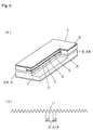
- Fig. 5 (a) is a schematic view showing a structure of a semiconductor laser that is a second embodiment of the present invention.
- a semiconductor laser of the present embodiment has the same structure as the first embodiment except that a grating 2 with a phase shift section 11 shown in Fig. 5 (b) is formed on an InP semiconductor substrate 1 and that anti-reflection (AR) coating films 9 are applied to both edge faces.
- a grating 2 with a phase shift section 11 shown in Fig. 5 (b) is formed on an InP semiconductor substrate 1 and that anti-reflection (AR) coating films 9 are applied to both edge faces.
- the grating is divided into two regions and a phase shift section 11 is interposed between these two regions.
- the amount of the phase shift is set to be ⁇ /4, corresponding to ⁇ /8.
- the amount of this phase shift preferably corresponds to ⁇ /5 - ⁇ /8.
- the active layer of the DFB laser of the present embodiment utilizes a tensile strain quantum well with a small linewidth enhancement factor and besides the phase shift section 11 with the amount of phase shifts corresponding to ⁇ /8 is incorporated thereinto, in this manner, fluctuations of the optical output caused by return light can be inhibited. Consequently, the resistance against return light can be enhanced. Furthermore, shifts of the oscillation wavelength resulting from the direct modulation can be controlled and, therefore, a DFB laser with a low chirping can be accomplished.
- Fig. 6 is a schematic view showing a structure of a semiconductor laser that is a third embodiment of the present invention.
- a semiconductor laser of the present embodiment has the same structure as the first embodiment except that a grating 2 is formed only partially along the direction of the cavity length and this grating formation region is specifically located on the side of the front edge face of the cavity and that an AR coating film is formed on a front edge face while a HR coating film is formed on a rear edge face.
- the active layer of the DFB laser of the present embodiment utilizes a tensile strain quantum well with a small linewidth enhancement factor and besides a grating is set partially therein, in this manner, fluctuations of the optical output and the oscillation wavelength caused by return light and the direct modulation can be inhibited. Further, due to the presence of the edge face phase, the resistance against return light can be enhanced and the variations of chirping characteristics can be controlled.
- Fig. 7(a) is a schematic view showing a structure of a grating of a semiconductor laser that is a fourth embodiment of the present invention.
- a semiconductor laser of the fourth embodiment has the same structure as the first embodiment except that a grating thereof has a different structure.
- a grating of the fourth embodiment has a structure in which a phase shift section 11 is located not at the center of the laser cavity but a position 1/4 of the cavity length distant from the front edge face. While it is set for the present embodiment that the amount of the phase shift corresponds to ⁇ /8, it preferably corresponds to ⁇ /5 - ⁇ /8.
- phase shift region is located around the front edge face (the face for laser emission) so that the field intensity around the front edge face becomes large, which enhances the resistance against return light and reduces chirping and, at the same time, improves the output efficiency of the laser.
- Figs. 7(b) - (d) are schematic views showing respective structures of gratings of semiconductor lasers that are fifth to seventh embodiments of the present invention.
- Semiconductor lasers of the fifth to seventh embodiments have the same structure as the first embodiment except that gratings thereof have different structures.
- a grating of the fifth embodiment has a structure in which the grating is divided into a plurality of regions and a phase shift section is interposed in every interval between said regions, and the sum of the amounts of the phase shifts of these phase shift sections, that is, the total amount of the phase shifts corresponds to ⁇ /8.
- the amount of the phase shifts, in total preferably corresponds to ⁇ /5 - ⁇ /8. In case the total amount of phase shifts is in this range, a laser with better resistance against return light can be attained.
- a grating of the sixth embodiment has a structure in which grating periods gradually increases from the center of the laser cavity towards one direction (right direction) and gradually decreases towards the other direction (left direction), with the rates of changes in both directions having the same absolute value but the reversed sign to each other.
- the amount of phase shifts with respect to the average grating period over the whole cavity corresponds to ⁇ /8.
- the amount of phase shifts preferably corresponds to ⁇ /5 - ⁇ /8. In case the total amount of phase shifts, as a whole, is in this range, a laser with better resistance against return light can be attained.
- a grating of the seventh embodiment has a structure in which a laser cavity is divided into a plurality of regions along the direction of the cavity length and the grating period, at least, in one of these regions is different from the rest.
- the cavity is divided into three regions and the gratings in the first and the third regions have the same period ⁇ 1, while the grating in the second region has a different period ⁇ 2.
- the amount of the phase shifts over the whole grating corresponds to ⁇ /8.
- the amount of the phase shifts over the whole grating preferably corresponds to ⁇ /5 - ⁇ /8. In case the amount of phase shifts as a whole is in this range, a laser with better resistance against return light can be attained.
- phase-shifted DFB lasers In known phase-shifted DFB lasers, the distribution of the electric field is non-uniform, with the electric field being high in the central section (or in the phase-shift regions) and spatial hole burning is liable to happen.
- structures of the fifth to seventh embodiments can provide improvements in the uniformity of the field distribution in the inside of the laser cavity. Further, since the amount of the phase shifts in total is set to correspond to ⁇ /m, the fluctuations of the optical output and the oscillation wavelength caused by return light and the direct modulation can be further inhibited and a DFB laser having good resistance against return light and low chirping can be attained.
Landscapes
- Physics & Mathematics (AREA)
- Optics & Photonics (AREA)
- Condensed Matter Physics & Semiconductors (AREA)
- General Physics & Mathematics (AREA)
- Electromagnetism (AREA)
- Chemical & Material Sciences (AREA)
- Engineering & Computer Science (AREA)
- Nanotechnology (AREA)
- Life Sciences & Earth Sciences (AREA)
- Biophysics (AREA)
- Crystallography & Structural Chemistry (AREA)
- Semiconductor Lasers (AREA)
Abstract
Description

Claims (9)
- A distributed feedback semiconductor laser whose optical feedback is provided at least by a diffraction grating; whereinan active layer has a quantum well structure comprising a well layer and a barrier layer; andsaid well layer is made of a tensile strain quantum well layer.
- The distributed feedback semiconductor laser according to Claim 1, wherein a linewidth enhancement factor at the gain peak for said well layer is not greater than 3.
- The distributed feedback semiconductor laser according to Claim 1; whereinsaid grating is formed only partially along the direction of the cavity length; andthe region with said grating being formed is specifically located on the side of one edge face, while a high reflection coating film is applied onto the other edge face on the side where no grating is formed.
- The distributed feedback semiconductor laser according to Claim 1; whereina grating contained within the laser cavity is divided into M regions (M is an integer satisfying M>2) along the direction of the cavity length, and a phase shift section is interposed in every interval between said regions; andthe total amount of phase shifts of said phase shift sections corresponds to λ/m (λ is the oscillation wavelength and m is a positive real number).
- The distributed feedback semiconductor laser according to Claim 4; whereinsaid phase shift sections are specifically located on the side of the edge face for laser emission.
- The distributed feedback semiconductor laser according to Claim 4 or 5; wherein the total amount of said phase shifts corresponds to λ/5 -λ/8.
- The distributed feedback semiconductor laser according to Claim 1; whereinsaid grating is formed in such a manner as the grating period gradually changes from the center of the laser cavity towards both edge faces, with the rates of changes in both directions having the same absolute value but the reversed sign to each other.
- The distributed feedback semiconductor laser according to Claim 1; whereina grating contained within the laser cavity is divided into a plurality of regions along the direction of the cavity length, and the grating period, at least, in one of these regions is different from the rest; andthe amount of phase shifts over the whole grating corresponds to λ/m (λ is the oscillation wavelength and m is a positive real number).
- The distributed feedback semiconductor laser according to Claim 7 or 8; wherein the amount of said phase shifts over the whole grating corresponds to λ/5 -λ/8.
Applications Claiming Priority (2)
| Application Number | Priority Date | Filing Date | Title |
|---|---|---|---|
| JP11079978A JP2000277851A (en) | 1999-03-24 | 1999-03-24 | Distributed feedback semiconductor laser |
| JP7997899 | 1999-03-24 |
Publications (2)
| Publication Number | Publication Date |
|---|---|
| EP1039598A2 true EP1039598A2 (en) | 2000-09-27 |
| EP1039598A3 EP1039598A3 (en) | 2004-01-21 |
Family
ID=13705426
Family Applications (1)
| Application Number | Title | Priority Date | Filing Date |
|---|---|---|---|
| EP00302095A Withdrawn EP1039598A3 (en) | 1999-03-24 | 2000-03-15 | Distributed feedback semiconductor laser |
Country Status (2)
| Country | Link |
|---|---|
| EP (1) | EP1039598A3 (en) |
| JP (1) | JP2000277851A (en) |
Families Citing this family (8)
| Publication number | Priority date | Publication date | Assignee | Title |
|---|---|---|---|---|
| JP2003204114A (en) | 2002-01-07 | 2003-07-18 | Nec Corp | Distributed feedback semiconductor laser and its manufacturing method |
| JP4735574B2 (en) * | 2006-03-24 | 2011-07-27 | 三菱電機株式会社 | Semiconductor laser and semiconductor laser module |
| JP5119789B2 (en) * | 2007-08-01 | 2013-01-16 | 富士通株式会社 | Quantum dot semiconductor laser |
| JP2010278395A (en) * | 2009-06-01 | 2010-12-09 | Nippon Telegr & Teleph Corp <Ntt> | Direct modulation semiconductor laser |
| JP6355888B2 (en) * | 2013-01-31 | 2018-07-11 | 日本オクラロ株式会社 | Semiconductor laser device and optical semiconductor device |
| JP2017216353A (en) * | 2016-05-31 | 2017-12-07 | 日本電信電話株式会社 | Distributed feedback laser |
| JP2017152724A (en) * | 2017-04-24 | 2017-08-31 | 日本オクラロ株式会社 | Semiconductor laser device and optical semiconductor device |
| JP2019160842A (en) * | 2018-03-07 | 2019-09-19 | 富士通株式会社 | Semiconductor laser and optical communication device |
Family Cites Families (4)
| Publication number | Priority date | Publication date | Assignee | Title |
|---|---|---|---|---|
| JPS62219684A (en) * | 1986-03-20 | 1987-09-26 | Fujitsu Ltd | Distributed feedback type semiconductor laser |
| JPH05145184A (en) * | 1991-11-20 | 1993-06-11 | Toshiba Corp | Wavelength variable distribution feedback type semiconductor laser and its driving method |
| US5784399A (en) * | 1996-12-19 | 1998-07-21 | Xerox Corporation | Polarization mode selection by distributed Bragg reflector in a quantum well laser |
| JP3180725B2 (en) * | 1997-08-05 | 2001-06-25 | 日本電気株式会社 | Distributed feedback semiconductor laser |
-
1999
- 1999-03-24 JP JP11079978A patent/JP2000277851A/en active Pending
-
2000
- 2000-03-15 EP EP00302095A patent/EP1039598A3/en not_active Withdrawn
Also Published As
| Publication number | Publication date |
|---|---|
| JP2000277851A (en) | 2000-10-06 |
| EP1039598A3 (en) | 2004-01-21 |
Similar Documents
| Publication | Publication Date | Title |
|---|---|---|
| US8477819B2 (en) | Semiconductor laser diode device and method of fabrication thereof | |
| US6577660B1 (en) | Distributed feedback type semiconductor laser device having gradually-changed coupling coefficient | |
| EP0978911A2 (en) | Optical functional devices, their manufacturing method and optical communication system | |
| US5272714A (en) | Distributed phase shift semiconductor laser | |
| JP3180725B2 (en) | Distributed feedback semiconductor laser | |
| US6330268B1 (en) | Distributed feedback semiconductor laser | |
| US20020181529A1 (en) | Single-transverse-mode laser diode with multi-mode waveguide region and manufacturing method of the same | |
| CA2068443C (en) | Gain-coupled distributed-feedback semiconductor laser | |
| US20020037024A1 (en) | Distributed feedback semiconductor laser | |
| EP1039598A2 (en) | Distributed feedback semiconductor laser | |
| US6825505B2 (en) | Phase-shifted distributed feedback type semiconductor laser diode capable of improving wavelength chirping and external reflection return light characteristics | |
| EP0285104B1 (en) | Distributed feedback semiconductor laser | |
| EP0727852B1 (en) | DFB laser with loss coupling and its use | |
| WO2005011076A1 (en) | Weakly guiding ridge waveguides with vertical gratings | |
| US6084901A (en) | Semiconductor laser device | |
| EP1037343A2 (en) | Distributed feedback semiconductor laser | |
| US5469459A (en) | Laser diode element with excellent intermodulation distortion characteristic | |
| US6574261B2 (en) | Distributed feedback semiconductor laser | |
| US6608850B1 (en) | Semiconductor laser apparatus | |
| JP3595677B2 (en) | Optical isolator, distributed feedback laser and optical integrated device | |
| JP3261679B2 (en) | Driving method of distributed feedback semiconductor laser | |
| JP2003152272A (en) | Dispersed phase shift structure distributed feedback semiconductor laser | |
| JP7827214B2 (en) | Semiconductor laser, method for designing diffraction grating layer of semiconductor laser, and method for manufacturing semiconductor laser | |
| KR100405940B1 (en) | Laterally coupled cavity laser diode | |
| Kitamura et al. | High performance and highly reliable lambda/4 shifted MQW-DFB-DC-PBH-LDs for Gb/s coherent optical communication systems |
Legal Events
| Date | Code | Title | Description |
|---|---|---|---|
| PUAI | Public reference made under article 153(3) epc to a published international application that has entered the european phase |
Free format text: ORIGINAL CODE: 0009012 |
|
| AK | Designated contracting states |
Kind code of ref document: A2 Designated state(s): AT BE CH CY DE DK ES FI FR GB GR IE IT LI LU MC NL PT SE |
|
| AX | Request for extension of the european patent |
Free format text: AL;LT;LV;MK;RO;SI |
|
| PUAL | Search report despatched |
Free format text: ORIGINAL CODE: 0009013 |
|
| AK | Designated contracting states |
Kind code of ref document: A3 Designated state(s): AT BE CH CY DE DK ES FI FR GB GR IE IT LI LU MC NL PT SE |
|
| AX | Request for extension of the european patent |
Extension state: AL LT LV MK RO SI |
|
| 17P | Request for examination filed |
Effective date: 20040112 |
|
| 17Q | First examination report despatched |
Effective date: 20040405 |
|
| AKX | Designation fees paid |
Designated state(s): FR GB |
|
| REG | Reference to a national code |
Ref country code: DE Ref legal event code: 8566 |
|
| STAA | Information on the status of an ep patent application or granted ep patent |
Free format text: STATUS: THE APPLICATION IS DEEMED TO BE WITHDRAWN |
|
| 18D | Application deemed to be withdrawn |
Effective date: 20040817 |