EP1039470A2 - Semiconductor memory device - Google Patents
Semiconductor memory device Download PDFInfo
- Publication number
- EP1039470A2 EP1039470A2 EP00106347A EP00106347A EP1039470A2 EP 1039470 A2 EP1039470 A2 EP 1039470A2 EP 00106347 A EP00106347 A EP 00106347A EP 00106347 A EP00106347 A EP 00106347A EP 1039470 A2 EP1039470 A2 EP 1039470A2
- Authority
- EP
- European Patent Office
- Prior art keywords
- transistor
- line
- memory cell
- bit line
- sense amplifier
- Prior art date
- Legal status (The legal status is an assumption and is not a legal conclusion. Google has not performed a legal analysis and makes no representation as to the accuracy of the status listed.)
- Withdrawn
Links
Images








Classifications
-
- G—PHYSICS
- G11—INFORMATION STORAGE
- G11C—STATIC STORES
- G11C7/00—Arrangements for writing information into, or reading information out from, a digital store
- G11C7/06—Sense amplifiers; Associated circuits, e.g. timing or triggering circuits
-
- G—PHYSICS
- G11—INFORMATION STORAGE
- G11C—STATIC STORES
- G11C11/00—Digital stores characterised by the use of particular electric or magnetic storage elements; Storage elements therefor
- G11C11/21—Digital stores characterised by the use of particular electric or magnetic storage elements; Storage elements therefor using electric elements
- G11C11/34—Digital stores characterised by the use of particular electric or magnetic storage elements; Storage elements therefor using electric elements using semiconductor devices
- G11C11/40—Digital stores characterised by the use of particular electric or magnetic storage elements; Storage elements therefor using electric elements using semiconductor devices using transistors
- G11C11/401—Digital stores characterised by the use of particular electric or magnetic storage elements; Storage elements therefor using electric elements using semiconductor devices using transistors forming cells needing refreshing or charge regeneration, i.e. dynamic cells
- G11C11/4063—Auxiliary circuits, e.g. for addressing, decoding, driving, writing, sensing or timing
- G11C11/407—Auxiliary circuits, e.g. for addressing, decoding, driving, writing, sensing or timing for memory cells of the field-effect type
- G11C11/409—Read-write [R-W] circuits
- G11C11/4091—Sense or sense/refresh amplifiers, or associated sense circuitry, e.g. for coupled bit-line precharging, equalising or isolating
-
- G—PHYSICS
- G11—INFORMATION STORAGE
- G11C—STATIC STORES
- G11C11/00—Digital stores characterised by the use of particular electric or magnetic storage elements; Storage elements therefor
- G11C11/21—Digital stores characterised by the use of particular electric or magnetic storage elements; Storage elements therefor using electric elements
- G11C11/34—Digital stores characterised by the use of particular electric or magnetic storage elements; Storage elements therefor using electric elements using semiconductor devices
- G11C11/40—Digital stores characterised by the use of particular electric or magnetic storage elements; Storage elements therefor using electric elements using semiconductor devices using transistors
- G11C11/401—Digital stores characterised by the use of particular electric or magnetic storage elements; Storage elements therefor using electric elements using semiconductor devices using transistors forming cells needing refreshing or charge regeneration, i.e. dynamic cells
- G11C11/4063—Auxiliary circuits, e.g. for addressing, decoding, driving, writing, sensing or timing
- G11C11/407—Auxiliary circuits, e.g. for addressing, decoding, driving, writing, sensing or timing for memory cells of the field-effect type
- G11C11/408—Address circuits
- G11C11/4085—Word line control circuits, e.g. word line drivers, - boosters, - pull-up, - pull-down, - precharge
-
- G—PHYSICS
- G11—INFORMATION STORAGE
- G11C—STATIC STORES
- G11C5/00—Details of stores covered by group G11C11/00
- G11C5/06—Arrangements for interconnecting storage elements electrically, e.g. by wiring
- G11C5/063—Voltage and signal distribution in integrated semi-conductor memory access lines, e.g. word-line, bit-line, cross-over resistance, propagation delay
-
- G—PHYSICS
- G11—INFORMATION STORAGE
- G11C—STATIC STORES
- G11C8/00—Arrangements for selecting an address in a digital store
- G11C8/08—Word line control circuits, e.g. drivers, boosters, pull-up circuits, pull-down circuits, precharging circuits, for word lines
-
- G—PHYSICS
- G11—INFORMATION STORAGE
- G11C—STATIC STORES
- G11C7/00—Arrangements for writing information into, or reading information out from, a digital store
- G11C7/18—Bit line organisation; Bit line lay-out
-
- G—PHYSICS
- G11—INFORMATION STORAGE
- G11C—STATIC STORES
- G11C8/00—Arrangements for selecting an address in a digital store
- G11C8/14—Word line organisation; Word line lay-out
Definitions
- the present invention relates to a semiconductor memory device such as a dynamic RAM (Random Access Memory) suitable for integration on a semiconductor substrate together with a logic circuit.
- a semiconductor memory device such as a dynamic RAM (Random Access Memory) suitable for integration on a semiconductor substrate together with a logic circuit.
- DRAM dynamic RAMs
- ASIC application specific integrated circuits
- Figs. 1A to 3B schematically show a fabrication process of a conventional semiconductor memory device having a DRAM formed of two metal interconnection layers and a logic circuit utilizing this DRAM embedded on the same semiconductor substrate.
- Figs. 1A-3A correspond to the partial sectional views of the DRAM region whereas Figs. 1B-3B correspond to the partial cross sectional views of the logic circuit region.
- a field oxide film 2 for element isolation on an Si (silicon) substrate 1 As shown in Figs. 1A and 1B, following the formation of a field oxide film 2 for element isolation on an Si (silicon) substrate 1, a gate oxide film 3, a gate electrode 4 of a transistor of polycrystalline silicon, a word line (gate line) 4a, a silicon oxide film 5 thereon, and diffusion layers 6 and 6a are formed.
- An interlayer insulation film 217 is formed thereon by CVD. Then, an opening is formed at a portion of interlayer insulation film 217 for capacitor formation by a photoresist process and dry etching process.
- the process of thin film deposition, photoresist and dry etching is repeated to sequentially form a storage electrode 201 of the memory cell capacitor shown in Fig. 2A, a capacitor insulating film 202, and a cell plate electrode 203. Then, an interlayer insulating film 204 is formed thereon including the logic circuit region.
- the above wiring and interlayer insulating film are deposited alternately and processed to form a bit line 206 constituted by a polycrystalline silicon film and a tungsten polycide film, and a contact hole 205 connecting bit line 206 with diffusion layer 6a. Then, an interlayer insulating film 207 is formed thereon including the logic circuit region.
- a memory cell is formed of a memory cell transistor for address selection and a memory cell capacitor for data storage.
- the data storage operation is effected by storing charge in the memory cell capacitor. The amount of stored charge must be increased in order to read out data properly and speedily, and in order to lengthen the data retaining time.
- the amount of charge stored in the memory cell capacitor of a DRAM is proportional to the voltage written into the memory cell.
- the write voltage of H (logical high) data is represented as below.
- the write voltage can be increased by minimizing the second term (Vtn + ⁇ ) of equation 1 ⁇
- the voltage of the word line is set higher than power supply voltage Vcc to cancel the minus of the second term.
- Japanese Patent Laying-Open No. 10-134570 discloses the usage of a transistor having a threshold value lower than that of the general one (approximately 0.6 V) for the memory cell. Accordingly, the second term of the aforementioned equation 1 ⁇ can be reduced.
- the so-called shared sense amplifier system is employed.
- the sense amplifier is connected via the switching transistors disposed at both sides to the bit line pair arranged at both sides of the switching transistors. Accordingly, a write voltage is applied to the memory cell capacitor through a switching transistor and a memory cell transistor.
- the voltage applied to the memory cell capacitor depends upon the threshold values of both the switching transistor and the memory cell transistor, and will be reduced by the threshold value of either of the two transistors that has the greater threshold value.
- the threshold value of the switching transistor must also be of a similar low level.
- An object of the present invention is to provide a semiconductor memory device that has the write voltage of a memory cell capacitor increased.
- a semiconductor memory device includes a first switching transistor for connecting a bit line extending from a memory sub array having a memory cell transistor to a first sense amplifier.
- the first switching transistor is arranged at a side opposite to the memory sub array than the input side of the sense amplifier.
- the first sense amplifier includes a first P channel sense amplifier and an N channel sense amplifier
- the first switching transistor is arranged between the first P channel sense amplifier and N channel sense amplifier to effect isolation and connection therebetween.
- a semiconductor memory device includes a first common bit line, a second common bit line, an N channel sense amplifier, a first bit line, a second bit line, a first P channel sense amplifier, a first switching transistor, a second switching transistor, a third bit line, a fourth bit line, a second P channel sense amplifier, a third switching transistor, a fourth switching transistor, a word line, a memory cell capacitor, and a memory cell transistor.
- the second common bit line is complementary to the first common bit line.
- the N channel sense amplifier is connected between the first and second common bit lines.
- the second bit line is complementary to the first bit line.
- the first P channel sense amplifier is connected between the first and second bit lines.
- the first switching transistor is connected between the first common bit line and the first bit line.
- the second switching transistor is connected between the second common bit line and the second bit line.
- the fourth bit line is complementary to the third bit line.
- the second P channel sense amplifier is connected between the third and fourth bit lines.
- the third switching transistor is connected between the first common bit line and the third bit line.
- the fourth switching transistor is connected between the second common bit line and the fourth bit line.
- the memory cell transistor has a gate connected between the first bit line and the memory cell capacitor, and connected to a word line.
- the first P channel sense amplifier amplifies directly the voltage of the first or second bit line to the power supply voltage without the involvement of the first or second switching transistor. Therefore, the write voltage of the memory cell capacitor is increased to allow a larger storage capacity for the memory cell.
- the memory cell transistor has a threshold value lower than the threshold value of the first switching transistor. Accordingly, the storage capacity of the memory cell is further increased.
- the semiconductor memory device further includes an N channel drive transistor connected between a power supply node and the first P channel sense amplifier.
- the first P channel sense amplifier can apply a voltage lower than the power supply voltage by the threshold voltage of the N channel drive transistor to the first or second bit line.
- a semiconductor memory device includes a semiconductor substrate, a dynamic random access memory formed on the semiconductor substrate, and a logic circuit formed on the semiconductor substrate to control the dynamic random access memory.
- a memory cell capacitor in the dynamic random access memory includes a capacitor insulating film of a thickness substantially identical to that of the gate insulating film of the transistor that forms the logic circuit. Accordingly, the capacitor insulating film of the memory cell capacitor can be formed in a step identical to that of the gate insulating film of the transistor that forms the logic circuit.
- the memory cell capacitor includes a cell plate electrode connected to ground. Therefore, a circuit to generate a cell plate voltage is not required.
- a semiconductor memory device includes a power supply line, a ground line, and a plurality of memory cell arrays.
- Each memory cell array includes a sub array having a plurality of bit line pairs, and a sense amplifier band adjacent to the sub array.
- the sense amplifier band includes a plurality of P channel sense amplifiers, a plurality of power supply drive transistors, a plurality of N channel sense amplifiers, and a plurality of ground drive transistors.
- the plurality of P channel sense amplifiers are connected to the plurality of bit line pairs, respectively.
- the plurality of power supply drive transistors are provided corresponding to the plurality of P channel sense amplifiers. Each power supply drive transistor is connected between the power supply line and a corresponding P channel sense amplifier.
- the plurality of N channel sense amplifiers are connected to the plurality of bit line pairs, respectively.
- the plurality of ground drive transistors are provided corresponding to the plurality of N channel sense amplifiers. Each ground drive transistor is connected between the ground line and a corresponding N channel sense amplifier.
- the semiconductor memory device is advantageous in that the storage capacity can be easily increased by just designing repeatedly a memory cell array of the same structure.
- a semiconductor memory device includes a word line driver connected to a select signal line corresponding to a word line, and respectively supplying a voltage of the select signal line to a word line, a row address detection circuit responsive to a row address signal to selectively render the word line driver active, and a control circuit responsive to the row address signal to selectively supply a ground voltage or a negative voltage to the select signal line.
- a semiconductor memory device includes a plurality of word line drivers, a row address detection circuit and a control circuit.
- Each word line driver is connected to a plurality of word lines and a plurality of select signal lines corresponding to the plurality of word lines to supply the voltage on the plurality of select signal lines to the plurality of word lines, respectively.
- the row address detection circuit responds to a row address signal to selectively render the plurality of word line drivers active.
- the control circuit responds to a row address signal to selectively supply a ground voltage or a negative voltage to the plurality of select signal lines.
- a ground voltage or negative voltage is supply from the control circuit to a word line driver, whereby a word line is driven to the level of ground voltage or negative voltage. Therefore, power consumption of the circuit to generate a negative voltage can be reduced.
- Fig. 4A is a plan view showing the layout of a semiconductor memory device 31 according to an embodiment of the present invention.
- semiconductor memory device 31 includes a global power supply line Vcc, a plurality of local power supply lines 36, a global ground line Vss, a plurality of local ground lines 37, and a plurality of memory cell arrays MA00-MAxy.
- Global power supply line Vcc and global ground line Vss are formed of aluminum alloy, arranged at both sides of a semiconductor chip.
- Local power supply line 36 is also formed of aluminum alloy, orthogonal and connected to global power supply line Vcc.
- Local ground line 37 is also formed of aluminum alloy, orthogonal and connected to global pound line Vss.
- Memory cell arrays MA00-MAxy are arranged in a matrix. Each of memory cell arrays MA00-MAxy includes two sub arrays 32, and a sense amplifier band 35. Sense amplifier band 35 is arranged at the center of the memory cell array. Sub array 32 is arranged adjacent to both sides of sense amplifier band 35.
- each sub array 32 has the storage capacity of, for example, 64 Kbits.
- a column decoder 34 is arranged between memory cell arrays 33 and 33.
- Sense amplifier band 35 taking the structure of the shared sense amplifier system has a bit line pair provided left to and right to sense amplifier band 35. Each sub array 32 is selectively connected to the bit line pair of either the left or right side.
- Sense amplifier band 35 that will be described afterwards includes a sense amplifier, a precharge circuit, and an input/output (I/O) line.
- Local power supply line 36 and local ground line 37 are formed on memory cell array 33 with an interlayer insulating film thereunder, and connected to global power supply line Vcc and global ground line Vss through a contact hole formed at a predetermined position in the interlayer insulating film. Since a plurality of local power supply lines 36 and local round lines 37 must be provided on a limited layout area, the width of local power supply and ground lines 36 and 37 is smaller than that of global power supply line Vcc and global ground line Vss.
- Fig. 5 shows a control block diagram of semiconductor memory device 31. For the sake of simplification, only one memory cell array 33 is depicted. Power supply voltage Vcc and ground voltage Vss supplied from local power supply line 36 and local ground line 37, respectively, are applied to a column decoder 34, a main amplifier ⁇ I/O system 38, a DRAM control circuit 39, a Vbb generation circuit 40, a Vblp generation circuit 41 and a row decoder 42.
- Vbb generation circuit 40 is formed of an oscillation circuit such as a ring oscillator and a charge pump circuit that produces a negative voltage by the oscillating pulse to receive voltages Vcc and Vss to generate the well-known substrate back bias voltage Vbb.
- Vbb generation circuit 40 of the present embodiment receives ground voltage Vss to generate a negative voltage Vbb lower than ground voltage Vss by the threshold voltage Vtn (approximately 0.4-0.5 V) of the memory cell transistor.
- Vblp generation circuit 41 generates a precharge voltage Vblp of the bit line.
- This Vblp generation circuit 41 is basically formed of a source follower circuit of an N channel MOSFET to generate a voltage having its level shifted from the level of power supply voltage Vcc by the threshold voltage of the MOSFET to generate a voltage of a level divided into 1/2 (half precharge voltage).
- ground voltage Vss is used as cell plate voltage Vcp. Usage of a half precharge voltage allows further improvement of the withstand voltage property of the capacitor insulating film of the capacitor. In this case, it is desirable to provide a circuit independent to Vblp generation circuit 41, and not use the half precharge voltage from Vblp generation circuit 41.
- Negative voltage Vbb from Vbb generation circuit 40 is supplied to row decoder 42.
- Precharge voltage Vblp is supplied to a precharge circuit that will be described afterwards as a precharge signal.
- Cell plate voltage Vcp is supplied to the memory cell capacitor.
- Fig. 6 is a plan view of the main part of the memory cell structure of sub array 32.
- a plurality of N type semiconductor regions 11 are formed in short strips at a main surface of a P type semiconductor substrate (silicon substrate) or a P type well region.
- Semiconductor region 11 extends in the column direction, having both ends aligned.
- a trench 12 is formed at the main surface of the semiconductor substrate so as to overlap both ends of the plurality of semiconductor regions 11.
- Cell plate electrode 13 of polycrystalline silicon is formed on the semiconductor substrate continuously in the row direction to overlap trench 12 with a capacitor insulating film (not shown) thereunder. Accordingly, a trench type memory cell capacitor that retains charge between semiconductor region 11 and cell plate electrode 13 is formed in trench 12.
- Gate electrodes 14 are independent in the unit of two columns, and formed in the same step at a layer identical to that of cell plate electrode 13.
- the gate insulating film beneath gate electrode 14 is formed in the same step at the layer identical to that of the capacitor insulating film under cell plate electrode 13. Since gate electrode 14 and the underlying gate insulating film are formed in the same step at a layer identical to that of the gate electrode and the gate insulating film of the MOSFET of the logic circuit region (gate electrode 4 and gate oxide film 3 in Figs.
- cell plate electrode 13, gate electrode 14, and the gate electrode of the FET of the logic circuit region are all formed in the same step at the same layer.
- the insulating films below respective electrodes are also formed in the same step at the same layer with equal film thickness. Accordingly, the fabrication step can be simplified. Also, the number of layers to be provided is reduced to lower the cost. Furthermore, the tarn around time (TAT) can be reduced.
- Bit line 15 is formed of aluminum, for example, extending in the column direction along each semiconductor region 11, arranged on gate electrode 14 with an insulating film thereunder. This bit line 15 is electrically connected to semiconductor region 11 through a contact hole 16 between gate electrodes 14.
- Semiconductor region 11 to which bit line 15 is connected is an island-type region disconnected from the trench capacitor by gate electrode 14, electrically independent to form a drain region.
- Intermediate lines 17 and 18 overlap gate electrode 14 between bit lines 15, and extend in the column direction.
- Intermediate line 17 is formed to extend up to plate electrode 13 whereas intermediate line 18 has a short length slightly extruding from the end of gate electrode 14.
- Intermediate lines 17 and 18 are formed in the same step at a layer identical to that of bit line 15, and electrically connected to respective gate electrodes 14 through contact holes 19 and 20.
- Word line 21 is formed of aluminum, for example, extending in a direction crossing bit line 15, and arranged on bit line 15 and intermediate line 17 with an insulating film thereunder. This word line 21 is arranged on cell plate electrode 13 and gate electrode 14 to be electrically connected to intermediate line 17 via contact hole 22 on cell plate electrode 13 and electrically connected to intermediate line 18 via contact hole 23 on gate electrode 14. Therefore, each word line 21 is connected to gate electrode 14 via intermediate lines 18 and 19 to apply a select signal to each gate electrode 14.
- Local power supply line 36 and local ground line 37 are arranged on word line 21 with an insulating film thereunder.
- Word line 21 is connected for every other one gate electrode 14 arranged in the same row. More specifically, gate electrodes 14 arranged corresponding to the (4n)th column (n is an integer) and the (4n + 1)th column are commonly connected to word hues 21 arranged at the (4n + 1)th row and the (4n + 2)th row. Gate electrodes 14 arranged corresponding to the (4n + 2)th column and (4n + 3)th column are connected in common to word lines 21 arranged at the (4n)th row and (4n + 3)th row. Accordingly, each word line 21 can be selected and rendered active for every other one pair of memory cell transistors for each row, the two memory cell transistors adjacent to each other in the row direction as one pair.
- gate electrode 14 is connected to a sense amplifier so as to combine the columns that are isolated from each other.
- a DRAM circuit and a logic circuit that controls the DRAM circuit are formed on the same silicon substrate.
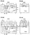
- Figs. 7A to 9B are sectional views of this semiconductor memory device showing the fabrication steps partially.
- a trench 12 is formed at the DRAM region of silicon substrate 1.
- an N type well 1a and a P type well 1b are formed.
- a storage electrode 201 is formed in trench 12.
- a field oxide film 2 for element isolation is formed at the region excluding the element region.
- a capacitor insulating film 202 is formed on storage electrode 201.
- gate oxide film 3 of the memory cell transistor and gate oxide film 3 of the transistor that constitutes the logic circuit are formed.
- cell plate electrode 13 is formed on capacitor insulating film 202.
- gate electrode 14 of the memory cell transistor and gate electrode 14 of the transistor that constitutes the logic circuit are formed.
- an interlayer insulating film 204 is formed all over the DRAM region and logic circuit region. Then, contact holes 16 and 218 are formed at predetermined positions in interlayer insulating film 204 Next, bit line 15 and line 219 are formed. Then, an interlayer insulating film 207 is formed all over the DRAM region and the logic circuit region.
- capacitor insulating film 202 of the memory cell capacitor and gate oxide film 3 of the transistor that forms the logic circuit are provided at the same step, both films have substantially the same thickness. Also, cell plate electrode 13 of the memory cell capacitor is connected to ground line 37. It is therefore not necessary to provide a circuit such as a Vblp generation circuit 41 to supply a cell plate voltage.
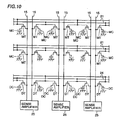
- Fig. 10 is a circuit diagram of a DRAM. Referring to Fig. 10, a plurality of memory cells are arranged in a matrix, each memory cell formed of a memory cell transistor MT and a memory cell capacitor MC. Memory cell transistor MT includes a gate electrode 14 and a semiconductor region 11 isolated by gate electrode 14.
- the threshold value of each memory cell transistor MT is set to a value (approximately 0.4-0.5 V) lower than the threshold value (0.7 V) of the NMOSFET of the logic circuit region. Accordingly, the second term of equation 1 ⁇ becomes smaller to allow increase of the storage capacity.
- the number of memory cell transistors MT connected to the complementary pair of bit lines 15 and 15 is set to not more than 256 in order to maintain the ratio of parasitic capacitance CB of the bit line to capacitance CS of the memory cell capacitor (CB/CS) to 5-15 and ensure the data read out voltage in a memory access operation.
- Memory cell capacitor MC is formed of a storage electrode 201 located in trench 12 and a cell plate electrode 13 covering storage electrode 201, and connected to the source of each memory cell transistor MT by sharing semiconductor region 11.
- Bit line 15 is arranged corresponding to each column of memory cell transistors MT, and connected to the drain of memory cell transistor MT for every one column.
- Two word lines 21 are arranged corresponding to each row of memory cell transistors MT.
- the gates of memory cell transistors MT of two continuous columns are connected to one of the two word lines 21 via intermediate lines 17 and 18. More specifically, one of the two word lines 21 is connected to the gate of memory cell transistors MT arranged at the (4n)th column and the (4n + 1)th column via intermediate line 17, whereas the other of the two word lines 21 is connected to the gate of memory cell transistors MT arranged at the (4n + 2)th column and (4n + 3)th column via intermediate line 18.
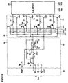
- Fig. 11 is a circuit diagram showing the main part of memory cell array 33.
- memory cell array 33 is formed of two complementary sub arrays 32 (32a, 32b) and a shared sense type sense amplifier band 35 provided therebetween.
- Each of sub arrays 32a and 32b includes a plurality of bit line pairs.
- Sense amplifier band 35 includes a P channel sense amplifier 25Pa provided for every one pair of bit lines 15a1 and 15a2, a P channel sense amplifier 25Pb provided for every one pair of bit lines 15b1 and 15b2, an N channel sense amplifier 25N provided in common to two pairs of bit lines 15a1, 15a2, 15b1 and 15b2, a precharge circuit 43, a local input/output line SubI/O, and a switch circuit 44 to transfer the data on the bit line to input/output line pair SubI/O.
- One sense amplifier 25 of Fig. 10 is formed of one P channel sense amplifier 25Pa or 25Pb and one N channel sense amplifier 25N.
- Each P channel sense amplifier 25Pa is formed of P channel MOSFET (referred to as PMOSFET hereinafter) 45 and 46 having their gates and drains cross-coupled, and set to a latch status.
- Each P channel sense amplifier 25Pb is formed of PMOSFET 60 and 61 having their gates and drains cross-coupled and set in a latch status.
- Each N channel sense amplifier 25N is formed of N channel MOSFET (referred to as NMOSFET hereinafter) 47 and 48 having their gates and drains cross-coupled, and set in a latch status.
- One pair of bit lines 15a1 and 15a2 extending from one sub array 32 is connected to one pair of common bit lines 151 and 152 via switching transistors (NMOSFET) 49 and 50.
- One pair of bit lines 15b1 and 15b2 extending from the other sub array 32b are connected to one pair of common bit lines 151 and 152 via switching transistors (NMOSFET) 58 and 59.
- N channel sense amplifier 25N is connected between common bit lines 151 and 152.
- Switching transistors 49 and 50 have their gates connected in common to a sub array select signal line SBSR.
- switching transistors 49 and 50 have a threshold value identical to that of the NMOSFET employed in the logic circuit region, not the low threshold value as of memory cell transistor MT. Therefore, the voltage amplitude range of SBSR can be set to Vss-Vcc.
- Switching transistors 49 and 50 are located at the opposite side to sub array 32a than P channel sense amplifier 25Pa.
- PMOSFET 45 and 46 have each source connected to local power supply line 36 via drive transistor (NMOSFET) 51.
- NMOSFET drive transistor
- P channel sense amplifiers 25Pa are connected in common to one local power supply line 36.
- Each gate of drive transistor 51 is connected in common to an activation signal line VSPL.
- drive transistor 51 is formed in a step identical to that of memory cell transistor MT, having the threshold value set to the same low threshold value. Therefore, a voltage shifted in level by the threshold value of drive transistor 51 from the level of power supply voltage Vcc can be supplied to bit lines 15a1 and 15a2 of sub array 32a.
- the maximum potential difference between gate electrode 14 connected to word line 21 and bit lines 15a1 and 15a2 can be alleviated.
- the withstand voltage of the gate insulating film of memory cell transistor MT can be ensured to improve the reliability. Also, since the voltage of the higher bit line becomes lower than power supply voltage Vcc by the threshold value of memory cell transistor MT, the restore voltage can be reduced to lower power consumption.
- the voltage amplitude range of an activation signal line VSPL can he set to Vss-Vcc, not Vbb-Vcc. Therefore, only word line 21 is the signal group that has negative bias control. As a result, the additional negative bias control circuit with respect to drive transistor 51 is no longer required, and power consumption can be reduced.
- Power supply voltage Vcc and ground voltage Vss are supplied alternately from DRAM control circuit 39 shown in Fig. 5 to activation signal line VSPL.
- NMOSFET 47 and 48 have each source connected to local ground line 37 via drive transistor (NMOSFET) 52.
- NMOSFET drive transistor
- Four N channel sense amplifiers 25N corresponding to the four P channel sense amplifiers 25Pa connected to one local power supply line 36 are connected in common to one local ground line 37.
- Each gate of drive transistor 52 is connected in common to an activation signal line VSN. More specifically, drive transistors 51 and 52 are turned on by activation signal lines VSPL and VSN, whereby the voltage required for the operation of sense amplifier 25 is supplied.
- Precharge circuit 43 includes an NMOSFET 53 provided between PMOSFET 45 and 46 and NMOSFET 47 and 48 to short-circuit one pair of common bit lines 151 and 152, and NMOSFET 54 and 55 to supply precharge voltage Vblp to bit lines 151 and 152.
- a circuit activation signal SBS power supply voltage Vcc in present embodiment is supplied to NMOSFET 53-55.
- Switch circuit 44 is formed of NMOSFET 56 and 57, and controlled according to a column select signal GYS.
- a column select signal GYS In the present embodiment, four pair of bit lines can be selected by one column select signal GYS. Alternatively, two, eight or more pairs of bit lines can be selected by one column select signal GYS. The data of each bit line pair is connected to input/output line SubI/O via switch circuit 44.
- Switching transistors 58 and 59 have each gate connected in common to a sub array select signal line SBSL.
- PMOSFET 60 and 61 have each source connected in common to local power supply line 36 via drive transistor (NMOSFET) 62.
- NMOSFET drive transistor
- Drive transistor 62 has each gate connected in common to activation signal line VSPR. Similar to drive transistor 51, drive transistor 62 has the threshold value set to a low value in a step identical to that of memory cell transistor MT. Therefore, the voltage amplitude range of sub array select signal line SBSL can be set to Vss-Vcc.
- Fig. 12 is a block diagram showing a row decoder 42 for word line selection.
- Row decoder 42 includes a first row address detection circuit 63, a second row address detection circuit 64, a word line select circuit 65, and a control circuit 66. By this row decoder 42, one word line address is eventually selected out from the four word line addresses selected at first row address detection circuit 63.
- Fig. 13 is a specific circuit diagram of first row address detection circuit 63 and word line select circuit 65.
- First row address detection circuit 63 is formed of three stages of vertical-layered NMOSFET 67a-67c with a row address as the input signal.
- Word line select circuit 65 is formed of a logic circuit 69 and a word line driver 70.
- Logic circuit 69 includes a PMOSFET 71 having a gate connected to a signal supply line (/RDP) to precharge when the row decoder is rendered inactive, NMOSFET 72 and 73 having their gates and drains cross-coupled, and set in a latch status, a PMOSFET 74 having its drain connected to the drain of NMOSFET 73, and having a gate connected to the output terminal of first row address detection circuit 63, a PMOSFET 75 connected between the drain of NMOSFET 72 and the gate of PMOSFET 74, and a PMOSFET 76 having a gate connected to the drain of NMOSFET 73 and a drain connected to the gate of PMOSFET 74.
- a PMOSFET 71 having a gate connected to a signal supply line (/RDP) to precharge when the row decoder is rendered inactive
- NMOSFET 72 and 73 having their gates and drains cross-coupled, and set in a latch status
- Power supply voltage Vcc is applied to the source of each of PMOSFET 71, 74 and 76.
- Ground voltage Vss is applied to the gate of PMOSFET 75.
- Negative voltage Vbb is applied to the source of NMOSFET 72 and 73.
- PMOSFET 75 having its gate connected to round voltage Vss serves to convert the source potential and affirmatively cut off PMOSFET 74.
- Vss round voltage
- the desired operation can be realized without having to use a logic element such as an inverter or the like.
- the number of elements can be reduced to save the area.
- generation of a through current can be prevented in operation transition.
- each word line 21 of sub array 32 is connected the output side of a drive circuit 80 formed of NMOSFET 77 and 78 connected in two stages and an NMOSFET 79 having its drain connected to the output side of NMOSFET 77 and 78.
- Four drive circuits 80 form word line driver 70 as one set.
- NMOSFET 77 of each drive circuit 80 is connected in common to the output end of logic circuit 69.
- the drain of NMOSFET 78 is connected to the four select signal lines SX1-SX4 from control circuit 66.
- NMOSFET 79 of each drive circuit 80 has its gate connected to PMOSFET 71 of logic circuit 69 and has its source applied with negative voltage Vbb. According to the signal from PMOSFET 71 of logic circuit 69, NMOSFET 79 is ON during the inactive state of the row decoder. The potential of word line 21 is maintained at Vbb.
- NMOSFET 77 of each drive circuit 80 is always at a state that can be turned on since power supply voltage Vcc is constantly supplied to the gate.
- each NMOSFET 77 of the four drive circuits 80 are all turned on.
- NMOSFET 78 located as the succeeding stage of NMOSFET 77 attains a state that can be turned on. At this time point, four word lines 21 are selected.
- signal is transferred for only NMOSFET 78 connected to one of the four select signal lines SX1-SX4 from control circuit 66 that is rendered active, whereby eventually one word line 21 is selected.
- negative voltage Vbb is supplied to NMOSFET 72 and 73 of logic circuit 69 and NMOSFET 79 of drive circuit 80.
- the supply line LA from Vbb generation circuit 40 to logic circuit 69 is formed of a line of a different group from the supply line LB from Vbb generation circuit 40 to drive circuit 80 on the layout basis, as shown in Fig. 14.
- supply line LB is provided separately to be impervious to the noise.
- the two stages of NMOSFET 77 and 78 of each drive circuit 80 are set to a low threshold value identical to that of memory cell transistor MT. Therefore, the voltage applied to the gate of NMOSFET 78 (Vcc - the threshold value of NMOSFET 77) is increased and the turn-on time of NMOSFET 78 becomes shorter. As a result, the rising speed of word line 21 becomes faster.
- Fig. 15 is a specific circuit diagram of a redundant row address detection circuit 81 and a word line select circuit 82 in the redundant row decoder.
- Redundant row address detection circuit 81 is formed of the well-known fuse circuit 83 to program a redundancy address.
- Word line select circuit 82 is formed of a logic circuit 84 and a word line driver 85. The structure of word line driver 85 is identical to that of word line driver 70.
- Logic circuit 84 includes a PMOSFET 86 having its gate connected to a signal supply line (/RDP) for precharge when the row decoder is rendered inactive, a PMOSFET 87 having its source connected to the output of redundant address detection circuit 81, its drain connected to the drain of PMOSFET 86, and having a source signal that becomes the first output to word line driver 85, a PMOSFET 88 having its gate connected to the drain of PMOSFET 87, and having a drain signal that becomes the second output to word line driver 85, an NMOSFET 89 having its drain connected to the drain of PMOSFET 88, and a gate connected to the drain of PMOSFET 87, an NMOSFET 90 having its gate connected to the drain of PMOSFET 88, and its drain connected to the drain of PMOSFET 87, and a PMOSFET 91 having its gate connected to the drain of PMOSFET 88, and its drain connected to the source of PMOSFET 87.
- Power supply voltage Vcc is applied to each source of PMOSFET 86, 88 and 91.
- Ground voltage Vss is applied to the gate of PMOSFET 87.
- Negative voltage Vbb is supplied to each source of NMOSFET 89 and 90.
- Fig. 16 is a specific circuit diagram of second row address detection circuit 64 and control circuit 66.
- Second row address detection circuit 64 has four select circuits 64a-64d connected in parallel, formed of a series of a PMOSFET 92 and an NMOSFET 93. Power supply voltage Vcc is applied to the input end of the parallel circuit. The output end is connected to ground voltage Vss (connected to ground) via NMOSFET 95.
- a signal supply line (/RDP) is connected to the gate of PMOSFET 92 of each of select circuits 94a-94d.
- a select signal RAi of word line 21 is applied to the gate of NMOSFET 93 of each of select circuits 94a-94d.
- One of select circuits 94a-94d is identified by this select signal RAi.
- Control circuit 66 is formed of four control circuit units 66a-66d.
- One select signal line (SX1-SX4) is provided from each of control circuit units 66a-66d. This select signal line is connected to a corresponding drive circuit 80 of word line driver 70.
- control circuit unit 66a is connected to the output terminal of select circuit 94a.
- control circuit unit 66b is connected to the output terminal of select circuit 94b.
- control circuit unit 66c is connected to the output terminal of select circuit 94c.
- control circuit unit 66d is connected to the output terminal of select circuit 94d.
- a control circuit unit is identified according to the identified select circuit. As a result, a word line 21 is identified.
- control circuit unit 66a-66d Since the specific circuit structure of each of control circuit units 66a-66d is identical, only the structure of control circuit unit 66a will be described hereinafter.
- a signal XE that allows word line selection (the signal defining the selection period of word line 21) and an inverted signal thereof are applied to a NOR circuit 96.
- An inverted signal of the output from NOR circuit 96 and the output signal from select circuit 94a are applied to an NOR circuit 97.
- Select circuit 94a has its output terminal connected to the drain of PMOSFET 98.
- the inverted signal of the output terminal of select circuit 94a is applied to the gate of PMOSFET 98 and also applied to a NAND circuit 99.
- Signal XE is applied to the other input terminal of NAND circuit 99.
- a signal corresponding to the signal from NAND circuit 99 inverted twice is applied to the source of PMOSFET 100 and the gate of PMOSFET 101.
- NOR circuit 97 has its signal applied to the gate of PMOSFET 100 and an inverted signal thereof applied to the source of PMOSFET 102 and the gate of PMOSFET 103.
- the drain of PMOSFET 102 is connected to the drain of NMOSFET 104 out of NMOSFET 104 and 105 that have their gates and drains cross-coupled and set in a latch status.
- the drain of PMOSFET 103 is connected to the drain of NMOSFET 105.
- PMOSFET 100 has its drain connected to the drain of NMOSFET 106 out of NMOSFET 106 and 107 having their gates and drains cross-coupled and set at a latch state.
- PMOSFET 101 has its drain connected to the drain of NMOSFET 107.
- Select signal line SX1 provided from control circuit unit 66a is connected to the drain of NMOSFET 108.
- NMOSFET 108 has its gate connected to the drain of PMOSFET 103 (the drain of NMOSFET 105). Also, NMOSFET 108 has its drain connected to the drain of PMOSFET 101 (the drain of NMOSFET 107).
- Power supply voltage Vcc is applied to each source of PMOSFET 98, 101 and 103.
- Ground voltage Vss is applied to the gate of PMOSFET 102 and the source of NMOSFET 108.
- Negative voltage Vbb is applied to each source of NMOSFET 104, 105, 106 and 107.
- control circuit unit 66a of the above structure In response to activation of a row address strobe signal /RAS, a signal /RDP attains an H level (logical high) and signal XE attains an H level, whereby the potential of nodes J and K attain an L level (logical low). As a result, PMOSFET 101 is turned on and NMOSFET 107 is turned off, whereby power supply voltage Vcc is supplied to select signal line SX1. Thus, the voltage of word line 21 attains the level of power supply voltage Vcc by word line driver 85 shown in Fig. 15.
- the voltage of the word line is also reduced to the level of ground voltage Vss.
- the potentials of nodes K, L and M all attain an L level.
- NMOSFET 107 is turned on, whereby the voltage of select signal line SX1 is reduced to the level of negative voltage Vbb.
- PMOSFET 103 is turned off.
- NMOSFET 105 is turned on. Therefore, the gate voltage of NMOSFET 108 is reduced to the level of negative voltage Vbb, whereby NMOSFET 108 is turned off.
- the three voltages of negative voltage Vbb, power supply voltage Vcc and round voltage Vss are switched appropriately at control circuit unit 66a to be output through select signal line SX1.
- PMOSFET 103 and NMOSFET 105 are turned on simultaneously, whereby through current I2 flows.
- This flow of through currents I1 and I2 causes a significant increase in negative voltage Vbb.
- Vbb generation circuit 40 must restore the boosted negative voltage Vbb to the level of the predetermined voltage. A great drive capability is required therefor. Also, power consumption is increased.
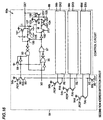
- NMOSFET 109 and 110 are provided at the paths where through currents flow, as shown in Fig. 18.
- PMOSFET 101 and NMOSFET 109 form a CMOS inverter.
- PMOSFET 103 and NMOSFET 110 form a CMOS inverter. Therefore, when the potential of node J is driven to an L level to turn on PMOSFET 101, NMOSFET 109 is turned off. As a result, no through current will flow even if NMOSFET 107 is turned on. Similarly, when the potential of node L is driven to an L level to cause PMOSFET 103 to be turned on, NMOSFET 110 is turned off. As a result, no through current flows even if NMOSFET 105 is turned on.
- Fig 19 shows the arrangement of each structural element of the above semiconductor memory device on a well.
- the semiconductor memory device of the present embodiment is formed on a P type single crystalline silicon substrate or a P type well region (P type substrate region PWA).
- the logic circuit constituted by DRAM control circuit 39, main amplifier I/O system 38, Vbb generation circuit 40, Vblp generation circuit 41, as well as an address buffer, a clock circuit, and the like is formed at an N type well region NWA and a P type substrate region PWA.
- the DRAM core constituted by cell block 32, sense amplifier band 35, row decoder 42 and column decoder 34 is formed at an N type well region NWB deeper than N type well region NWA.
- memory cell array 32 has NMOSFET 47-50 and 52-56 of normal threshold value (identical to the threshold value of the NMOSFET employed in the logic circuit region) provided in a region differing from the region of memory cell transistor MT and NMOSFET 51 and 62 having a threshold value lower than the normal level.
- NMOSFET 47-50 and 52-59 are formed at P type well region PWA whereas memory cell transistor MT and NMOSFET 51 and 62 are formed at P type well region PWB.
- the row decoder has NMOSFET 77 and 78 of word line driver 80 with a low threshold value provided at a different region from the other NMOSFETs.
- NMOSFET 77 and 78 are formed at P type well region PWB.
- the other NMOSFETs are formed at P type well region PWA.
- An address signal is input in synchronization with a rise of row address strobe signal /RAS. More specifically, signal /RDP rises, and then signal XG indicating row address ascertainment rises. The potential of signal line SBS of the precharge circuit falls, and the potential of signal line SBSL falls.
- the level of word line 21 rises to power supply voltage Vcc from negative voltage Vbb. Accordingly, there is a change in the small voltage corresponding to the stored charge of the selected memory cell at one of bit lines 15 forming a pair.
- the rise of the potential of signal line VSP renders sense amplifier 25Pa active, whereby the potential change in the bit line is amplified and provided to input/output line SubI/O.
- signal XE falls, and the potential of word line 21 (select signal line SX1) falls.
- control circuit unit 66a a one shot pulse is generated at node N in response to the fall of signal XE.
- the potential of word line 21 is temporarily held at the level of ground voltage Vss when this one shot pulse is at a high level (power supply voltage Vcc). Then, the voltage of word line 21 falls down to the level of negative voltage Vbb in response to the fall of the one shot pulse.
- Vcc power supply voltage
- Figs. 21A-21C show the potential status of the memory cell in the present embodiment.
- cell plate voltage Vcp and the voltage of P type well region PWB where memory cell transistor MT is formed are both set to the level of ground voltage Vss.
- Fig. 21A shows the write state of an H level (1).
- the gate voltage connected to word line 21 is set to 3.3 V, whereby the H level (2.3 V) of the bit line is written into capacitor MC.
- Fig. 21B shows the write state of an L level (0).
- the gate voltage connected to word line 21 is set to 3.3 V, whereby the L level (0 V) of the bit line is written into memory cell capacitor MC.
- Fig. 21C shows a data retaining state.
- the gate voltage connected to word line 21 is set to -0.5 V which is the nonselected level.
- the bit line is set to the H level/L level of 0 V and 2.3 V in the write/readout state. In a standby state, the bit line is at the level of high precharge voltage 1.2 V.
- the retain voltage of memory cell capacitor MC is 0 V or 2.3 V.
- the source of NMOSFET 79 for address selection is at the level of negative voltage Vbb as described above. Therefore, a reverse bias voltage (-0.5 V) is applied even when the voltage on the bit line or the retain voltage is 0 V. As a result, leakage current that reduces the stored charge will not flow.
- a field effect transistor for use with switching in order to connect the bit line extending from the memory cell array to a sense amplifier can be reliably turned on/off within a small operating range. Therefore, the capability or complexity of the drive circuit can be reduced to allow the area to be saved.
Landscapes
- Engineering & Computer Science (AREA)
- Microelectronics & Electronic Packaging (AREA)
- Computer Hardware Design (AREA)
- Semiconductor Memories (AREA)
- Dram (AREA)
Abstract
Description

Claims (20)
- A semiconductor memory device comprising a first switching transistor (49,50) for connecting a bit line (15a1, 15a2) extending from a memory sub may (32a) including a memory cell transistor(MT) to a first sense amplifier(25Pa,25N), said first switching transistor being arranged at a side opposite to said memory sub array (32a) than the input side of said sense amplifier(25).
- The semiconductor memory device according to claim 1, wherein said first sense amplifier (25Pa,25N) includes a first P channel sense amplifier(25Pa) and an N channel sense amplifier(25N), said first switching transistor (49,50) being arranged between the first P channel sense amplifier(25Pa) and N channel sense amplifier (25N) to effect isolation and connection therebetween.
- The semiconductor memory device according to claim 1, wherein said memory cell transistor(MT) has a threshold value lower than the thresheld value of said first switching transistor(49).
- The semiconductor memory device according to claim 2, further comprising a N channel drive transistor (51) connected between a power supply node (36) and said first P channel sense amplifier(25Pa).
- A semiconductor memory device (31) comprising:a first common bit line (151),a second common bit line (152) complementary to said first common bit line (151),an N channel sense amplifier (25N) connected between said first and second common bit lines (151, 152),a first bit line (15a1),a second bit line (15a2) complementary to said first bit line (15a1),a first P channel sense amplifier (25Pa) connected between said first and second bit lines (15a1, 15a2),a first switching transistor (49) connected between said first common bit line (151) and said first bit line (15a1),a second switching transistor (50) connected between said second common bit line (152) and said second bit line (15a2),a third bit line (14b1),a fourth bit line (15b2) complementary to said third bit line (15b1),a second P channel sense amplifier (25Pb) connected between said third and fourth bit lines (15b1, 15b2),a third switching transistor (58) connected between said first common bit line (151) and said third bit line (15b1),a fourth switching transistor (59) connected between said second common bit line (152) and said fourth bit line (15b2),a word line (21),a memory cell capacitor (MC), anda memory cell transistor (MT) connected between said first bit line (15a1) and said memory cell capacitor (MT), having a gate connected to said word line (21).
- The semiconductor memory device (31) according to claim 5, wherein said memory cell transistor (MT) has a threshold value lower than the threshold value of said first switching transistor (49).
- The semiconductor memory device (31) according to claim 5, further comprising an N channel drive transistor (51) connected between a power supply node (36) and said first P channel sense amplifier (25Pa).
- The semiconductor memory device (31) according to claim 7, wherein said N channel drive transistor (51) has a threshold value lower than the threshold value of said first switching transistor (49).
- The semiconductor memory device (31) according to claim 7, wherein said N channel drive transistor (51) has a threshold value substantially equal to the threshold value of said memory cell transistor (MT).
- The semiconductor memory device (31) according to claim 7, further comprising a control circuit (39) selectively applying a power supply voltage (Vcc) and a ground voltage (Vss) to a gate of said N channel driver transistor (51).
- The semiconductor memory device (31) according to claim 5, wherein each of said sense amplifiers (25Pa, 25Pb, 25N) comprises two sense transistors (45, 46, 60, 61, 47 and 48) that are cross-coupled,
wherein said sense transistor (45, 46, 60, 61, 47 and 48), said memory cell transistor (MT) and said switching transistor (49, 50, 58, 59) have gate insulating films of the same thickness. - The semiconductor memory device (31) according to claim 5, wherein said memory cell transistor (MT) has a back gate connected to ground.
- A semiconductor memory device (31) comprising:a semiconductor substrate (1),a dynamic random access memory formed on said semiconductor substrate (1), anda logic circuit formed on said semiconductor substrate (1) to control said dynamic random access memory,
wherein a memory cell capacitor (MC) in said dynamic random access memory has a capacitor insulating film (202) of a thickness substantially equal to the thickness of a gate insulating film (3) of a transistor that forms said logic circuit. - The semiconductor memory device (31) according to claim 13, wherein said memory cell capacitor (MC) includes a cell plate electrode (13) connected to ground.
- A semiconductor memory device (31) comprising:a power supply line (36),a ground line (37), anda plurality of memory cell arrays (MA00-MAxy), wherein each of said memory cell array (MA00-MAxy) comprisesa sub array (32) including a plurality of bit line pairs (15), anda sense amplifier band (35) adjacent to said sub array (32),
wherein said sense amplifier band (35) comprisesa plurality of P channel sense amplifiers (25Pa, 25Pb) connected to said plurality of bit line pairs (15), respectively,a plurality of power supply drive transistors (51, 62) provided corresponding to said plurality of P channel sense amplifiers (25Pa, 25Pb), each power supply drive transistor being connected between said power supply line (36) and a corresponding P channel sense amplifier (25Pa, 25Pb),a plurality of N channel sense amplifiers (25N) connected to said plurality of bit line pairs (15), respectively, anda plurality of ground drive transistors (52) provided corresponding to said plurality of N channel sense amplifiers (25N), each ground drive transistor being connected between said ground line (37) and a corresponding N channel sense amplifier (25N). - The semiconductor memory device (31) according to claim 15, said plurality of memory cell arrays (MA00-MAxy) being arranged in a matrix, whereinsaid power supply drive transistors (51, 62) in said memory cell array (MA00-MAxy) arranged in each row of said matrix are connected in common to said power supply line (36),said ground drive transistors (52) in said memory cell array (MA00-MAxy) arranged in each row of said matrix are connected in common to said ground line (37),said power supply drive transistors (51, 62) in said memory cell array (MA00-MAxy) arranged in each column of said matrix are connected in common to said power supply line (36), andsaid ground drive transistors (52) in said memory cell array (MA00-MAxy) arranged in each column of said matrix are connected in common to said ground line (37).
- A semiconductor memory device (31) comprising:a word line driver (70) connected to a select signal line (SX1) corresponding to a word line (21) to supply a voltage of said select signal line (SX1) to said word line (21),a row address detection circuit (63) responsive to a row address signal to selectively activate said word line driver (70), anda control circuit (66) responsive to said row address signal to selectively supply a ground voltage or a negative voltage to said select signal line (SX1).
- A semiconductor memory device (31) comprising:a plurality of word line drivers (70), each connected to a plurality of word lines (21) and a plurality of select signal lines (SX1-SX4) corresponding to said plurality of word lines (21) to supply voltages of said plurality of select signal lines (SX1-SX4) to said plurality of word lines (21),a row address detection circuit (63) responsive to a row address signal to selectively activate said plurality of word line drivers (70), anda control circuit (66) responsive to said row address signal to selectively supply a ground voltage or a negative voltage to said plurality of select signal lines (SX1-SX4).
- The semiconductor memory device (31) according to claim 13, wherein said control circuit (66) comprises a plurality of control circuit units (66a-66d) provided corresponding to said plurality of select signal lines (SX1-SX4), each said control circuit unit (66a-66d) includinga first P channel MOS transistor (101) having a gate connected to a first input node (J), a source connected to a power supply node and a drain connected to a corresponding select signal line (SX),a first N channel MOS transistor (107) having a source connected to a negative voltage node, and a drain connected to said corresponding select signal line (SX),a first transmission transistor (100) transmitting a voltage of said first input node (J) to a gate of said first N channel MOS transistor (107),a second N channel MOS transistor (108) having a source connected to ground, and a drain connected to said corresponding select signal line (SX),a second P channel MOS transistor (103) having a gate connected to a second input node (L), a source connected to a power supply node, and a drain connected to a gate of said second N channel MOS transistor (108),a third N channel MOS transistor (105) having a source connected to a negative voltage node and a drain connected to a gate of said second N channel MOS transistor (108), anda second transmission transistor (102) connected between said second input node (L) and a gate of said third N channel MOS transistor (105), turned on constantly.
- The semiconductor memory device (31) according to claim 19, further comprising:a fourth N channel MOS transistor (109) having a gate connected to said first input node (J), a drain connected to the drain of said first P channel MOS transistor (101), and a source connected to the drain of said first N channel MOS transistor (107), anda fifth N channel MOS transistor (110) having a gate connected to said second input node (L), a drain connected to the drain of said second P channel MOS transistor (103), and a source connected to the drain of said third N channel MOS transistor (105).
Applications Claiming Priority (2)
| Application Number | Priority Date | Filing Date | Title |
|---|---|---|---|
| JP8180799 | 1999-03-25 | ||
| JP8180799 | 1999-03-25 |
Publications (2)
| Publication Number | Publication Date |
|---|---|
| EP1039470A2 true EP1039470A2 (en) | 2000-09-27 |
| EP1039470A3 EP1039470A3 (en) | 2000-11-29 |
Family
ID=13756774
Family Applications (1)
| Application Number | Title | Priority Date | Filing Date |
|---|---|---|---|
| EP00106347A Withdrawn EP1039470A3 (en) | 1999-03-25 | 2000-03-23 | Semiconductor memory device |
Country Status (3)
| Country | Link |
|---|---|
| US (2) | US6466502B1 (en) |
| EP (1) | EP1039470A3 (en) |
| KR (1) | KR20000071473A (en) |
Cited By (3)
| Publication number | Priority date | Publication date | Assignee | Title |
|---|---|---|---|---|
| WO2003069676A1 (en) * | 2002-02-14 | 2003-08-21 | Matsushita Electric Industrial Co., Ltd. | Semiconductor device and its manufacturing method |
| WO2003069675A1 (en) * | 2002-02-14 | 2003-08-21 | Matsushita Electric Industrial Co., Ltd. | Semiconductor device and its manufacturing method |
| CN101326632B (en) * | 2005-12-12 | 2012-02-15 | 富士通半导体股份有限公司 | Semiconductor device and manufacturing method thereof |
Families Citing this family (11)
| Publication number | Priority date | Publication date | Assignee | Title |
|---|---|---|---|---|
| JP3853513B2 (en) * | 1998-04-09 | 2006-12-06 | エルピーダメモリ株式会社 | Dynamic RAM |
| KR100403631B1 (en) * | 2001-07-20 | 2003-10-30 | 삼성전자주식회사 | Layout method for bit line sense amplifier driver |
| JP2004140344A (en) * | 2002-09-24 | 2004-05-13 | Toshiba Corp | Semiconductor integrated circuit |
| JP4304697B2 (en) * | 2003-07-30 | 2009-07-29 | インターナショナル・ビジネス・マシーンズ・コーポレーション | Dynamic semiconductor memory device and operation method thereof |
| JP4478982B2 (en) * | 2005-03-16 | 2010-06-09 | エルピーダメモリ株式会社 | Semiconductor memory device |
| JP2009231891A (en) * | 2008-03-19 | 2009-10-08 | Nec Electronics Corp | Semiconductor device |
| KR101157024B1 (en) * | 2010-09-03 | 2012-06-21 | 에스케이하이닉스 주식회사 | Semiconductor Integrated Circuit |
| KR20140042986A (en) * | 2012-09-28 | 2014-04-08 | 삼성전자주식회사 | Memory device having unit cell consisting of single device and method of manufacturing the same |
| WO2015170220A1 (en) * | 2014-05-09 | 2015-11-12 | Semiconductor Energy Laboratory Co., Ltd. | Memory device and electronic device |
| US10991761B2 (en) | 2019-05-13 | 2021-04-27 | Sandisk Technologies Llc | Three-dimensional cross-point memory device containing inter-level connection structures and method of making the same |
| US10879313B2 (en) | 2019-05-13 | 2020-12-29 | Sandisk Technologies Llc | Three-dimensional cross-point memory device containing inter-level connection structures and method of making the same |
Family Cites Families (18)
| Publication number | Priority date | Publication date | Assignee | Title |
|---|---|---|---|---|
| US5732037A (en) | 1982-05-13 | 1998-03-24 | Hitachi, Ltd. | Semiconductor memory |
| JPH07111830B2 (en) | 1989-01-12 | 1995-11-29 | 松下電器産業株式会社 | Semiconductor memory device |
| JP3373534B2 (en) | 1991-07-02 | 2003-02-04 | 株式会社東芝 | Semiconductor storage device |
| EP0559995B1 (en) * | 1992-03-11 | 1998-09-16 | STMicroelectronics S.r.l. | Decoder circuit capable of transferring positive and negative voltages |
| US5323350A (en) | 1992-08-18 | 1994-06-21 | Micron Technologies, Inc. | Integrated circuit memory with dual P-sense amplifiers associated with each column line |
| US5325336A (en) | 1992-09-10 | 1994-06-28 | Mitsubishi Denki Kabushiki Kaisha | Semiconductor memory device having power line arranged in a meshed shape |
| JPH06162779A (en) | 1992-11-24 | 1994-06-10 | Oki Electric Ind Co Ltd | Sense amplifier control circuit in semiconductor memory device |
| US5410508A (en) * | 1993-05-14 | 1995-04-25 | Micron Semiconductor, Inc. | Pumped wordlines |
| US5650976A (en) * | 1993-05-14 | 1997-07-22 | Micron Technology, Inc. | Dual strobed negative pumped wordlines for dynamic random access memories |
| KR960009953B1 (en) | 1994-01-27 | 1996-07-25 | 삼성전자 주식회사 | Sense Amplifier Control Circuit of Semiconductor Memory Device |
| JP3667787B2 (en) | 1994-05-11 | 2005-07-06 | 株式会社ルネサステクノロジ | Semiconductor memory device |
| JPH08297972A (en) | 1995-04-26 | 1996-11-12 | Fujitsu Ltd | Dynamic semiconductor memory device |
| JP2827963B2 (en) | 1995-06-02 | 1998-11-25 | 日本電気株式会社 | Semiconductor integrated circuit device |
| JP3712150B2 (en) | 1996-10-25 | 2005-11-02 | 株式会社日立製作所 | Semiconductor integrated circuit device |
| US5745423A (en) | 1996-12-17 | 1998-04-28 | Powerchip Semiconductor Corp. | Low power precharge circuit for a dynamic random access memory |
| US5774408A (en) | 1997-01-28 | 1998-06-30 | Micron Technology, Inc. | DRAM architecture with combined sense amplifier pitch |
| JPH10241361A (en) | 1997-02-25 | 1998-09-11 | Toshiba Corp | Semiconductor storage device |
| US6046924A (en) * | 1998-06-19 | 2000-04-04 | Kabushiki Kaisha Toshiba | Semiconductor memory device having a sense amplifier region formed in a triple-well structure |
-
2000
- 2000-03-23 EP EP00106347A patent/EP1039470A3/en not_active Withdrawn
- 2000-03-24 KR KR1020000014936A patent/KR20000071473A/en not_active Withdrawn
- 2000-03-24 US US09/537,804 patent/US6466502B1/en not_active Expired - Lifetime
-
2002
- 2002-08-29 US US10/230,187 patent/US20020196690A1/en not_active Abandoned
Cited By (5)
| Publication number | Priority date | Publication date | Assignee | Title |
|---|---|---|---|---|
| WO2003069676A1 (en) * | 2002-02-14 | 2003-08-21 | Matsushita Electric Industrial Co., Ltd. | Semiconductor device and its manufacturing method |
| WO2003069675A1 (en) * | 2002-02-14 | 2003-08-21 | Matsushita Electric Industrial Co., Ltd. | Semiconductor device and its manufacturing method |
| US6974987B2 (en) | 2002-02-14 | 2005-12-13 | Matsushita Electric Industrial Co., Ltd. | Semiconductor device |
| US6995415B2 (en) | 2002-02-14 | 2006-02-07 | Matsushita Electric Industrial Co., Ltd. | Semiconductor device and its manufacturing method |
| CN101326632B (en) * | 2005-12-12 | 2012-02-15 | 富士通半导体股份有限公司 | Semiconductor device and manufacturing method thereof |
Also Published As
| Publication number | Publication date |
|---|---|
| EP1039470A3 (en) | 2000-11-29 |
| US20020196690A1 (en) | 2002-12-26 |
| KR20000071473A (en) | 2000-11-25 |
| US6466502B1 (en) | 2002-10-15 |
Similar Documents
| Publication | Publication Date | Title |
|---|---|---|
| US7639525B2 (en) | Semiconductor memory device | |
| US7199648B2 (en) | Semiconductor integrated circuit including first and second switching transistors having operation states corresponding to operation states of first and second logic circuits | |
| JP3085455B2 (en) | Static RAM | |
| US6972450B2 (en) | SRAM cell design for soft error rate immunity | |
| US6700166B2 (en) | Semiconductor memory device with improved soft-error resistance | |
| US6466502B1 (en) | Semiconductor memory device having switching and memory cell transistors with the memory cell having the lower threshold voltage | |
| US5448518A (en) | Virtual ground type nonvolatile semiconductor memory device capable of simultaneously accessing two memory cells | |
| JP2001338993A (en) | Semiconductor device | |
| KR20020091771A (en) | Semiconductor memory device | |
| JP2003132684A (en) | Semiconductor storage device | |
| GB2162394A (en) | Mos static ram | |
| US6542401B2 (en) | SRAM device | |
| US20020109538A1 (en) | Semiconductor device including a control signal generation circuit allowing reduction in size | |
| US4803664A (en) | Dynamic random access memory having a gain function | |
| EP0444602B1 (en) | Decoder circuit | |
| US10971219B2 (en) | Semiconductor device | |
| US6914797B2 (en) | Semiconductor memory | |
| JP3553850B2 (en) | Semiconductor memory device | |
| US7164593B2 (en) | Semiconductor integrated circuit | |
| JPH0786425A (en) | Dynamic RAM | |
| JP2010267355A (en) | Static random access memory | |
| KR100482370B1 (en) | Semiconductor device having difference thickness of gate oxide | |
| EP0441231B1 (en) | Semiconductor memory device | |
| JPH10162589A (en) | Ferroelectric memory device | |
| US5646895A (en) | Semiconductor memory device with bit line potential compensation circuits |
Legal Events
| Date | Code | Title | Description |
|---|---|---|---|
| PUAI | Public reference made under article 153(3) epc to a published international application that has entered the european phase |
Free format text: ORIGINAL CODE: 0009012 |
|
| AK | Designated contracting states |
Kind code of ref document: A2 Designated state(s): DE FR GB |
|
| AX | Request for extension of the european patent |
Free format text: AL;LT;LV;MK;RO;SI |
|
| PUAL | Search report despatched |
Free format text: ORIGINAL CODE: 0009013 |
|
| RIC1 | Information provided on ipc code assigned before grant |
Free format text: 7G 11C 7/00 A, 7G 11C 11/409 B, 7G 11C 8/00 B, 7G 11C 11/408 B |
|
| AK | Designated contracting states |
Kind code of ref document: A3 Designated state(s): AT BE CH CY DE DK ES FI FR GB GR IE IT LI LU MC NL PT SE |
|
| AX | Request for extension of the european patent |
Free format text: AL;LT;LV;MK;RO;SI |
|
| 17P | Request for examination filed |
Effective date: 20001213 |
|
| AKX | Designation fees paid |
Free format text: DE FR GB |
|
| 17Q | First examination report despatched |
Effective date: 20040102 |
|
| STAA | Information on the status of an ep patent application or granted ep patent |
Free format text: STATUS: THE APPLICATION HAS BEEN WITHDRAWN |
|
| 18W | Application withdrawn |
Effective date: 20040723 |