EP1039347B1 - Antireflective coating for improving cd control - Google Patents
Antireflective coating for improving cd control Download PDFInfo
- Publication number
- EP1039347B1 EP1039347B1 EP00104736A EP00104736A EP1039347B1 EP 1039347 B1 EP1039347 B1 EP 1039347B1 EP 00104736 A EP00104736 A EP 00104736A EP 00104736 A EP00104736 A EP 00104736A EP 1039347 B1 EP1039347 B1 EP 1039347B1
- Authority
- EP
- European Patent Office
- Prior art keywords
- resist
- section
- inorganic
- arc section
- arc
- Prior art date
- Legal status (The legal status is an assumption and is not a legal conclusion. Google has not performed a legal analysis and makes no representation as to the accuracy of the status listed.)
- Expired - Lifetime
Links
Images

Classifications
-
- G—PHYSICS
- G03—PHOTOGRAPHY; CINEMATOGRAPHY; ANALOGOUS TECHNIQUES USING WAVES OTHER THAN OPTICAL WAVES; ELECTROGRAPHY; HOLOGRAPHY
- G03F—PHOTOMECHANICAL PRODUCTION OF TEXTURED OR PATTERNED SURFACES, e.g. FOR PRINTING, FOR PROCESSING OF SEMICONDUCTOR DEVICES; MATERIALS THEREFOR; ORIGINALS THEREFOR; APPARATUS SPECIALLY ADAPTED THEREFOR
- G03F7/00—Photomechanical, e.g. photolithographic, production of textured or patterned surfaces, e.g. printing surfaces; Materials therefor, e.g. comprising photoresists; Apparatus specially adapted therefor
- G03F7/004—Photosensitive materials
- G03F7/09—Photosensitive materials characterised by structural details, e.g. supports, auxiliary layers
- G03F7/091—Photosensitive materials characterised by structural details, e.g. supports, auxiliary layers characterised by antireflection means or light filtering or absorbing means, e.g. anti-halation, contrast enhancement
Definitions
- the invention relates generally to a method for reducing reflectivity in a resist during the fabrication of integrated circuits and more particularly to the improving CD control during patterning.
- ICs semiconductor integrated circuits
- features are formed on a substrate. These features, for example, correspond to devices such as transistors, capacitors, and resistors. These devices are then interconnected to achieve a desired electrical function.
- Lithographic techniques are used to pattern the device layer or layers. Such techniques use an exposure source to project a light image from a mask onto a photoresist (resist) layer formed on the surface of the substrate. The light illuminates the resist layer, exposing it with the desired pattern. Depending on whether a positive or negative tone resist is used, the exposed or unexposed portions of the resist layer are removed. The portions not protected by the resist are then, for example, etched to form the features in the substrate.
- the dimensions of the features depend on the resolution capability of the lithographic systems.
- the minimum feature size (F) achieved by a given generation of lithographic systems is referred to as the lithographic groundrule (GR).
- Critical dimension (CD) is defined as the minimum feature size that must be controlled. This includes, for example, linewidths, spacings, and contact widths.
- CD control Due to the variations of light or reflectance into the resist layer, variations in CD occur. Controlling the variations in CD (CD control) becomes a critical issue, particularly with aggressively shrinking GRs, (e.g., 0.25 microns or below). CD control is facilitated by the use of an antireflective coating (ARC) beneath the resist to reduce reflectance variations into the resist caused by under-lying layers.
- ARC antireflective coating
- the ARC can be used in one of two operational modes to prevent reflectance variations into the resist.
- the first mode is absorption and the second mode is destructive interference.
- the ARC absorbs light passing through it. In this manner, scattering light is prevented from exposing the resist undesirably.
- the ARC should have a suitable extinction coefficient (k) and thickness to absorb the light completely.
- the k and thickness needed to absorb the light completely vary depending on the wavelength of the exposure source. A higher k requires a thinner ARC layer to absorb completely a given amount of light at a given wavelength. Conversely, a lower k would require a thicker ARC layer to absorb completely the given amount of light at the given wavelength. For example, a k of about 0.5 is requires an ARC thickness of about 1000 ⁇ to absorb light at 248 nanometers (nm).
- the reflectance caused by the interface at the bottom surface of the ARC is shifted out of phase with respect to the phase of the reflectance caused by the interface at the top surface of the ARC.
- shifting the reflectances appropriately out of phase with respect to each other they are cancelled out (destructive cancellation).
- Organic ARCs include, for example, compounds presently marketed as AR2 and AR3 by Shipley Company.
- Inorganic ARCs include, for example, silicon nitride, silicon oxynitride, hydrogenated silicon oxynitride, titanium nitride, amorphous silicon, silicon carbide, and amorphous carbon.
- Organic ARCs are usually deposited by a spin-on process.
- Organic ARCs have a relatively fixed refractive index. Different organic ARCs may have different refractive indices. To reduce reflectance at the ARC/resist interface, it is desirable to match the refractive index of the organic ARC with that of the resist. Since organic ARCs have a relatively fixed refractive index, they are usually used only in the absorption mode.
- the film stack beneath the ARC have significant thickness variations due to processing such as, for example, film deposition or chemical mechanical polish (CMP).
- CMP chemical mechanical polish
- a thicker organic ARC is required.
- the use of a thicker organic ARC in turn requires a thicker resist to sufficiently serve as an etch mask during the ARC open process.
- the thicker resist leads to a degradation in the depth-of-focus, particularly at smaller GRs (e.g., 0.25 ⁇ m or less), resulting in a narrowing of the process window. This has made the use of organic ARCs less attractive for processes at GRs of, for example, 0.25 ⁇ m or less.
- Inorganic ARCs have become more popular since they don't have any of the disadvantages associated with organic ARCs. Additionally, inorganic ARCs possess certain advantages such as tunable properties, low defect levels, good conformality, high etch selectivity to resist, and small swing ratio.
- Inorganic ARCs although can be used in either mode, are usually used in the destructive interference mode at the smaller GRs. This is because inorganic ARCs having a sufficiently high k to operate in the absorption mode have a refractive index that does not match the refractive index of the resist. At the smaller GRs, standing waves created by the mismatch in the refractive indices become more pronounced, undesirably resulting in pattern degradation.
- the inorganic ARC In order to produce destructive cancellation when operating in the destructive interference mode, the inorganic ARC needs to be formed on opaque materials or on very uniform transparent materials. In the case where a transparent material such as silicate glass is underneath the inorganic ARC, the thickness variations of the transparent material creates non-uniformities in the intensities of the reflectances. This makes it difficult to take advantage of the destructive interference effect.
- inorganic ARCs can, in some cases, contaminate the resist (resist poisoning) above.
- a cap layer such as silicon oxide (SiO 2 ) may be required to avoid resist poisoning.
- the mismatch in refractive indices between the resist and the cap layer creates standing wave effects in the resist, adversely impacting CD control.
- the invention relates to improved CD control in lithography.
- improved CD control is achieved by using an inorganic ARC having first and second sections.
- the first section operates in the absorption mode and the second section reduces the difference in the refractive indices of the first section and the photoresist, thereby reducing reflectivity in the resist to improve CD control.
- the second section of the inorganic ARC layer comprises a graded refractive index to reduce the difference between the refractive indices between the first section and the resist.
- the refractive index is equal to about the refractive index of the first ARC layer.
- the refractive index as it approaches the upper surface of the second inorganic ARC, gradually decreases to equal to about the refractive index of the resist. Providing a graded refractive index reduces the reflectivity in the resist in order to achieve good CD control.
- the invention relates to semiconductor processing.
- the invention relates to improved CD control, thereby producing a wider lithographic process window.
- improved CD control is achieved by providing an inorganic ARC that combines absorption and destructive interference properties together.
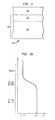
- Fig. 1 shows an ARC layer in accordance with one embodiment of the present invention.
- an ARC layer 130 is provided between the surface of a semiconductor substrate 110 and a resist layer 170.
- the resist layer comprises, for example, any conventional resist used in lithography. Such resist can either be positive or negative tone resist.
- the semiconductor substrate comprises, for example, a silicon wafer.
- Other types of substrates such as those comprising gallium arsenide, germanium, silicon-on-insulator, or other semiconductor or non-semiconductor materials are also useful.
- the substrate can be at various stages of the process flow. For example, the substrate can be at the beginning of the process flow or partially processed to include features (not shown).
- the features are used to form, for example, integrated circuits (ICs) such as dynamic random access memories (DRAMs) or other types of ICs or electromechanical or mechanical devices.
- ICs integrated circuits
- DRAMs dynamic random access memories
- the term "substrate” is used to refer to a substrate in general, which can be at any stage in the process flow.
- the inorganic ARC layer 130 is formed above the substrate.
- the inorganic ARC layer comprises, for example, a dielectric ARC (DARC), metallic ARC, or other inorganic antireflective materials.
- the inorganic ARC comprises DARC such as silicon nitride (Si x N y ), silicon oxynitride, (SiN x O y ), hydrogenated silicon oxynitride or other types of dielectric antireflective materials.
- the DARC comprises silicon oxynitride.
- the inorganic ARC layer is deposited using conventional techniques such as, for example, chemical vapor deposition (CVD).
- the resist is formed over the ARC layer. Any conventional resist material can be used. Typical resist materials comprise an n value of, for example, 1.74.
- the resist is formed by conventional techniques. The thickness of the resist is sufficient to serve as an etch mask for the ARC open process. Typically, the thickness of the resist layer is about 0.2 - 10 ⁇ m.
- the inorganic ARC layer comprises first and second sections 135 and 140.
- the first inorganic ARC section 135 operates in the absorption mode; the second inorganic ARC section 140 reduces the difference in the refractive indices of the first inorganic ARC section and the photoresist.
- Such a configuration reduces reflectivity in the resist, resulting in improved CD control.
- the first inorganic ARC section 135 is in contact with the substrate. Since the first inorganic ARC section operates in the absorption mode, the substrate characteristics do not influence its performance.
- the first inorganic ARC section 135 absorbs substantially all light passing or reflected therein.
- the first inorganic section comprises a k of at least about 0.2 and preferably at least about 0.5.
- the refractive index is dependent on the k.
- the first inorganic ARC section comprises a k of about 0.56 and an n of about 2.1
- the thickness of the first inorganic ARC section should be sufficient to absorb light passing through or reflected therein.
- the thickness in one embodiment, is about 5-150 nm. Of course, the thickness may vary depending on the k value and the amount of light the second ARC section needs to absorb.
- the second inorganic ARC section 140 which is above the first inorganic ARC section, serves to reduce the difference in the refractive indices between two layers, the resist and first inorganic ARC section.
- the difference between the refractive indices of the first inorganic ARC section 135 and the resist is about 0.36 (e.g., 2.1 minus 1.74).
- the second inorganic ARC section reduces the magnitude of this difference (0.36) in order to reduce the reflectivity in the resist.
- the n of the second inorganic ARC section140 is selected to have a value between the refractive indices of the two layers.
- the second inorganic ARC section 140 comprises a graded refractive index.
- the graded refractive index reduces the difference between the refractive indices of the first inorganic ARC section 135 and resist 170.
- the graded refractive index, from the bottom to the top of the second inorganic ARC section decreases from a value equal to about the first inorganic ARC section to a value equal to about the resist.
- Fig. 2a shows a refractive index profile of the second inorganic ARC section 140.
- the first ARC section comprises an n value of about 2.1 and the resist layer comprises an n value of about 1.74. These values are typical for a first inorganic ARC section operating in the absorption mode and a conventional resist.
- the first inorganic ARC section 135 and resist 170 may comprise other n values.
- the second inorganic ARC comprises an n value equal to about the first inorganic ARC section 135.
- the n value in the second inorganic ARC 140 section decreases as you move up through the second inorganic ARC section 140 toward the resist layer 170.
- the n of the second inorganic ARC section 140 decreases to a value equal to about the n of the resist 170 at the interface of the second inorganic ARC section 140 and the resist 170.
- Fig. 2b plots the relationship of the k in the second inorganic ARC section 140 with respect to the n corresponding to the plot in Fig. 2a. As shown, k decreases much more rapidly as the composition of the film is changed to decrease n.
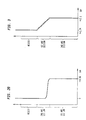
- the graded refractive index of the second inorganic ARC section 140 is shown in Fig. 2a as a smooth transition.
- a second inorganic ARC section 140 comprising a graded refractive index having step transitions is also useful, as shown in Fig. 3.
- the n value in the lower portion of the second inorganic ARC section 140 starts at a value equal to about the first inorganic ARC section and decreases to equal to about the n of the resist in the upper portion.
- the values of n can be varied in the respective portions of the second inorganic ARC section 140.
- n can be greater or less than the n value of first inorganic ARC section 135 or the resist 170 in the lower and upper portions, respectively, of the second inorganic ARC section 140.
- the grade of the refractive index can be varied depending on different parameters, such as thickness or the magnitude of the difference between the refractive indices of the first inorganic ARC section 135 and resist 170. Reduction in reflectivity of the resist is achieved if the difference between the n values of the first inorganic ARC section and resist 170 is reduced.
- Fig. 4 depicts a second inorganic ARC section 140 comprising a graded refractive index that provides an additional interface 141 between the first inorganic ARC section 135 and resist 170.
- the second inorganic ARC section 140 comprises a graded refractive index that is a step function.
- a graded refractive index can be viewed as producing a plurality of sub-sections within the second inorganic ARC section 140, each with a different n value selected so as to reduce the difference in the n values between adjacent sub-sections.
- the difference in the refractive indices between adjacent sub-sections is decreased, thereby decreasing the reflectivity in the resist.
- Increasing the number of sub-sections in the second inorganic ARC section 140 generally further decreases the difference between the n values of adjacent sub-sections, resulting in a greater reduction in the overall reflectivity back into the resist 170.
- the difference in the n values between adjacent sub-sections approaches zero or is infinitesimally small, as in the case where the graded refractive index is continuous and smooth, the overall reflectivity in the top layer or resist 170 approaches zero.
- the second inorganic ARC section 140 can be formed with a graded n having different grades or different number of layers to produce the desired reduction in the difference between the refractive indices of the first inorganic ARC section and resist.
- the number of layers or the specific graded n can be chosen to meet specific needs or optimized for specific processes.
- the second inorganic ARC section 140 should be relatively thin to reduce resist consumption and cost.
- the change in the refractive indices of adjacent subsections does not have to be the same.
- the first and second inorganic ARC section 135, 140 need not comprises the same type of inorganic ARC.
- first and second inorganic ARC sections 135, 140 can be used to form the first and second inorganic ARC sections 135, 140 to achieve a reduction in the refractive indices between the first inorganic ARC section 135, 140 and resist 170. Also, substituting the first inorganic ARC section 135 with an organic ARC can also be useful.
- the deposition of the second inorganic ARC section 140 to produce a graded refractive index can be achieved by tuning the inorganic ARC to have the desired n profile. For example, after deposition of the first inorganic ARC section is completed, the precursor gas flows can be continuously varied during CVD deposition of the second inorganic ARC section 140 to appropriately modify the n. The gas flows can be controlled, for example, to form smooth or stepped transitions in the n profile. Other techniques that modify the refractive index of the second inorganic ARC 140 section can also be used.
- Resist poisoning may occur in some instances, particularly with inorganic ARCS that comprise nitrogen.
- the nitrogen appears to interact with the resist, undesirably affecting the physical properties of the resist.
- a nitrogen-free or reduced nitrogen inorganic ARC sub-section is provided in the upper portion of the second inorganic ARC section 140 to prevent resist poisoning.
- the thickness of the reduced nitrogen or nitrogen-free sub-section should be thin while still capable of preventing resist poisoning. The thickness is, for example, 1 nm or less.
- the inorganic ARC comprises hard mask qualities. Such qualities are particularly useful in, for example, dual-damascene applications.
- the top portion of the second inorganic ARC section 140 comprises an inorganic ARC hard mask sub-section.
- the thickness of the hard mask sub-section should be relatively thin, for example, about 1 nm or less.
- the inorganic ARC hard mask sub-section comprises a silicon-rich material.
- the hard mask sub-section can be formed from, for example, a silicon-based DARC.
- Such silicon-based DARC includes, for example, silicon nitride, silicon oxynitride, or other type of DARC comprising silicon.
- the hard mask portion comprises silicon oxynitride which has its nitrogen component reduced or removed during the deposition process.
- the silicon-rich material can advantageously serve as both a hard mask and to reduce or avoid resist poisoning.
Landscapes
- Engineering & Computer Science (AREA)
- Architecture (AREA)
- Structural Engineering (AREA)
- Physics & Mathematics (AREA)
- General Physics & Mathematics (AREA)
- Exposure Of Semiconductors, Excluding Electron Or Ion Beam Exposure (AREA)
- Photosensitive Polymer And Photoresist Processing (AREA)
- Materials For Photolithography (AREA)
Description
CIRELLI R. A. et al.: "A MULTILAYER INORGANIC ANTIREFLECTIVE SYSTEM FOR USE IN 248 NM DEEP ULTRAVIOLET LITHOGRAPHY", Journal of Vacuum Science and Technology, part B, US, American Institute of Physics, New York, vol. 14, No. 6, 1 Nov. 1996 (1996-11-01). pages 4229-4233, XP000721153 ISSN: 0734-211X and T. TANAKA et al.: "A novel antireflective method with gradient photoabsorption for optical lithography", PROCEEDINGS OD SPIE ― INT. SOC. OPT. ENG., vol 2726, 15 March 1996 (1996-03-15), pages 573-582, XP000905420 USA.
- R =
- reflectivity,
- Iref =
- intensity of reflected light,
- lin =
- intensity of incidence light,
- n1 =
- refractive index of the lower layer,
- n2 =
- refractive index of the upper layer.
- RR =
- the reflectivity into the resist 170,
- R2 =
- the reflectivity into the
upper part 139 of the second inorganic ARC section, - R1 =
- the reflectivity into the
lower part 137 of the second inorganic ARC section, - nR =
- refractive index of the resist
layer 170, - n2 =
- refractive index of the
upper part 139 of the second inorganic ARC section, and - n1 =
- refractive index of the
lower part 137 of the second inorganic ARC section.
Claims (4)
- In lithography, a method for reducing reflectivity in a resist comprising:wherein the ARC comprises a first section (135) and second section (140); the first section (135) operates in absorption mode and the second section (140) comprises a refractive index that reduces a difference between refractive indices of the first section (135) and the resist layer (170),depositing an antireflective, inorganic coating (ARC) over a substrate (110); anddepositing a resist layer (170) over the ARC,
characterized in that
the second ARC section (140) comprises a graded refractive index, wherein graded refractive index at a lower surface of the first ARC section (135) is equal to about the refractive index of the first ARC section (135) and the graded refractive index at an upper surface of the second ARC section (140) is equal to about the resist (170). - The method as recited in claim 1 wherein the first ARC section (135) is deposited over the substrate (110) and the second ARC section (140) is deposited over the first ARC section (135).
- The method as recited in claim 2 wherein the first ARC section (135) comprises an extinction coefficient of at least 0.2.
- The method as recited in claim 1 wherein the second ARC section comprises refractive index between the refractive indices of the first ARC section and resist.
Applications Claiming Priority (2)
| Application Number | Priority Date | Filing Date | Title |
|---|---|---|---|
| US27602699A | 1999-03-25 | 1999-03-25 | |
| US276026 | 1999-03-25 |
Publications (2)
| Publication Number | Publication Date |
|---|---|
| EP1039347A1 EP1039347A1 (en) | 2000-09-27 |
| EP1039347B1 true EP1039347B1 (en) | 2003-12-17 |
Family
ID=23054834
Family Applications (1)
| Application Number | Title | Priority Date | Filing Date |
|---|---|---|---|
| EP00104736A Expired - Lifetime EP1039347B1 (en) | 1999-03-25 | 2000-03-04 | Antireflective coating for improving cd control |
Country Status (6)
| Country | Link |
|---|---|
| EP (1) | EP1039347B1 (en) |
| JP (1) | JP2000299282A (en) |
| KR (1) | KR20000076943A (en) |
| CN (1) | CN1269532A (en) |
| DE (1) | DE60007208T2 (en) |
| TW (1) | TW479293B (en) |
Cited By (1)
| Publication number | Priority date | Publication date | Assignee | Title |
|---|---|---|---|---|
| DE102004036753B4 (en) * | 2004-07-29 | 2008-11-06 | Advanced Micro Devices Inc., Sunnyvale | Process for the preparation of a nitrogen-free ARC topcoat |
Families Citing this family (11)
| Publication number | Priority date | Publication date | Assignee | Title |
|---|---|---|---|---|
| JP2002214793A (en) * | 2001-01-22 | 2002-07-31 | Mitsubishi Electric Corp | Antireflection film and method of manufacturing semiconductor device |
| US6780727B2 (en) * | 2002-04-25 | 2004-08-24 | Chartered Semiconductor Manufacturing Limited | Method for forming a MIM (metal-insulator-metal) capacitor |
| JP3953982B2 (en) | 2002-06-28 | 2007-08-08 | 富士通株式会社 | Semiconductor device manufacturing method and pattern forming method |
| KR100510999B1 (en) * | 2002-07-22 | 2005-08-31 | 주식회사 하이닉스반도체 | Pattern forming method of semiconductor device |
| US20040063001A1 (en) * | 2002-09-30 | 2004-04-01 | Wu Wei E. | Method of making an integrated circuit using a photomask having a dual antireflective coating |
| US6787439B2 (en) * | 2002-11-08 | 2004-09-07 | Advanced Micro Devices, Inc. | Method using planarizing gate material to improve gate critical dimension in semiconductor devices |
| CN100573319C (en) * | 2005-05-27 | 2009-12-23 | 旺宏电子股份有限公司 | Anti-reflective coating and design method thereof |
| JP4563927B2 (en) | 2005-12-02 | 2010-10-20 | 信越化学工業株式会社 | Substrate, manufacturing method thereof, and pattern forming method using the same |
| US20080008837A1 (en) * | 2006-07-10 | 2008-01-10 | Yasuhiro Shiba | Substrate processing apparatus and substrate processing method for heat-treating substrate |
| US8153351B2 (en) * | 2008-10-21 | 2012-04-10 | Advanced Micro Devices, Inc. | Methods for performing photolithography using BARCs having graded optical properties |
| JP5773576B2 (en) * | 2010-04-01 | 2015-09-02 | キヤノン株式会社 | Anti-reflection structure and optical equipment |
-
2000
- 2000-03-04 EP EP00104736A patent/EP1039347B1/en not_active Expired - Lifetime
- 2000-03-04 DE DE2000607208 patent/DE60007208T2/en not_active Expired - Fee Related
- 2000-03-24 KR KR1020000014997A patent/KR20000076943A/en not_active Withdrawn
- 2000-03-27 CN CN00104809A patent/CN1269532A/en active Pending
- 2000-03-27 JP JP2000086623A patent/JP2000299282A/en active Pending
- 2000-03-28 TW TW089105344A patent/TW479293B/en not_active IP Right Cessation
Cited By (1)
| Publication number | Priority date | Publication date | Assignee | Title |
|---|---|---|---|---|
| DE102004036753B4 (en) * | 2004-07-29 | 2008-11-06 | Advanced Micro Devices Inc., Sunnyvale | Process for the preparation of a nitrogen-free ARC topcoat |
Also Published As
| Publication number | Publication date |
|---|---|
| KR20000076943A (en) | 2000-12-26 |
| EP1039347A1 (en) | 2000-09-27 |
| JP2000299282A (en) | 2000-10-24 |
| DE60007208T2 (en) | 2004-11-18 |
| DE60007208D1 (en) | 2004-01-29 |
| TW479293B (en) | 2002-03-11 |
| CN1269532A (en) | 2000-10-11 |
Similar Documents
| Publication | Publication Date | Title |
|---|---|---|
| US6218292B1 (en) | Dual layer bottom anti-reflective coating | |
| JP3321100B2 (en) | Method of forming antireflection layer in semiconductor device | |
| KR100300258B1 (en) | Method and structure for forming integrated circuit pattern on semiconductor substrate | |
| US5674356A (en) | Method for forming a semiconductor device in which an anti reflective layer is formed by varying the composition thereof | |
| KR100307629B1 (en) | Method for forming and applicating a anti reflective film using hydrocarbon based gas | |
| KR100304708B1 (en) | Semiconductor device having a double layer type anti-reflective coating &fabricating method thereof | |
| US20040092089A1 (en) | Polysilicon processing using an anti-reflective dual layer hardmask for 193 nm lithography | |
| EP1016930A1 (en) | Bottom antireflective layer operating in destructive interference and absorption modes | |
| US7901869B2 (en) | Double patterning with a double layer cap on carbonaceous hardmask | |
| US7718345B2 (en) | Composite photoresist structure | |
| EP1039347A1 (en) | Antireflective coating for improving cd control | |
| JP2924791B2 (en) | Photomask and method of manufacturing photomask | |
| US7169514B2 (en) | Extreme ultraviolet mask with molybdenum phase shifter | |
| US8309457B2 (en) | Multilayer low reflectivity hard mask and process therefor | |
| US6143671A (en) | Semiconductor device manufacturing method | |
| KR20000006152A (en) | Method for fabricating semiconductor devices | |
| US6599766B1 (en) | Method for determining an anti reflective coating thickness for patterning a thin film semiconductor layer | |
| KR100242464B1 (en) | Method of forming anti-reflection film of semiconductor device | |
| US6689682B1 (en) | Multilayer anti-reflective coating for semiconductor lithography | |
| US6492701B1 (en) | Semiconductor device having anti-reflective cap and spacer, method of manufacturing the same, and method of manufacturing photoresist pattern using the same | |
| HK1031770A (en) | Arc for improving cd control | |
| JP3608978B2 (en) | Manufacturing method of semiconductor device | |
| KR100516748B1 (en) | Micro pattern formation method of semiconductor device | |
| CN117133712A (en) | Preparation method of semiconductor element | |
| Wang et al. | A novel bottom antireflective coating working for both KrF and ArF excimer laser lithography |
Legal Events
| Date | Code | Title | Description |
|---|---|---|---|
| PUAI | Public reference made under article 153(3) epc to a published international application that has entered the european phase |
Free format text: ORIGINAL CODE: 0009012 |
|
| AK | Designated contracting states |
Kind code of ref document: A1 Designated state(s): DE FR GB IE IT NL |
|
| AX | Request for extension of the european patent |
Free format text: AL;LT;LV;MK;RO;SI |
|
| RIN1 | Information on inventor provided before grant (corrected) |
Inventor name: LU, ZHIJIAN Inventor name: LEE, YONG GILL Inventor name: TOEBBEN, DIRK |
|
| 17P | Request for examination filed |
Effective date: 20001130 |
|
| AKX | Designation fees paid |
Free format text: DE FR GB IE IT NL |
|
| 17Q | First examination report despatched |
Effective date: 20011220 |
|
| GRAP | Despatch of communication of intention to grant a patent |
Free format text: ORIGINAL CODE: EPIDOSNIGR1 |
|
| GRAS | Grant fee paid |
Free format text: ORIGINAL CODE: EPIDOSNIGR3 |
|
| GRAA | (expected) grant |
Free format text: ORIGINAL CODE: 0009210 |
|
| AK | Designated contracting states |
Kind code of ref document: B1 Designated state(s): DE FR GB IE IT NL |
|
| REG | Reference to a national code |
Ref country code: GB Ref legal event code: FG4D |
|
| REG | Reference to a national code |
Ref country code: IE Ref legal event code: FG4D |
|
| REF | Corresponds to: |
Ref document number: 60007208 Country of ref document: DE Date of ref document: 20040129 Kind code of ref document: P |
|
| PGFP | Annual fee paid to national office [announced via postgrant information from national office to epo] |
Ref country code: IE Payment date: 20040218 Year of fee payment: 5 |
|
| RAP2 | Party data changed (patent owner data changed or rights of a patent transferred) |
Owner name: INFINEON TECHNOLOGIES AG |
|
| PGFP | Annual fee paid to national office [announced via postgrant information from national office to epo] |
Ref country code: NL Payment date: 20040227 Year of fee payment: 5 |
|
| PGFP | Annual fee paid to national office [announced via postgrant information from national office to epo] |
Ref country code: GB Payment date: 20040303 Year of fee payment: 5 |
|
| PGFP | Annual fee paid to national office [announced via postgrant information from national office to epo] |
Ref country code: FR Payment date: 20040310 Year of fee payment: 5 |
|
| NLT2 | Nl: modifications (of names), taken from the european patent patent bulletin |
Owner name: INFINEON TECHNOLOGIES AG |
|
| PGFP | Annual fee paid to national office [announced via postgrant information from national office to epo] |
Ref country code: DE Payment date: 20040510 Year of fee payment: 5 |
|
| REG | Reference to a national code |
Ref country code: FR Ref legal event code: TP |
|
| ET | Fr: translation filed | ||
| PLBE | No opposition filed within time limit |
Free format text: ORIGINAL CODE: 0009261 |
|
| STAA | Information on the status of an ep patent application or granted ep patent |
Free format text: STATUS: NO OPPOSITION FILED WITHIN TIME LIMIT |
|
| 26N | No opposition filed |
Effective date: 20040920 |
|
| PG25 | Lapsed in a contracting state [announced via postgrant information from national office to epo] |
Ref country code: IT Free format text: LAPSE BECAUSE OF NON-PAYMENT OF DUE FEES Effective date: 20050304 Ref country code: GB Free format text: LAPSE BECAUSE OF NON-PAYMENT OF DUE FEES Effective date: 20050304 |
|
| PG25 | Lapsed in a contracting state [announced via postgrant information from national office to epo] |
Ref country code: NL Free format text: LAPSE BECAUSE OF NON-PAYMENT OF DUE FEES Effective date: 20051001 Ref country code: DE Free format text: LAPSE BECAUSE OF NON-PAYMENT OF DUE FEES Effective date: 20051001 |
|
| GBPC | Gb: european patent ceased through non-payment of renewal fee |
Effective date: 20050304 |
|
| PG25 | Lapsed in a contracting state [announced via postgrant information from national office to epo] |
Ref country code: FR Free format text: LAPSE BECAUSE OF NON-PAYMENT OF DUE FEES Effective date: 20051130 |
|
| NLV4 | Nl: lapsed or anulled due to non-payment of the annual fee |
Effective date: 20051001 |
|
| REG | Reference to a national code |
Ref country code: IE Ref legal event code: MM4A |
|
| REG | Reference to a national code |
Ref country code: FR Ref legal event code: ST Effective date: 20051130 |