EP1039336A2 - Optical function device - Google Patents
Optical function device Download PDFInfo
- Publication number
- EP1039336A2 EP1039336A2 EP00302210A EP00302210A EP1039336A2 EP 1039336 A2 EP1039336 A2 EP 1039336A2 EP 00302210 A EP00302210 A EP 00302210A EP 00302210 A EP00302210 A EP 00302210A EP 1039336 A2 EP1039336 A2 EP 1039336A2
- Authority
- EP
- European Patent Office
- Prior art keywords
- optical
- function device
- optical function
- optical signal
- rare earth
- Prior art date
- Legal status (The legal status is an assumption and is not a legal conclusion. Google has not performed a legal analysis and makes no representation as to the accuracy of the status listed.)
- Withdrawn
Links
Images


Classifications
-
- G—PHYSICS
- G02—OPTICS
- G02F—OPTICAL DEVICES OR ARRANGEMENTS FOR THE CONTROL OF LIGHT BY MODIFICATION OF THE OPTICAL PROPERTIES OF THE MEDIA OF THE ELEMENTS INVOLVED THEREIN; NON-LINEAR OPTICS; FREQUENCY-CHANGING OF LIGHT; OPTICAL LOGIC ELEMENTS; OPTICAL ANALOGUE/DIGITAL CONVERTERS
- G02F1/00—Devices or arrangements for the control of the intensity, colour, phase, polarisation or direction of light arriving from an independent light source, e.g. switching, gating or modulating; Non-linear optics
- G02F1/35—Non-linear optics
- G02F1/3523—Non-linear absorption changing by light, e.g. bleaching
-
- G—PHYSICS
- G02—OPTICS
- G02F—OPTICAL DEVICES OR ARRANGEMENTS FOR THE CONTROL OF LIGHT BY MODIFICATION OF THE OPTICAL PROPERTIES OF THE MEDIA OF THE ELEMENTS INVOLVED THEREIN; NON-LINEAR OPTICS; FREQUENCY-CHANGING OF LIGHT; OPTICAL LOGIC ELEMENTS; OPTICAL ANALOGUE/DIGITAL CONVERTERS
- G02F3/00—Optical logic elements; Optical bistable devices
-
- H—ELECTRICITY
- H01—ELECTRIC ELEMENTS
- H01S—DEVICES USING THE PROCESS OF LIGHT AMPLIFICATION BY STIMULATED EMISSION OF RADIATION [LASER] TO AMPLIFY OR GENERATE LIGHT; DEVICES USING STIMULATED EMISSION OF ELECTROMAGNETIC RADIATION IN WAVE RANGES OTHER THAN OPTICAL
- H01S3/00—Lasers, i.e. devices using stimulated emission of electromagnetic radiation in the infrared, visible or ultraviolet wave range
- H01S3/05—Construction or shape of optical resonators; Accommodation of active medium therein; Shape of active medium
- H01S3/06—Construction or shape of active medium
- H01S3/063—Waveguide lasers, i.e. whereby the dimensions of the waveguide are of the order of the light wavelength
- H01S3/067—Fibre lasers
- H01S3/06754—Fibre amplifiers
-
- H—ELECTRICITY
- H01—ELECTRIC ELEMENTS
- H01S—DEVICES USING THE PROCESS OF LIGHT AMPLIFICATION BY STIMULATED EMISSION OF RADIATION [LASER] TO AMPLIFY OR GENERATE LIGHT; DEVICES USING STIMULATED EMISSION OF ELECTROMAGNETIC RADIATION IN WAVE RANGES OTHER THAN OPTICAL
- H01S3/00—Lasers, i.e. devices using stimulated emission of electromagnetic radiation in the infrared, visible or ultraviolet wave range
- H01S3/14—Lasers, i.e. devices using stimulated emission of electromagnetic radiation in the infrared, visible or ultraviolet wave range characterised by the material used as the active medium
- H01S3/16—Solid materials
- H01S3/1601—Solid materials characterised by an active (lasing) ion
- H01S3/1603—Solid materials characterised by an active (lasing) ion rare earth
Definitions
- the present invention relates to an optical function device, and more particularly, to a new optical function device which is capable of executing logical operation and optical amplification of optical signal as well as image optical signal and is capable of being operated in a wide temperature range, and thus can be used preferably in optical electronics such as optical communication, optical image processing or optical computer capable of high-level information processing.
- an optical signal is amplified by using an erbium-doped fiber or a crystal, and the optical signal is transferred over a long distance without any electric amplifier, thereby carrying out a high-level information transmission.
- the conventional erbium-doped fiber or crystal has no function of optical operation of an optical signal.
- the conventional optical element using the negative nonlinear absorption (NNA) has no function or effect of optical amplification of an optical signal.
- NNA negative nonlinear absorption
- An optical function device composed of a light transmitting medium containing a rare earth element, comprising a portion thereof doped with 1 x 10 23 per 1 m 3 or more of the rare earth element for executing an inversion of an optical signal, a portion thereof doped with 1 x 10 21 per 1 m 3 or more of the rare earth element for executing an amplification of the optical signal with an excitation light superposed thereto.
- the rare earth element is Er (erbium)
- a wavelength of the optical signal falls in a range of 1.5 ⁇ m ⁇ 1.6 ⁇ m
- a wavelength of the excitation light is 0.98 ⁇ m band or 1.48 ⁇ m band or 0.8 ⁇ m band.
- said optical function device is operated in a temperature range of at least -100 °C ⁇ 300 °C.
- optical signal inversion that is an inversion of intensity of optical signal
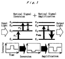
- Fig. 1 shows an energy level structure in the optical signal inversion.
- a light having a wavelength of, for example, 1.53 ⁇ m is irradiated on the optical function device, an electron excites to E 2 level with an absorption cross-sectional area of ⁇ 1 and further excites to E 4 level with an absorption cross-sectional area of ⁇ 2 .
- the excited electron is stored in E 3 level through relaxation.
- the stored electron transits to E 2 level mainly by optical emission.
- an intensity of the incident light is increased, there occurs an increase of the ⁇ 1 and ⁇ 2 and the electron concentration at E 2 level in the emission process, thereby increasing absorption of the incident light (so-called “enhanced absorption”).
- absorption the absorption of the incident light
- the intensity of the incident light is decreased, the enhanced absorption is decreased, thereby increasing the transmitted light.
- NNA negative nonlinear absorption
- optical signal amplification is also carried out as the basic principle. After the optical signal inversion is executed using the negative nonlinear absorption, as shown in Fig. 1, by amplification of the optical signal, that is, optical pumping from E 1 to E 3 , a laser oscillates at transition from E 2 to E 1 .
- an optical-logic-operation element having the optical signal amplification by combining the negative light input-output characteristic and the optical signal amplifying characteristic as described above. This signifies that an element having a function similar to that of a transistor in electronics can be constructed only by an optical signal.
- the rare earth element plays a role of a function element, thus there can be carried out parallel optical operation for operating optical image signals directly by other optical image signals at high density.
- a portion of the optical function device for executing the optical signal inversion is doped with 1 x 10 23 per 1 m 3 or more of a rare earth element
- a portion of the optical function device for executing the optical signal amplification is doped with 1 x 10 21 per 1 m 3 or more of the rare earth element and also is superposed with a excitation light.
- Each portion of the optical function device cannot execute as expected if the rare earth element does not satisfy the above-described doping amounts.
- Pertinent one of the rare earth element may be Er (erbium) since Er is easy to obtain and handle in doping and slso the inversion and amplificaiton can be executed more effectively. But, of course, there may be used other rare earth element besides Er, or two kinds or more of the rare earth elements such as Er.
- a base material containing such a rare earth element may be a crystal such as yttrium aluminum garnet, an amorphous material such as phosphate glass or aluminosilicate glass, or a polymer material.
- a further significant feature of the optical function device of the invention is that the element can be operated in a wide temperature range of at least from -100 °C through 300 °C.
- Fig. 2 shows an outlook view of an optical function device constituted by a crystal (diameter; 10 mm) of erbium yttrium aluminum garnet (Er:YAG).
- the composition of Er:YAG of an optical signal inversion portion (OI portion) having a thickness of 1 mm in the drawing is Er 1.5 Y 1.5 Al 5 O 12 and the composition of an optical signal amplification portion (OA portion) having a thickness of 3 mm is Er 0.5 Y 2.5 Al 5 O 12 .
- An amount of doping Er at the OI portion is about 3 x 10 27 /m 3 and an amount of doping Er at the OA portion is about 1 x 10 27 /m 3 .
- Fig. 3 shows a block schematic diagram of a measuring system.
- a semiconductor laser beam having a wavelength of 1532 nm is used as an input signal light (Laser1) and a laser beam having a wavelength of 1480 nm is superposed as an excitation light (Laser2).
- Other notations in Fig. 3 designate as follows.
- PD1 and PD2 designate optical detectors for monitoring the input signal light and output signal light, respectively.
- D.O. designates a digital oscilloscope for observing waveforms of optical signals. Only the optical signal having the wavelength of 1532 nm is detected as the output signal light.
- Figs. 4(a), 4(b) and 4(c) show detected signal waveforms.
- Fig. 4(a) shows the waveform of the output signal light when the excitation light from the Laser 2 is superposed.
- Fig. 4(b) shows the waveform of the output signal light when the excitation light from the Laser 2 is not superposed.
- Fig. 4(c) shows the waveform of the input signal light from the Laser 1.
- the input signal light of Fig. 4(c) is outputted having its signal intensity inverted as shown in Fig. 4(b) and amplified about 10 times more than the original input intensity as shown in Fig. 4(a) when the excitation light is superposed.
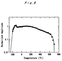
- Fig. 5 shows temperature dependency of the optical function device.
- the ordinate designates an amplitude of a waveform of an inverted output light at respective temperature normalized by dividing it with an amplitude of a waveform of the output light at room temperature.
- the abscissa designates an element temperature. As apparent from Fig. 5, the element is operated in a wide temperature range of -200 °C through 700 °C.
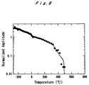
- Fig. 6 shows temperature dependency of the inversion of the optical signal having a wavelength of 1530 nm when the optical function device constituted by a erbium-doped phosphate glass is used.
- a concentration of erbium at the OI portion is about 5 x 10 27 m -3 and its size is 5 x 5 x 5 mm (transmitting length of light is 5 mm).
- the OA portion in not provided.
- the abscissa designates an element temperature and the ordinate designates an amplitude of a waveform of an inverted signal at respective temperature normalized by dividing it with an amplitude of the inverted signal at room temperature.
- the signal inversion in the range of -260 °C to 500 °C is confirmed from the drawing.
- the new optical function device capable of executing logical operation for an optical signal of 1.5 ⁇ m band used in optical communication and has the signal amplification necessary for being connected in multiple stages. Further, the optical function device uses an optical transition of inner-shell in erbium element, thereby being able to be operated in a wide temperature range. Thus, the element is very effective in a space environment where temperature is violently changed.
Landscapes
- Physics & Mathematics (AREA)
- Nonlinear Science (AREA)
- General Physics & Mathematics (AREA)
- Optics & Photonics (AREA)
- Lasers (AREA)
- Optical Modulation, Optical Deflection, Nonlinear Optics, Optical Demodulation, Optical Logic Elements (AREA)
Abstract
Description
- The present invention relates to an optical function device, and more particularly, to a new optical function device which is capable of executing logical operation and optical amplification of optical signal as well as image optical signal and is capable of being operated in a wide temperature range, and thus can be used preferably in optical electronics such as optical communication, optical image processing or optical computer capable of high-level information processing.
- In an optical communication of recent years, an optical signal is amplified by using an erbium-doped fiber or a crystal, and the optical signal is transferred over a long distance without any electric amplifier, thereby carrying out a high-level information transmission.
- On the other hand, there has been developed an optical element for inverting an optical signal by using the negative nonlinear absorption effect of erbium ions (for example, see "All-optical inverter operating over a temperature range of 15-1400K in erbium-doped lutetium aluminum garnet", by Yoshinobu Maeda, Applied Physics Letters, Volume 72, pp395-397).
- However, the conventional erbium-doped fiber or crystal has no function of optical operation of an optical signal. The conventional optical element using the negative nonlinear absorption (NNA) has no function or effect of optical amplification of an optical signal. In addition, there has not been developed, for an optical communication wavelength band (1.5 µm), any optical element capable of controlling an image optical signal directly by another image optical signal and operable in low to high temperatures.
- In view of the foregoing, it is the main object of the present invention to provide a new optical function device which is capable of inverting and amplifying an optical signal of the optical communication wavelength band, and executing operation of an image optical signal, and is operable in a wide temperature range.
- The above and other objects, advantages and features of the present invention are accomplished by a optical function device. An optical function device composed of a light transmitting medium containing a rare earth element, comprising a portion thereof doped with 1 x 10²³ per 1 m3 or more of the rare earth element for executing an inversion of an optical signal, a portion thereof doped with 1 x 10²¹ per 1 m3 or more of the rare earth element for executing an amplification of the optical signal with an excitation light superposed thereto.
- In a further aspect of the invention, the rare earth element is Er (erbium), a wavelength of the optical signal falls in a range of 1.5 µm ∼1.6 µm, and a wavelength of the excitation light is 0.98 µm band or 1.48 µm band or 0.8 µm band.
- In another aspect of the present invention, said optical function device is operated in a temperature range of at least -100 °C∼300 °C.
- Various embodiments of the present invention will now be described, by way of example only, and with reference to the accompanying drawings in which:
- Fig. 1 is a schematic diagram showing optical signal inversion and amplification of an optical function device according to a preferred embodiment.
- Fig. 2 is a perspective outlook view exemplifying a
constitution of an optical function device according to
Embodiment 1 of the invention; - Fig. 3 is a diagram exemplifying a constitution of a measuring system;
- Figs. 4(a), 4(b) and 4(c) are diagrams exemplifying detected signal waveforms;
- Fig. 5 is a diagram exemplifying temperature dependency of the optical function device of the preferred embodiment; and
- Fig. 6 is a diagram exemplifying temperature dependency of the inversion of the optical signal.
-
- According to the optical function device of the invention, firstly, optical signal inversion, that is an inversion of intensity of optical signal, is executed as an important basic principle. Fig. 1 shows an energy level structure in the optical signal inversion. As shown in Fig.1, when a light having a wavelength of, for example, 1.53 µm is irradiated on the optical function device, an electron excites to E2 level with an absorption cross-sectional area of σ1 and further excites to E4 level with an absorption cross-sectional area of σ2. The excited electron is stored in E3 level through relaxation.
- The stored electron transits to E2 level mainly by optical emission. When an intensity of the incident light is increased, there occurs an increase of the σ1 and σ2 and the electron concentration at E2 level in the emission process, thereby increasing absorption of the incident light (so-called "enhanced absorption"). Thus, the light transmitted by the optical function device is decreased. Conversely, when the intensity of the incident light is decreased, the enhanced absorption is decreased, thereby increasing the transmitted light. These phenomenon is called "negative nonlinear absorption" (NNA).
- Consequently, there is realized an inversion of intensity of optical signal in which when the incident light is increased, the transmitted light is decreased, conversely when the incident light is decreased, the transmitted light is increased.
- In addition to the above-described optical signal inversion, according to the invention, optical signal amplification is also carried out as the basic principle. After the optical signal inversion is executed using the negative nonlinear absorption, as shown in Fig. 1, by amplification of the optical signal, that is, optical pumping from E1 to E3, a laser oscillates at transition from E2 to E1.
- Therefore, according to the invention, there can be constructed an optical-logic-operation element having the optical signal amplification by combining the negative light input-output characteristic and the optical signal amplifying characteristic as described above. This signifies that an element having a function similar to that of a transistor in electronics can be constructed only by an optical signal.
- According to the preferred embodiment, the rare earth element plays a role of a function element, thus there can be carried out parallel optical operation for operating optical image signals directly by other optical image signals at high density.
- According to the preferred embodiment, a portion of the optical function device for executing the optical signal inversion is doped with 1 x 10²³ per 1 m3 or more of a rare earth element, and a portion of the optical function device for executing the optical signal amplification is doped with 1 x 10²¹ per 1 m3 or more of the rare earth element and also is superposed with a excitation light. Each portion of the optical function device cannot execute as expected if the rare earth element does not satisfy the above-described doping amounts.
- Pertinent one of the rare earth element may be Er (erbium) since Er is easy to obtain and handle in doping and slso the inversion and amplificaiton can be executed more effectively. But, of course, there may be used other rare earth element besides Er, or two kinds or more of the rare earth elements such as Er.
- A base material containing such a rare earth element may be a crystal such as yttrium aluminum garnet, an amorphous material such as phosphate glass or aluminosilicate glass, or a polymer material.
- A further significant feature of the optical function device of the invention is that the element can be operated in a wide temperature range of at least from -100 °C through 300 °C.
- Fig. 2 shows an outlook view of an optical function device constituted by a crystal (diameter; 10 mm) of erbium yttrium aluminum garnet (Er:YAG). The composition of Er:YAG of an optical signal inversion portion (OI portion) having a thickness of 1 mm in the drawing is Er1.5Y1.5Al5O12 and the composition of an optical signal amplification portion (OA portion) having a thickness of 3 mm is Er0.5Y2.5Al5O12. An amount of doping Er at the OI portion is about 3 x 1027/m3 and an amount of doping Er at the OA portion is about 1 x 1027/m3.
- Fig. 3 shows a block schematic diagram of a measuring system. As shown in Fig. 3, a semiconductor laser beam having a wavelength of 1532 nm is used as an input signal light (Laser1) and a laser beam having a wavelength of 1480 nm is superposed as an excitation light (Laser2). Other notations in Fig. 3 designate as follows. PD1 and PD2 designate optical detectors for monitoring the input signal light and output signal light, respectively. D.O. designates a digital oscilloscope for observing waveforms of optical signals. Only the optical signal having the wavelength of 1532 nm is detected as the output signal light.
- Figs. 4(a), 4(b) and 4(c) show detected signal waveforms. Fig. 4(a) shows the waveform of the output signal light when the excitation light from the
Laser 2 is superposed. Fig. 4(b) shows the waveform of the output signal light when the excitation light from theLaser 2 is not superposed. Fig. 4(c) shows the waveform of the input signal light from theLaser 1. As is apparent from the drawings, the input signal light of Fig. 4(c) is outputted having its signal intensity inverted as shown in Fig. 4(b) and amplified about 10 times more than the original input intensity as shown in Fig. 4(a) when the excitation light is superposed. - When the optical function device in Fig. 3 was changed to an element constituted only by the OI portion (no OA portion), the phenomenon of inverting the optical signal was obtained, but the signal could not be amplified even when the excitation light is superposed thereon. On the other hand, when an element constituted only by the OA portion (no OI portion) was used, the optical signal was not inverted.
- Fig. 5 shows temperature dependency of the optical function device. The ordinate designates an amplitude of a waveform of an inverted output light at respective temperature normalized by dividing it with an amplitude of a waveform of the output light at room temperature. The abscissa designates an element temperature. As apparent from Fig. 5, the element is operated in a wide temperature range of -200 °C through 700 °C.
- Fig. 6 shows temperature dependency of the inversion of the optical signal having a wavelength of 1530 nm when the optical function device constituted by a erbium-doped phosphate glass is used. A concentration of erbium at the OI portion is about 5 x 1027 m-3 and its size is 5 x 5 x 5 mm (transmitting length of light is 5 mm). In this example, the OA portion in not provided. The abscissa designates an element temperature and the ordinate designates an amplitude of a waveform of an inverted signal at respective temperature normalized by dividing it with an amplitude of the inverted signal at room temperature. The signal inversion in the range of -260 °C to 500 °C is confirmed from the drawing.
- As has been explained in details, according to the preferred embodiment, there is provided the new optical function device capable of executing logical operation for an optical signal of 1.5 µm band used in optical communication and has the signal amplification necessary for being connected in multiple stages. Further, the optical function device uses an optical transition of inner-shell in erbium element, thereby being able to be operated in a wide temperature range. Thus, the element is very effective in a space environment where temperature is violently changed.
- While the invention has been described in detail and with reference to specific embodiments thereof, it will be apparent to one skilled in the art that various changes and modifications can be made.
Claims (10)
- An optical function device composed of a light transmitting medium containing a rare earth element, comprising:a portion (OI) thereof doped with 1 x 10²³ per 1 m3 or more of the rare earth element for inverting an optical signal; anda portion (OA) thereof doped with 1 x 10²¹ per 1 m3 or more of the rare earth element for amplifying the optical signal with an excitation light superposed thereto.
- The optical function device as claimed in claim 1, wherein the rare earth element is erbium (Er).
- The optical function device as claimed in claim 1 or 2, wherein a wavelength of the optical signal falls in the range of 1.5 µm ∼ 1.6 µm.
- The optical function device as claimed in claim 1, 2, or 3, wherein a wavelength of the excitation light is 0.98 µm band.
- The optical function device as claimed in claim 1, 2, or 3, wherein a wavelength of the excitation light is 1.48 µm band.
- The optical function device as claimed in claim 1, 2, or 3, wherein a wavelength of the excitation light is 0.8 µm band.
- The optical function device as claimed in any preceding claim, wherein said optical function device is operable in a temperature range of at least -100 °C ∼ 300 °C.
- The optical function device as claimed in any preceding claim, wherein said optical function device comprises yttrium aluminum garnet, a phosphate glass, an aluminosilicate glass, or a polymer material.
- The optical function device as claimed in any preceding claim, wherein said portion (OI) for inverting the optical signal is doped with at least 3 x 1027/m3 erbium.
- The optical function device as claimed in any preceding claim, wherein said portion (OA) for amplifying the optical signal is doped with at least 1 x 1027/m3 erbium.
Applications Claiming Priority (2)
| Application Number | Priority Date | Filing Date | Title |
|---|---|---|---|
| JP11693499 | 1999-03-20 | ||
| JP11116934A JP2000275693A (en) | 1999-03-20 | 1999-03-20 | Optical function element |
Publications (2)
| Publication Number | Publication Date |
|---|---|
| EP1039336A2 true EP1039336A2 (en) | 2000-09-27 |
| EP1039336A3 EP1039336A3 (en) | 2003-01-02 |
Family
ID=14699329
Family Applications (1)
| Application Number | Title | Priority Date | Filing Date |
|---|---|---|---|
| EP00302210A Withdrawn EP1039336A3 (en) | 1999-03-20 | 2000-03-17 | Optical function device |
Country Status (3)
| Country | Link |
|---|---|
| US (1) | US6353498B1 (en) |
| EP (1) | EP1039336A3 (en) |
| JP (1) | JP2000275693A (en) |
Families Citing this family (4)
| Publication number | Priority date | Publication date | Assignee | Title |
|---|---|---|---|---|
| US7459781B2 (en) * | 2003-12-03 | 2008-12-02 | Wen-Kun Yang | Fan out type wafer level package structure and method of the same |
| US7514767B2 (en) * | 2003-12-03 | 2009-04-07 | Advanced Chip Engineering Technology Inc. | Fan out type wafer level package structure and method of the same |
| JP4977283B2 (en) * | 2004-07-12 | 2012-07-18 | オプトトライオード株式会社 | Optical signal amplifier |
| US7417788B2 (en) * | 2005-11-21 | 2008-08-26 | Aditya Narendra Joshi | Optical logic device |
Family Cites Families (4)
| Publication number | Priority date | Publication date | Assignee | Title |
|---|---|---|---|---|
| US5406420A (en) * | 1992-06-15 | 1995-04-11 | Research Development Corporation Of Japan | Optical device |
| US5537243A (en) * | 1993-12-17 | 1996-07-16 | At&T Corp. | All-optical flip-flop |
| US5434701A (en) * | 1993-12-17 | 1995-07-18 | At&T Corp. | All-optical inverter |
| JP3358770B2 (en) * | 1995-07-10 | 2002-12-24 | 科学技術振興事業団 | Light control substance and light control method |
-
1999
- 1999-03-20 JP JP11116934A patent/JP2000275693A/en active Pending
-
2000
- 2000-03-17 EP EP00302210A patent/EP1039336A3/en not_active Withdrawn
- 2000-03-17 US US09/531,123 patent/US6353498B1/en not_active Expired - Fee Related
Non-Patent Citations (3)
| Title |
|---|
| DATABASE INSPEC [online] THE INSTITUTION OF ELECTRICAL ENGINEERS, STEVENAGE, GB; MAEDA Y.: "Negative nonlinear absorption effect in the excited state absorption of the Er<3+> ion", Database accession no. 6237883 * |
| MAEDA Y.: "Negative nonlinear absorption effect in the excited state absorption of the Er<3+> ion", OYO BUTURI, JAPAN SOC. APPL. PHYS, vol. 68, no. 1, January 1999 (1999-01-01), JAPAN, pages 33 - 37, XP009064461 * |
| MIYAZAKI Y.; SOMA T.; BALASUBRAMANIAN R.: "Optical properties of integrated type amplifiers using erbium doped crystal film waveguides", INTERNATIONAL TOPICAL MEETING ON MICROWAVE PHOTONICS. MWP '96 TECHNICAL DIGEST. SATELLITE WORKSHOP (CAT. NO.96TH8153), 1996, NEW YORK, NY, USA * |
Also Published As
| Publication number | Publication date |
|---|---|
| US6353498B1 (en) | 2002-03-05 |
| JP2000275693A (en) | 2000-10-06 |
| EP1039336A3 (en) | 2003-01-02 |
Similar Documents
| Publication | Publication Date | Title |
|---|---|---|
| JP2957719B2 (en) | Optical fiber amplifier | |
| JP2849700B2 (en) | Optical transmission method, information transmission method, and optical transmission device | |
| Park et al. | Laser action in Eu-doped GaN thin-film cavity at room temperature | |
| CN101527423B (en) | High-mean-power high-repetition-rate solid laser | |
| US6218658B1 (en) | Optical fuse | |
| Wang et al. | High‐Gain Waveguide Amplifiers in Ge25Sb10S65 Photonics Heterogeneous Integration with Erbium‐Doped Al2O3 Thin Films | |
| US7813614B2 (en) | Amplifying optical fiber | |
| JP3299684B2 (en) | Optical amplifier and optical amplification method | |
| US5341237A (en) | Rare earth ion doped optical element | |
| EP1039336A2 (en) | Optical function device | |
| EP0426222B1 (en) | Active fiber optical amplifier having a wide band signal wavelength | |
| US6404785B1 (en) | Solid state modulated ultraviolet laser | |
| Chen et al. | Optical gain from InAs nanocrystal quantum dots in a polymer matrix | |
| US20090034060A1 (en) | Optical fiber element and method for imparting non-reciprocity of light using the same | |
| JP3600872B2 (en) | Rare earth element doped Si material and manufacturing method thereof | |
| JP3412712B2 (en) | Crystal materials for solid-state lasers | |
| KR100266300B1 (en) | Light control material and light control method using same | |
| EP3719941B1 (en) | Planar waveguide and laser amplifier | |
| US5406420A (en) | Optical device | |
| KR101188039B1 (en) | A raman diffusion optical amplifier | |
| EP1317037A3 (en) | Optical amplifier | |
| JPH07249811A (en) | Direct light amplifier | |
| JPH01145885A (en) | optical amplifier | |
| JP3296195B2 (en) | Laser, optical amplifier, and optical amplification method | |
| WADA et al. | Amplification characteristics of waveguide type optical amplifier using Nd doped garnet thin film |
Legal Events
| Date | Code | Title | Description |
|---|---|---|---|
| PUAI | Public reference made under article 153(3) epc to a published international application that has entered the european phase |
Free format text: ORIGINAL CODE: 0009012 |
|
| AK | Designated contracting states |
Kind code of ref document: A2 Designated state(s): AT BE CH CY DE DK ES FI FR GB GR IE IT LI LU MC NL PT SE |
|
| AX | Request for extension of the european patent |
Free format text: AL;LT;LV;MK;RO;SI |
|
| PUAL | Search report despatched |
Free format text: ORIGINAL CODE: 0009013 |
|
| AK | Designated contracting states |
Kind code of ref document: A3 Designated state(s): AT BE CH CY DE DK ES FI FR GB GR IE IT LI LU MC NL PT SE |
|
| AX | Request for extension of the european patent |
Free format text: AL;LT;LV;MK;RO;SI |
|
| RIC1 | Information provided on ipc code assigned before grant |
Free format text: 7G 02F 3/02 A, 7G 02F 1/35 B, 7G 02F 1/355 B |
|
| RAP1 | Party data changed (applicant data changed or rights of an application transferred) |
Owner name: TOYOTA JIDOSHA KABUSHIKI KAISHA Owner name: NATIONAL SPACE DEVELOPMENT AGENCY OF JAPAN Owner name: THE JAPAN SPACE FORUM Owner name: TOYOTA SCHOOL FOUNDATION |
|
| 17P | Request for examination filed |
Effective date: 20030624 |
|
| AKX | Designation fees paid |
Designated state(s): DE FR GB |
|
| STAA | Information on the status of an ep patent application or granted ep patent |
Free format text: STATUS: THE APPLICATION IS DEEMED TO BE WITHDRAWN |
|
| 18D | Application deemed to be withdrawn |
Effective date: 20061024 |