EP1039330A2 - Optical waveguide isolator - Google Patents
Optical waveguide isolator Download PDFInfo
- Publication number
- EP1039330A2 EP1039330A2 EP00302255A EP00302255A EP1039330A2 EP 1039330 A2 EP1039330 A2 EP 1039330A2 EP 00302255 A EP00302255 A EP 00302255A EP 00302255 A EP00302255 A EP 00302255A EP 1039330 A2 EP1039330 A2 EP 1039330A2
- Authority
- EP
- European Patent Office
- Prior art keywords
- layer
- light
- optical
- magnetic
- magnetic material
- Prior art date
- Legal status (The legal status is an assumption and is not a legal conclusion. Google has not performed a legal analysis and makes no representation as to the accuracy of the status listed.)
- Granted
Links
Images

Classifications
-
- H—ELECTRICITY
- H01—ELECTRIC ELEMENTS
- H01S—DEVICES USING THE PROCESS OF LIGHT AMPLIFICATION BY STIMULATED EMISSION OF RADIATION [LASER] TO AMPLIFY OR GENERATE LIGHT; DEVICES USING STIMULATED EMISSION OF ELECTROMAGNETIC RADIATION IN WAVE RANGES OTHER THAN OPTICAL
- H01S5/00—Semiconductor lasers
- H01S5/50—Amplifier structures not provided for in groups H01S5/02 - H01S5/30
-
- G—PHYSICS
- G02—OPTICS
- G02F—OPTICAL DEVICES OR ARRANGEMENTS FOR THE CONTROL OF LIGHT BY MODIFICATION OF THE OPTICAL PROPERTIES OF THE MEDIA OF THE ELEMENTS INVOLVED THEREIN; NON-LINEAR OPTICS; FREQUENCY-CHANGING OF LIGHT; OPTICAL LOGIC ELEMENTS; OPTICAL ANALOGUE/DIGITAL CONVERTERS
- G02F1/00—Devices or arrangements for the control of the intensity, colour, phase, polarisation or direction of light arriving from an independent light source, e.g. switching, gating or modulating; Non-linear optics
- G02F1/01—Devices or arrangements for the control of the intensity, colour, phase, polarisation or direction of light arriving from an independent light source, e.g. switching, gating or modulating; Non-linear optics for the control of the intensity, phase, polarisation or colour
- G02F1/09—Devices or arrangements for the control of the intensity, colour, phase, polarisation or direction of light arriving from an independent light source, e.g. switching, gating or modulating; Non-linear optics for the control of the intensity, phase, polarisation or colour based on magneto-optical elements, e.g. exhibiting Faraday effect
- G02F1/095—Devices or arrangements for the control of the intensity, colour, phase, polarisation or direction of light arriving from an independent light source, e.g. switching, gating or modulating; Non-linear optics for the control of the intensity, phase, polarisation or colour based on magneto-optical elements, e.g. exhibiting Faraday effect in an optical waveguide structure
- G02F1/0955—Devices or arrangements for the control of the intensity, colour, phase, polarisation or direction of light arriving from an independent light source, e.g. switching, gating or modulating; Non-linear optics for the control of the intensity, phase, polarisation or colour based on magneto-optical elements, e.g. exhibiting Faraday effect in an optical waveguide structure used as non-reciprocal devices, e.g. optical isolators, circulators
-
- H—ELECTRICITY
- H01—ELECTRIC ELEMENTS
- H01S—DEVICES USING THE PROCESS OF LIGHT AMPLIFICATION BY STIMULATED EMISSION OF RADIATION [LASER] TO AMPLIFY OR GENERATE LIGHT; DEVICES USING STIMULATED EMISSION OF ELECTROMAGNETIC RADIATION IN WAVE RANGES OTHER THAN OPTICAL
- H01S5/00—Semiconductor lasers
- H01S5/005—Optical components external to the laser cavity, specially adapted therefor, e.g. for homogenisation or merging of the beams or for manipulating laser pulses, e.g. pulse shaping
- H01S5/0064—Anti-reflection components, e.g. optical isolators
-
- H—ELECTRICITY
- H01—ELECTRIC ELEMENTS
- H01S—DEVICES USING THE PROCESS OF LIGHT AMPLIFICATION BY STIMULATED EMISSION OF RADIATION [LASER] TO AMPLIFY OR GENERATE LIGHT; DEVICES USING STIMULATED EMISSION OF ELECTROMAGNETIC RADIATION IN WAVE RANGES OTHER THAN OPTICAL
- H01S5/00—Semiconductor lasers
- H01S5/02—Structural details or components not essential to laser action
- H01S5/026—Monolithically integrated components, e.g. waveguides, monitoring photo-detectors, drivers
Definitions
- the present invention relates to an optical isolator, especially an optical waveguide capable of being integrated on a substrate together with a semiconductor laser and an optical waveguide.
- an optical isolator In optical communication systems, an optical isolator is used to prevent reflected light and scattered light in the end face of the optical fiber from returning to a light source side.
- An optical isolator using a rotation of the polarization plane according to the magneto-optic material has been put to practical use as an optical isolator.
- the optical isolator of the Faraday rotation type is constituted by a polarizer, a Faraday rotator of optically transparent material and an analyzer, so that polarized components corresponding to the plane of polarization of the polarizer out of advanced circular polarization of light to the forward direction pass through the polarizer, the plane of polarization is rotated by the Faraday rotator by 45°, and they emanate by passing the analyzer which is inclined at the polarizer by 45°.
- the return light propagated in the direction opposite to the forward direction is obstructed by the polarizer, since after passing the analyzer, the plane of polarization of the return light receives another rotation of 45° by the Faraday rotator and returns to the polarizer.
- the polarized beam splitter and the double refraction prism are utilized as polarizer and analyzer in conventional optical waveguide isolators.
- the above well known optical waveguide isolator was not able to be manufactured with a semiconductor optical element such as semiconductor lasers and optical modulators as one body, since the known optical waveguide isolator does not have the same kind of structure as a semiconductor device. Therefore, the well known optical waveguide isolator must be made as another discrete structure with the substrate of the optical circuit to which the semiconductor device such as semiconductor lasers is integrated, so that the manufacturing step becomes complicated and the manufacturing cost becomes high. Particularly, phase-matching is necessary, and precise processing is necessary, so that the manufacturing process becomes complex. On the other hand, if the optical waveguide isolator could be formed on the substrate by using the same semiconductor manufacturing technology as semiconductor devices such as semiconductor lasers and photodiodes, it could be manufactured with precise manufacturing steps and thus the manufacturing cost could be substantially reduced.
- an optical isolator comprising: a semiconductor optical amplifier structure including a semiconductor substrate of a first conductivity type (that is, n-type or p-type) having a surface of a layer to be formed thereon, a first cladding layer of the first conductivity type formed on the substrate, an active layer formed on the first cladding layer, a second cladding layer of the second conductivity type, opposite to the first conductivity type, formed on the active layer, a first electrode formed on the surface of the semiconductor substrate opposite to the surface to be formed as a layer, and a second electrode formed on the second cladding layer; wherein the first and the second cladding layers and the active layer form an optical waveguide in which the light wave propagates, the semiconductor optical amplifier structure further comprises a light-absorptive magnetic material layer having a light absorption function for the light wave propagating through the optical waveguide, the magnetic material layer is magnetized so as to have the magnetic field component in the direction that corresponds to the direction of the magnetic vector of the
- the present invention is based on the recognition that the refractive index, that is, the equivalent refractive index for the light wave propagating in die optical waveguide, can be changed in the entire waveguide according to the propagating direction of the light wave by using the magneto-optical or Kerr effect. If the equivalent refractive index can be changed according to the propagating direction of the light wave, the attenuation of the light wave propagated in one direction and the attenuation of the light wave propagated in the opposite direction can be made different, and thus an optical waveguide isolator can be constructed by using the difference in attenuation when the light wave propagates in the optical waveguide.
- an optical absorptive magnetic material layer is formed on the optical waveguide and the optical absorptive magnetic material layer is magnetized in the direction corresponding to direction of vibration of the magnetic vector of the light wave propagating the optical waveguide.
- the light wave propagates in the optical absorptive magnetic material layer of the optical waveguide, so that the propagated light wave is subjected to the magneto-optic effect of the optical absorptive magnetic material layer as the entire waveguide structure, and thus not only the real but also the imaginary part of the refractive index becomes nonreciprocal (i.e.
- the amount of the attenuation can differ only by appropriately setting the magnetizable direction of the magnetic material layer according to the direction of propagation. As a result, a complicated structure for phase matching and precise processing steps become unnecessary.
- the nonreciprocity of the optical waveguide structure according to embodiments of the present invention is explained theoretically due to the magnet-optical effect thereof.
- an xyz coordinate system described later and shown in Fig. 1 (the propagating direction of the light wave is assumed to be the z direction and the directions orthogonal to the propagating direction of the light wave are assumed to be the x and y directions) is assumed.
- the character of the magneto-optic material is shown by the dielectric tensor, and when magnetic material formed on the waveguide is not magnetized, the permittivity F is shown by the following expression:
- ⁇ 0 shows the permittivity in the vacuum.
- the dielectric tensor is symmetric, and thus does not bring about nonreciprocity of the light wave into which the equivalent refractive index therefore changes according to the propagating direction of the light wave.
- ⁇ n+i ⁇ k shows the changed portion of the equivalent refractive index
- K 0 is the wave number of light in the vacuum
- n is the refractive index of each layer of the waveguide
- H y is a magnetic-field component of the transverse magnetic mode of the magnetic material formed on the waveguide.
- the changed component of the equivalent refractive index to the light wave propagated in the - z direction is the same as to residual elements, except only that the sign of the term of ⁇ xz of the integration term at the right of expression (3) reverses. Therefore, the equivalent refractive index will differ between the travelling wave and the returning wave.
- the incident signal light can be output with light amplification by assuming the optical waveguide structure to be a semiconductor optical amplifier structure so as to compensate the attenuation amount of the signal light caused as the signal light propagates in the waveguide, so that the isolation function can be achieved without attenuating the signal light.
- L is the length of the device. It was confirmed to be possible to obtain an isolation ratio of 40dB in a length of the device of about 2.0 mm since the optical waveguide isolator explained by the embodiment described later was simulated.
- the first light wave is a signal light to be transmitted along a transmission system
- the second light wave is the return light propagated in the direction opposite to the signal light.
- the signal light to be transmitted is not so attenuated, and the return light such as reflected light and the scattered light caused in transmission path can be greatly attenuated.
- the optical absorption magnetic material layer is constituted by magnetic material magnetized so as to have the magnetic-field component in the direction corresponding to the vibrating direction of a magnetic vector of the first light wave propagating on the waveguide.
- the direction of the external magnetic field should be made to correspond to the vibrating direction of the magnetic vector of the light wave having various modes propagating on the waveguide; for example, the magnetic material layer is formed in the case of the transverse magnetic mode light along the plane parallel to the substrate, so that the nonreciprocity according to the magnetoptical effect can be achieved by magnetizing the magnetic material layer in a direction orthogonal to the propagating direction of the light wave.
- optical absorption magnetic material which causes the magneto-optical effect
- ferromagnetic materials of nickel, iron, and cobalt, etc. and various magnetic materials such as yttrium iron garnet (YIG) can be used.
- YIG yttrium iron garnet
- this substrate is a semiconductor substrate, and the core layer and first and second cladding layers are likewise constituted of semiconductor material. According to such a constitution, the optical waveguide isolator can be formed on the same semiconductor substrate with a semiconductor laser by using the usual semiconductor manufacturing technology.
- an optical waveguide isolator comprising a semiconductive light amplifier structure including a semiconductor substrate of a first conductivity type having a surface of a layer to be formed, a first cladding layer of the first conductivity type formed on the substrate, an active layer formed on the first cladding layer, a second cladding layer of the second conductivity type opposite to the first conductivity type, formed on the active layer, a first electrode formed on the surface of the semi-conductor substrate opposite to the surface to be formed as a layer, and a second electrode formed on the second cladding layer;
- the first cladding layer, the active layer, and the second cladding layer constitute an optical waveguide
- the second electrode includes a light-absorptive magnetic material layer magnetized so as to have a magnetic-field component in the direction corresponding to the vibrating direction of the magnetic vector of the light wave propagating in the waveguide
- the optical waveguide and the magnetic material layer of the second electrode constitute an optical waveguide
- the attenuation of the first light wave that propagates through the optical waveguide in the first direction caused when the said waveguide is illuminated decreases less than the attenuation of the second light wave propagating in the second direction, opposite to the first direction.
- the optical waveguide isolator is constituted as a semiconductor optical amplifier
- the incident signal light can be amplified by adjusting the output voltage in the DC bias source connected between the first electrode and the second electrode and can emanate as a signal light with the same energy level as the energy level at the incident time.
- one electrode of the light amplifier structure has a nickel layer and a gold layer which are magnetized in the direction corresponding to the vibrating direction of a magnetic vector of the first light wave.
- the electrode of the light amplifier can be co-used as an optical absorptive magnetic material layer.
- Fig. 1 is a diagrammatic cross-sectional view showing the constitution of an optical waveguide isolator in accordance with the present invention.
- This embodiment explains the optical waveguide isolator having a semiconductor optical amplifier structure for amplifying and emitting incident light.
- the light wave is propagated in the z direction, and the semiconductor layer structure is formed along the x direction by y-z plane layers stacked in the x-direction.
- a substrate 1 of InP of n type is prepared, and the semiconductor layer structure is formed on a layer forming surface 1a of the substrate.
- the substrate 1 has a thickness of 100 ⁇ m, and the high impurity concentration is assumed to be 1x10 18 atoms/cm 3 for example.
- sulphur can be used to provide n-type impurities.
- a first cladding layer 2 of n-type InP is deposited on the substrate 1 of InP.
- the first cladding layer 2 has a thickness of 200 nm and a refractive index of 3.16, and the high impurity concentration is assumed to be lx 10 17 atoms/cm 3 .
- An undoped first guide layer 3 of InGaAsP is formed on the first cladding layer 2.
- the thickness of the first guide layer 3 is, for example, 120 nm, and the refractive index is 3.37.
- An undoped active layer 4 of InGaAsP is formed On the first guide layer 3.
- the active layer 4 has a thickness of 100 nm and refractive index of 3.4132.
- the active layer of monolayer structure is used, but a multiple quantum well structure of InGaAs and InGaAsP can be used.
- An undoped second guide layer 5 of InGaAsP is formed on the active layer 4.
- the second guide layer 5 has a thickness of 120 nm and a refractive index of 3.37.
- a second cladding layer 6 of p-type InP is deposited on the second guide layer 5.
- the second cladding layer has a thickness of 300 nm and a refractive index of 3.16, and its impurity concentration is 1x10 17 atoms/cm 3 .
- a cap layer 7 of p-type InGaAs is formed on the second cladding layer 6.
- the cap layer 7 has a thickness of 30 nm, and its impurity concentration is 1x10 19 atoms/cm 3 .
- a first electrode 8 is formed on the cap layer 7.
- the first electrode 8 is formed by a nickel layer 8a 50 nm in thickness and a gold layer 8b 100 nm in thickness formed on the nickel layer 8a.
- the nickel layer 8a constitutes an upper electrode 8 together with the gold layer 8b, and functions as an optical absorption magnetic material layer which exhibits a magneto-optical effect for the light wave propagating waveguide.
- a lower electrode 9 is formed on the other side of the substrate 1 opposite to the layer-forming surface la.
- the lower electrode is formed by a titanium layer 9a 50 nm in thickness and a gold layer 9b 100 nm in thickness.
- a DC bias source 10 is connected between the upper electrode 8 and the lower electrode 9, so that the incident light wave is amplified to a level more than the original energy level thereof and emanates therefrom.
- the optical waveguide isolator functions as a semiconductor optical amplifier and as a single optical waveguide structure. That is, the active layer 4 and the first and second guide layers 3 and 5 formed on both sides thereof constitute a core layer of the optical waveguide, the first cladding layer 2 constitutes a cladding layer formed on the one side of the optical waveguide, the second cladding layer 6 and cap layer 7 form a cladding layer formed on the other side of the optical waveguide, and the nickel layer 8a constitutes an optical absorption magnetic material layer, so that an optical waveguide is constituted by the core layer and the first and second cladding layer, and an optically absorptive magnetic material layer is constituted by the nickel layer 8a, thereby constituting a single optical waveguide structure.
- the waveguide-type optical waveguide isolator having substantially the same structure as the semiconductor laser, can be integrated on the same semiconductor substrate.
- the optical waveguide isolator according to the present invention has an asymmetrical structure with regard to the light wave propagating in the waveguide.
- the y direction extends to infinity.
- the optically absorptive magnetic material layer is formed only on one side of the substrate about the x direction, so that an asymmetrical structure is secured in the x direction.
- the second cladding layer 6 has an important function in defining the distance between the core layer and the optical absorptive magnetic material layer of the optical waveguide.
- the thickness of the second cladding layer 6 defines the energy amount which begins to exude on the light absorptive magnetic material layer 8a side of the light wave propagating on the waveguide structure, that is, the amount that the evanescent light of the propagated light wave reaches the light absorptive magnetic material layer; it also defines the strength according to the magneto-optical effect of the propagated light wave to the optical absorptive magnetic material layer. Therefore, the thickness of the second cladding layer 6 is appropriately set in consideration of the wavelength of the light wave propagating on the waveguide and the usage as an optical waveguide isolator.
- the transverse magnetic mode wave propagated in the z direction of Fig. l(from left to right) is taken as the signal light.
- the magnetic vector of the transverse magnetic mode wave vibrates in the y direction. Therefore, the magnetic material layer 8a is formed to be extended along the y direction, and magnetized so as to turn from the interior side of space to the frontward side.
- the magnetizing direction of the magnetic material layer need not accurately correspond to the direction of the magnetic vector of the light wave propagating the waveguide, and thus the desired performance can be obtained by only magnetizing the magnetic material layer so as to have a magnetic component in the direction corresponding to the direction of the magnetic vector.
- the vibrating direction of the magnetic vector of the transverse electric mode wave is the x direction in Fig. 1, so that in the case of the waveguide propagating the transverse electric mode wave, the optically absorptive magnetic material layer, extending in a direction which is substantially orthogonal to the layer-forming surface 1a of the substrate 1, is formed on the side of the waveguide structure, and the magneto-optical effect of the magnetic material layer can be used by magnetizing the optically absorptive magnetic material layer in the x direction.
- the operation of the optical waveguide isolator when the isolator shown in Fig. 1 is used as an optical waveguide isolator having light amplification operation, is explained.
- the optical waveguide isolator causes a strong attenuation operation for the return light and has a weak attenuation operation about the signal light. Therefore, the optical waveguide isolator performs optical amplification in such a manner that the attenuation level may at least become 0 dB for the incident signal light and the thus amplified light is emitted.
- the optical amplification rate is controlled by adjusting the voltage level of the DC bias source 10. As a result, the energy level of the return light can be greatly attenuated without decreasing the energy level of the signal light to be propagated.
- the present invention is not limited to the above described embodiment, and various modifications and changes can be performed.
- the compound semiconductor materials of the InP system is used in the above described embodiment, but, for example, GaAs-system semiconductor material and GaN-system semiconductor material can be used.
- GaAs-system semiconductor material GaAs is used as a material of the core and A1GaAs can be used as a material of the cladding layer.
- GaN-system semiconductor material InGaN is used as a material of the core and GaN can be used as a material of the cladding layer.
Landscapes
- Physics & Mathematics (AREA)
- General Physics & Mathematics (AREA)
- Optics & Photonics (AREA)
- Nonlinear Science (AREA)
- Condensed Matter Physics & Semiconductors (AREA)
- Electromagnetism (AREA)
- Engineering & Computer Science (AREA)
- Power Engineering (AREA)
- Optical Integrated Circuits (AREA)
Abstract
Description
- The present invention relates to an optical isolator, especially an optical waveguide capable of being integrated on a substrate together with a semiconductor laser and an optical waveguide.
- In optical communication systems, an optical isolator is used to prevent reflected light and scattered light in the end face of the optical fiber from returning to a light source side. An optical isolator using a rotation of the polarization plane according to the magneto-optic material has been put to practical use as an optical isolator. For example, the optical isolator of the Faraday rotation type is constituted by a polarizer, a Faraday rotator of optically transparent material and an analyzer, so that polarized components corresponding to the plane of polarization of the polarizer out of advanced circular polarization of light to the forward direction pass through the polarizer, the plane of polarization is rotated by the Faraday rotator by 45°, and they emanate by passing the analyzer which is inclined at the polarizer by 45°. On the other hand, the return light propagated in the direction opposite to the forward direction is obstructed by the polarizer, since after passing the analyzer, the plane of polarization of the return light receives another rotation of 45° by the Faraday rotator and returns to the polarizer. The polarized beam splitter and the double refraction prism are utilized as polarizer and analyzer in conventional optical waveguide isolators.
- The above well known optical waveguide isolator was not able to be manufactured with a semiconductor optical element such as semiconductor lasers and optical modulators as one body, since the known optical waveguide isolator does not have the same kind of structure as a semiconductor device. Therefore, the well known optical waveguide isolator must be made as another discrete structure with the substrate of the optical circuit to which the semiconductor device such as semiconductor lasers is integrated, so that the manufacturing step becomes complicated and the manufacturing cost becomes high. Particularly, phase-matching is necessary, and precise processing is necessary, so that the manufacturing process becomes complex. On the other hand, if the optical waveguide isolator could be formed on the substrate by using the same semiconductor manufacturing technology as semiconductor devices such as semiconductor lasers and photodiodes, it could be manufactured with precise manufacturing steps and thus the manufacturing cost could be substantially reduced.
- It is an object of the present invention to eliminate the above described disadvantages of the known waveguide isolator, and to provide an optical waveguide isolator capable of integration on the semiconductor substrate by using semiconductor manufacturing technology.
- It is another object of the present invention to provide an optical waveguide isolator capable of being manufactured without requiring phase matching and without using complicated manufacturing steps.
- According to the present invention, there is provided an optical isolator comprising: a semiconductor optical amplifier structure including a semiconductor substrate of a first conductivity type (that is, n-type or p-type) having a surface of a layer to be formed thereon, a first cladding layer of the first conductivity type formed on the substrate, an active layer formed on the first cladding layer, a second cladding layer of the second conductivity type, opposite to the first conductivity type, formed on the active layer, a first electrode formed on the surface of the semiconductor substrate opposite to the surface to be formed as a layer, and a second electrode formed on the second cladding layer; wherein the first and the second cladding layers and the active layer form an optical waveguide in which the light wave propagates, the semiconductor optical amplifier structure further comprises a light-absorptive magnetic material layer having a light absorption function for the light wave propagating through the optical waveguide, the magnetic material layer is magnetized so as to have the magnetic field component in the direction that corresponds to the direction of the magnetic vector of the light wave, the waveguide structure body has a non-reciprocity optical characteristic that the effective refractive index changes into the light wave to which the optical waveguide is propagated according to the magneto-optic effect of the light-absorptive magnetic material layer according to the direction of propagation, giving an effective refractive index change in the nonreciprocity (which differs according to the light wave direction), and the attenuation of the first light wave that the optical waveguide propagates in the first direction (caused when the said waveguide is propagated), being reduced less than the attenuation of the second light wave propagated in the second direction opposite to the first direction (caused when the said waveguide is propagated).
- The present invention is based on the recognition that the refractive index, that is, the equivalent refractive index for the light wave propagating in die optical waveguide, can be changed in the entire waveguide according to the propagating direction of the light wave by using the magneto-optical or Kerr effect. If the equivalent refractive index can be changed according to the propagating direction of the light wave, the attenuation of the light wave propagated in one direction and the attenuation of the light wave propagated in the opposite direction can be made different, and thus an optical waveguide isolator can be constructed by using the difference in attenuation when the light wave propagates in the optical waveguide.
- In the present invention, to obtain a nonreciprocal refractive index change by the magneto-optic effect, an optical absorptive magnetic material layer is formed on the optical waveguide and the optical absorptive magnetic material layer is magnetized in the direction corresponding to direction of vibration of the magnetic vector of the light wave propagating the optical waveguide. The light wave propagates in the optical absorptive magnetic material layer of the optical waveguide, so that the propagated light wave is subjected to the magneto-optic effect of the optical absorptive magnetic material layer as the entire waveguide structure, and thus not only the real but also the imaginary part of the refractive index becomes nonreciprocal (i.e. differs according to the direction of the light wave) in the case of the optical absorption magnetic material layer, thereby being capable of making the amount of attenuation of the light wave when propagating in the optical waveguide in accordance with the propagating direction. In this case, the amount of the attenuation can differ only by appropriately setting the magnetizable direction of the magnetic material layer according to the direction of propagation. As a result, a complicated structure for phase matching and precise processing steps become unnecessary.
- Next, the nonreciprocity of the optical waveguide structure according to embodiments of the present invention is explained theoretically due to the magnet-optical effect thereof. Here, an xyz coordinate system described later and shown in Fig. 1 (the propagating direction of the light wave is assumed to be the z direction and the directions orthogonal to the propagating direction of the light wave are assumed to be the x and y directions) is assumed. In general, the character of the magneto-optic material is shown by the dielectric tensor, and when magnetic material formed on the waveguide is not magnetized, the permittivity F is shown by the following expression:

- Herein, ε0 shows the permittivity in the vacuum. As is seen from the expression (1), when the optical absorption magnetic material is not magnetized, the dielectric tensor is symmetric, and thus does not bring about nonreciprocity of the light wave into which the equivalent refractive index therefore changes according to the propagating direction of the light wave.
- On the other hand, when the optical absorption magnetic material is magnetized in the y direction, the permittivity ε is shown by the following expression:

- As is seen from expression (2), when the optical absorptive magnetic material layer is magnetized, the dielectric tensor has non-diagonal component, so that the nonreciprocity, into which the effective refractive index changes by the magnet-optical effect according to the existence of the non-diagonal component according to the propagating direction of light wave, is caused.
- The changed portion of the equivalent refractive index to the light wave propagated in the transverse magnetic mode in the z direction between the case of magnetizing the optical absorption magnetic material and the case of not magnetizing the material in the y direction can be shown by the following expression:
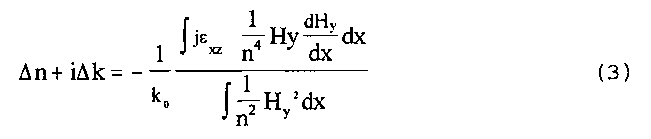
- Herein, Δn+iΔk shows the changed portion of the equivalent refractive index, K0 is the wave number of light in the vacuum, n is the refractive index of each layer of the waveguide, and Hy is a magnetic-field component of the transverse magnetic mode of the magnetic material formed on the waveguide.
- On the other side, the changed component of the equivalent refractive index to the light wave propagated in the - z direction is the same as to residual elements, except only that the sign of the term of εxz of the integration term at the right of expression (3) reverses. Therefore, the equivalent refractive index will differ between the travelling wave and the returning wave. By positively using the change in the equivalent refractive index of the nonreciprocity due to the magneto-optic effect, the energy attenuation amount according to the energy transfer caused when the light wave propagates in the said waveguide, from the optical waveguide to the optical absorptive magnetic material layer, changes according to the direction of propagation, so that an optical waveguide isolator can be achieved. In this case, the incident signal light can be output with light amplification by assuming the optical waveguide structure to be a semiconductor optical amplifier structure so as to compensate the attenuation amount of the signal light caused as the signal light propagates in the waveguide, so that the isolation function can be achieved without attenuating the signal light.
- Next, the isolation ratio is explained. The isolation ratio IR can be shown by the following expressions.
- By using expression (2), the isolation ratio can be shown by difference 2Δk between the attenuation of the forward-propagating wave and the attenuation of the backward propagating wave. This is shown by expression (5)
- Here, L is the length of the device. It was confirmed to be possible to obtain an isolation ratio of 40dB in a length of the device of about 2.0 mm since the optical waveguide isolator explained by the embodiment described later was simulated.
- In a preferable embodiment of the optical waveguide isolator according to the present invention, the first light wave is a signal light to be transmitted along a transmission system, and the second light wave is the return light propagated in the direction opposite to the signal light. According to such a construction, the signal light to be transmitted is not so attenuated, and the return light such as reflected light and the scattered light caused in transmission path can be greatly attenuated.
- In another embodiment of the optical waveguide isolator according to the present invention, the optical absorption magnetic material layer is constituted by magnetic material magnetized so as to have the magnetic-field component in the direction corresponding to the vibrating direction of a magnetic vector of the first light wave propagating on the waveguide. To obtain the nonreciprocity according to the magneto-optical effect, the direction of the external magnetic field should be made to correspond to the vibrating direction of the magnetic vector of the light wave having various modes propagating on the waveguide; for example, the magnetic material layer is formed in the case of the transverse magnetic mode light along the plane parallel to the substrate, so that the nonreciprocity according to the magnetoptical effect can be achieved by magnetizing the magnetic material layer in a direction orthogonal to the propagating direction of the light wave.
- As optical absorption magnetic material which causes the magneto-optical effect, ferromagnetic materials of nickel, iron, and cobalt, etc. and various magnetic materials such as yttrium iron garnet (YIG) can be used.
- According to a suitable embodiment of the optical waveguide isolator of the present invention, this substrate is a semiconductor substrate, and the core layer and first and second cladding layers are likewise constituted of semiconductor material. According to such a constitution, the optical waveguide isolator can be formed on the same semiconductor substrate with a semiconductor laser by using the usual semiconductor manufacturing technology.
- In another embodiment of the optical waveguide isolator according to the present invention, there is provided an optical waveguide isolator comprising a semiconductive light amplifier structure including a semiconductor substrate of a first conductivity type having a surface of a layer to be formed, a first cladding layer of the first conductivity type formed on the substrate, an active layer formed on the first cladding layer, a second cladding layer of the second conductivity type opposite to the first conductivity type, formed on the active layer, a first electrode formed on the surface of the semi-conductor substrate opposite to the surface to be formed as a layer, and a second electrode formed on the second cladding layer; the first cladding layer, the active layer, and the second cladding layer constitute an optical waveguide, the second electrode includes a light-absorptive magnetic material layer magnetized so as to have a magnetic-field component in the direction corresponding to the vibrating direction of the magnetic vector of the light wave propagating in the waveguide, the optical waveguide and the magnetic material layer of the second electrode constitute an optical waveguide structure, and the waveguide structure body has a nonreciprocity optical characteristic such that the effective refractive index of the optical waveguide for the light wave propagated changes according to the magneto-optical effect of the light-absorptive magnetic material layer according to the direction of propagation. By the effective refractive index change in the nonreciprocity, the attenuation of the first light wave that propagates through the optical waveguide in the first direction caused when the said waveguide is illuminated decreases less than the attenuation of the second light wave propagating in the second direction, opposite to the first direction. If the optical waveguide isolator is constituted as a semiconductor optical amplifier, the incident signal light can be amplified by adjusting the output voltage in the DC bias source connected between the first electrode and the second electrode and can emanate as a signal light with the same energy level as the energy level at the incident time.
- In another embodiment of the optical waveguide isolator having the light amplifier structure, one electrode of the light amplifier structure has a nickel layer and a gold layer which are magnetized in the direction corresponding to the vibrating direction of a magnetic vector of the first light wave. In this embodiment, there is the advantage that the electrode of the light amplifier can be co-used as an optical absorptive magnetic material layer.
- For a better understanding of the invention embodiments of it will now be described, by way of example, with reference to the accompanying drawings, in which:
- Fig. 1 is a diagrammatic sectional view showing the constitution of one embodiment of an optical isolator according to the present invention.
-
- Fig. 1 is a diagrammatic cross-sectional view showing the constitution of an optical waveguide isolator in accordance with the present invention. This embodiment explains the optical waveguide isolator having a semiconductor optical amplifier structure for amplifying and emitting incident light. In Fig. 1, the light wave is propagated in the z direction, and the semiconductor layer structure is formed along the x direction by y-z plane layers stacked in the x-direction. A substrate 1 of InP of n type is prepared, and the semiconductor layer structure is formed on a layer forming surface 1a of the substrate.
- The substrate 1 has a thickness of 100µm, and the high impurity concentration is assumed to be 1x10¹⁸ atoms/cm3 for example. For example, sulphur can be used to provide n-type impurities.
- A
first cladding layer 2 of n-type InP is deposited on the substrate 1 of InP. Thefirst cladding layer 2 has a thickness of 200 nm and a refractive index of 3.16, and the high impurity concentration is assumed to belx 1017 atoms/cm3. An undopedfirst guide layer 3 of InGaAsP is formed on thefirst cladding layer 2. The thickness of thefirst guide layer 3 is, for example, 120 nm, and the refractive index is 3.37. - An undoped
active layer 4 of InGaAsP is formed On thefirst guide layer 3. Theactive layer 4 has a thickness of 100 nm and refractive index of 3.4132. For example, in this embodiment, the active layer of monolayer structure is used, but a multiple quantum well structure of InGaAs and InGaAsP can be used. An undopedsecond guide layer 5 of InGaAsP is formed on theactive layer 4. Thesecond guide layer 5 has a thickness of 120 nm and a refractive index of 3.37. - A
second cladding layer 6 of p-type InP is deposited on thesecond guide layer 5. The second cladding layer has a thickness of 300 nm and a refractive index of 3.16, and its impurity concentration is 1x10¹⁷ atoms/cm3 . Acap layer 7 of p-type InGaAs is formed on thesecond cladding layer 6. Thecap layer 7 has a thickness of 30 nm, and its impurity concentration is 1x10¹⁹ atoms/cm3. - A
first electrode 8 is formed on thecap layer 7. Thefirst electrode 8 is formed by anickel layer 8a 50 nm in thickness and agold layer 8b 100 nm in thickness formed on thenickel layer 8a. Thenickel layer 8a constitutes anupper electrode 8 together with thegold layer 8b, and functions as an optical absorption magnetic material layer which exhibits a magneto-optical effect for the light wave propagating waveguide. Alower electrode 9 is formed on the other side of the substrate 1 opposite to the layer-forming surface la. The lower electrode is formed by atitanium layer 9a 50 nm in thickness and agold layer 9b 100 nm in thickness. ADC bias source 10 is connected between theupper electrode 8 and thelower electrode 9, so that the incident light wave is amplified to a level more than the original energy level thereof and emanates therefrom. - The optical waveguide isolator functions as a semiconductor optical amplifier and as a single optical waveguide structure. That is, the
active layer 4 and the first and second guide layers 3 and 5 formed on both sides thereof constitute a core layer of the optical waveguide, thefirst cladding layer 2 constitutes a cladding layer formed on the one side of the optical waveguide, thesecond cladding layer 6 andcap layer 7 form a cladding layer formed on the other side of the optical waveguide, and thenickel layer 8a constitutes an optical absorption magnetic material layer, so that an optical waveguide is constituted by the core layer and the first and second cladding layer, and an optically absorptive magnetic material layer is constituted by thenickel layer 8a, thereby constituting a single optical waveguide structure. In this case, the waveguide-type optical waveguide isolator, having substantially the same structure as the semiconductor laser, can be integrated on the same semiconductor substrate. - It is necessary that the optical waveguide isolator according to the present invention has an asymmetrical structure with regard to the light wave propagating in the waveguide. In the embodiment shown in Fig. 1, it can be considered that the y direction extends to infinity. On the other hand, the optically absorptive magnetic material layer is formed only on one side of the substrate about the x direction, so that an asymmetrical structure is secured in the x direction.
- The
second cladding layer 6 has an important function in defining the distance between the core layer and the optical absorptive magnetic material layer of the optical waveguide. The thickness of thesecond cladding layer 6 defines the energy amount which begins to exude on the light absorptivemagnetic material layer 8a side of the light wave propagating on the waveguide structure, that is, the amount that the evanescent light of the propagated light wave reaches the light absorptive magnetic material layer; it also defines the strength according to the magneto-optical effect of the propagated light wave to the optical absorptive magnetic material layer. Therefore, the thickness of thesecond cladding layer 6 is appropriately set in consideration of the wavelength of the light wave propagating on the waveguide and the usage as an optical waveguide isolator. - Next, the magnetizing direction of the optical absorptive
magnetic material layer 8a is explained. The transverse magnetic mode wave propagated in the z direction of Fig. l(from left to right) is taken as the signal light. In this case, the magnetic vector of the transverse magnetic mode wave vibrates in the y direction. Therefore, themagnetic material layer 8a is formed to be extended along the y direction, and magnetized so as to turn from the interior side of space to the frontward side. By magnetizing the optical absorptive magnetic material layer in such a direction, the attenuation of the signal light propagating in the z direction is minimized, while the attenuation of the reflected wave and the scattered light propagated in the opposite direction (the -z direction) can be maximized, and thus a large isolation ratio can be obtained. The magnetizing direction of the magnetic material layer need not accurately correspond to the direction of the magnetic vector of the light wave propagating the waveguide, and thus the desired performance can be obtained by only magnetizing the magnetic material layer so as to have a magnetic component in the direction corresponding to the direction of the magnetic vector. - Moreover, the vibrating direction of the magnetic vector of the transverse electric mode wave is the x direction in Fig. 1, so that in the case of the waveguide propagating the transverse electric mode wave, the optically absorptive magnetic material layer, extending in a direction which is substantially orthogonal to the layer-forming surface 1a of the substrate 1, is formed on the side of the waveguide structure, and the magneto-optical effect of the magnetic material layer can be used by magnetizing the optically absorptive magnetic material layer in the x direction.
- Next, the operation of the optical waveguide isolator, when the isolator shown in Fig. 1 is used as an optical waveguide isolator having light amplification operation, is explained. Assume that the signal light propagates in the + z direction (from the left side to the right side on the plane), and the return light to be attenuated propagates in the opposite (-z) direction. The optical waveguide isolator causes a strong attenuation operation for the return light and has a weak attenuation operation about the signal light. Therefore, the optical waveguide isolator performs optical amplification in such a manner that the attenuation level may at least become 0 dB for the incident signal light and the thus amplified light is emitted. The optical amplification rate is controlled by adjusting the voltage level of the
DC bias source 10. As a result, the energy level of the return light can be greatly attenuated without decreasing the energy level of the signal light to be propagated. - The present invention is not limited to the above described embodiment, and various modifications and changes can be performed. For example, the compound semiconductor materials of the InP system is used in the above described embodiment, but, for example, GaAs-system semiconductor material and GaN-system semiconductor material can be used. When GaAs-system semiconductor material is used, GaAs is used as a material of the core and A1GaAs can be used as a material of the cladding layer. Moreover, when GaN-system semiconductor material is used, InGaN is used as a material of the core and GaN can be used as a material of the cladding layer.
Claims (13)
- An optical isolator including a semiconductor substrate (1) of a first conductivity type having a surface (1a) for a layer to be formed thereon, a first cladding layer (2) of the first conductivity type formed on the substrate, an active layer (4) formed between the first cladding layer and a second cladding layer (6) of the second conductivity type, a first electrode (9) formed on the surface of the semiconductor substrate opposite to the layer-forming surface, and a second electrode (8) formed on the opposite side of the second cladding layer to the active layer (6), the first and the second cladding layers and the active layer (4) forming an optical waveguide in which a light wave propagates, the isolator further including a light absorbing magnetic material layer (8a) having a light absorption function for the light wave propagating through the optical waveguide, the magnetic material layer (8a) being magnetized so as to have the magnetic-field component in the direction which corresponds to the direction in which the magnetic vector of the light wave vibrates, the waveguide having a nonreciprocal optical characteristic such that the effective refractive index of the optical waveguide changes for the light wave according to the direction of propagation by virtue of the magneto-optical effect of the light-absorptive magnetic material layer (8a).
- An optical isolator as claimed in claim 1, wherein a first light wave is a signal light to be transmitted along a transmission system, and a second light wave is the return light propagated in the direction opposite to the signal light.
- An optical isolator as claimed in claim 2, wherein the signal light is a transverse magnetic mode wave, the magnetic-field component lying in the direction formed by the optical absorptive magnetic material layer (8a) in parallel to the layer-forming surface of the substrate and corresponding to the direction the magnetic vector of the signal light.
- An optical isolator as claimed in claim 2, wherein the signal light is a transverse electric mode wave and the light absorption magnetic material layer (8a) is formed substantially orthogonal to the layer-forming surface of the substrate, and has the magnetic-field component direction corresponding to the direction of the magnetic vector of the signal light.
- An optical isolator as claimed in any preceding claim, wherein the magnetic material is selected from magnetic materials of nickel, iron, cobalt or yttrium iron garnet (YIG).
- An optical isolator according to any of the preceding claims, wherein the second electrode (8) includes the light absorptive magnetic material layer (8a) and the optical waveguide and the magnetic material layer of the first electrode (8) constitute an optical waveguide structure.
- An optical isolator as claimed in claim 6, wherein the second electrode (8) has a nickel layer and a gold layer which are magnetized in the direction corresponding to the vibrating direction of the magnetic vector of the light wave.
- An optical system comprising an isolator as claimed in any of the preceding claims, further comprising a DC bias source (10) connected between the first electrode (8) and the second electrode (9), thereby performing light amplification so as to compensate for attenuation of the first light wave.
- An optical system, as claimed in claim 7, wherein the first light wave is signal light for optical amplification and the optical absorptive magnetic material layer (8a) is magnetized so as to have the magnetic-field component in the direction corresponding to the vibrating direction of the magnetic vector of the signal light.
- An optical isolator as claimed in any of the preceding claims, wherein the semiconductor substrate (1) is made of InP, the first and second cladding layers (2,6) are of InP, and the active layer is made of InGaAsP.
- An optical isolator as claimed in claim 10, wherein the first conductivity type is n type, and the second conductivity type is p type.
- An optical isolator as claimed in any of the preceding claims further comprising a guide layer (3,5) situated between the active layer (4) and each cladding layer (2,6).
- An optical isolator as claimed in any of the preceding claims further comprising a cap layer (7) between the second cladding layer (6) and the first electrode (8).
Applications Claiming Priority (2)
| Application Number | Priority Date | Filing Date | Title |
|---|---|---|---|
| JP7574699 | 1999-03-19 | ||
| JP11075746A JP3054707B1 (en) | 1999-03-19 | 1999-03-19 | Optical isolator |
Publications (3)
| Publication Number | Publication Date |
|---|---|
| EP1039330A2 true EP1039330A2 (en) | 2000-09-27 |
| EP1039330A3 EP1039330A3 (en) | 2001-02-21 |
| EP1039330B1 EP1039330B1 (en) | 2008-05-28 |
Family
ID=13585157
Family Applications (1)
| Application Number | Title | Priority Date | Filing Date |
|---|---|---|---|
| EP00302255A Expired - Lifetime EP1039330B1 (en) | 1999-03-19 | 2000-03-20 | Optical waveguide isolator |
Country Status (5)
| Country | Link |
|---|---|
| US (1) | US6208795B1 (en) |
| EP (1) | EP1039330B1 (en) |
| JP (1) | JP3054707B1 (en) |
| CA (1) | CA2300787C (en) |
| DE (1) | DE60038998D1 (en) |
Cited By (3)
| Publication number | Priority date | Publication date | Assignee | Title |
|---|---|---|---|---|
| EP1742313A1 (en) * | 2005-07-08 | 2007-01-10 | Alcatel | Optical device with integrated semiconductor laser and optical isolator |
| EP1719006A4 (en) * | 2004-02-12 | 2007-07-04 | Panorama Labs Pty Ltd | Apparatus, method, and computer program product for structured waveguide including performance-enhancing bounding region |
| WO2013057138A1 (en) * | 2011-10-20 | 2013-04-25 | Alcatel Lucent | Integrated optical structure comprising an optical isolator |
Families Citing this family (36)
| Publication number | Priority date | Publication date | Assignee | Title |
|---|---|---|---|---|
| JP3038383B1 (en) * | 1999-06-08 | 2000-05-08 | 東京大学長 | Optical device |
| WO2003032021A2 (en) | 2001-10-09 | 2003-04-17 | Infinera Corporation | TRANSMITTER PHOTONIC INTEGRATED CIRCUITS (TxPIC) AND OPTICAL TRANSPORT NETWORKS EMPLOYING TxPICs |
| JP2003185985A (en) * | 2001-12-14 | 2003-07-03 | Fujitsu Ltd | Optical circuit device and method of manufacturing the same |
| US6760496B2 (en) * | 2002-01-31 | 2004-07-06 | Photodigm, Inc. | Inline ferromagnetic-composite isolator and method |
| US7162113B2 (en) * | 2002-10-08 | 2007-01-09 | Infinera Corporation | Deployment of electro-optic amplitude varying elements (AVEs) and electro-optic multi-functional elements (MFEs) in photonic integrated circuits (PICs) |
| EP1813974B1 (en) * | 2003-03-31 | 2019-02-27 | Nippon Telegraph And Telephone Corporation | Integrated optical waveguide |
| US7065265B2 (en) * | 2003-05-12 | 2006-06-20 | Photodigm, Inc. | Ferromagnetic-semiconductor composite isolator and method |
| US7224854B2 (en) * | 2004-02-12 | 2007-05-29 | Panorama Labs Pty. Ltd. | System, method, and computer program product for structured waveguide including polarizer region |
| US20050180676A1 (en) * | 2004-02-12 | 2005-08-18 | Panorama Flat Ltd. | Faraday structured waveguide modulator |
| US7099547B2 (en) * | 2004-02-12 | 2006-08-29 | Panorama Labs Pty Ltd | Apparatus, method, and computer program product for structured waveguide transport using microbubbles |
| US20050185877A1 (en) * | 2004-02-12 | 2005-08-25 | Panorama Flat Ltd. | Apparatus, Method, and Computer Program Product For Structured Waveguide Switching Matrix |
| US20050201651A1 (en) * | 2004-02-12 | 2005-09-15 | Panorama Flat Ltd. | Apparatus, method, and computer program product for integrated influencer element |
| US7254287B2 (en) * | 2004-02-12 | 2007-08-07 | Panorama Labs, Pty Ltd. | Apparatus, method, and computer program product for transverse waveguided display system |
| US20060056792A1 (en) * | 2004-02-12 | 2006-03-16 | Panorama Flat Ltd. | System, method, and computer program product for structured waveguide including intra/inter contacting regions |
| US20060056793A1 (en) * | 2004-02-12 | 2006-03-16 | Panorama Flat Ltd. | System, method, and computer program product for structured waveguide including nonlinear effects |
| US20060056794A1 (en) * | 2004-02-12 | 2006-03-16 | Panorama Flat Ltd. | System, method, and computer program product for componentized displays using structured waveguides |
| US20050180723A1 (en) * | 2004-02-12 | 2005-08-18 | Panorama Flat Ltd. | Apparatus, method, and computer program product for structured waveguide including holding bounding region |
| US20050201654A1 (en) * | 2004-02-12 | 2005-09-15 | Panorama Flat Ltd. | Apparatus, method, and computer program product for substrated waveguided display system |
| US20050201679A1 (en) * | 2004-02-12 | 2005-09-15 | Panorama Flat Ltd. | System, method, and computer program product for structured waveguide including modified output regions |
| US20050180672A1 (en) * | 2004-02-12 | 2005-08-18 | Panorama Flat Ltd. | Apparatus, Method, and Computer Program Product For Multicolor Structured Waveguide |
| US20050180722A1 (en) * | 2004-02-12 | 2005-08-18 | Panorama Flat Ltd. | Apparatus, method, and computer program product for structured waveguide transport |
| US20050201705A1 (en) * | 2004-02-12 | 2005-09-15 | Panorama Flat Ltd. | Apparatus, method, and computer program product for structured waveguide including recursion zone |
| US20050180674A1 (en) * | 2004-02-12 | 2005-08-18 | Panorama Flat Ltd. | Faraday structured waveguide display |
| US20050201698A1 (en) * | 2004-02-12 | 2005-09-15 | Panorama Flat Ltd. | System, method, and computer program product for faceplate for structured waveguide system |
| JP2007140333A (en) * | 2005-11-22 | 2007-06-07 | Fujitsu Ltd | Optical element, optical element manufacturing method, and optical element driving method |
| JP5142100B2 (en) * | 2007-12-05 | 2013-02-13 | 公立大学法人大阪府立大学 | Light deflection method and apparatus |
| JP4807404B2 (en) * | 2008-11-18 | 2011-11-02 | 国立大学法人東京農工大学 | Integrated optical isolator and manufacturing method thereof |
| JP5393271B2 (en) | 2009-06-09 | 2014-01-22 | 信越化学工業株式会社 | Oxides and magneto-optical devices |
| JP5762715B2 (en) | 2010-10-06 | 2015-08-12 | 信越化学工業株式会社 | Magneto-optic material, Faraday rotator, and optical isolator |
| DE202011107213U1 (en) | 2011-10-27 | 2011-12-16 | Rudi Danz | Optical isolators with spectral conversion of light and generation of laser radiation |
| CA2918508C (en) | 2013-07-19 | 2020-12-08 | Shin-Etsu Chemical Co., Ltd. | Magneto-optical material, method for producing same and magneto-optical device |
| TWI634093B (en) | 2013-09-12 | 2018-09-01 | 信越化學工業股份有限公司 | Magneto-optical materials and magneto-optical devices |
| JP6465202B2 (en) | 2015-03-11 | 2019-02-06 | 信越化学工業株式会社 | Magneto-optical material, manufacturing method thereof, and magneto-optical device |
| CN105549154B (en) * | 2016-03-03 | 2019-05-10 | 电子科技大学 | A unidirectional magnetized semiconductor waveguide integrated multimode interference magneto-optical isolator |
| CN108107507B (en) * | 2017-12-19 | 2019-12-10 | 电子科技大学 | A kind of MMI type magneto-optical isolator and preparation method thereof |
| CN115933062B (en) * | 2022-12-23 | 2025-04-11 | 南开大学 | A fully polarized optical isolator |
Family Cites Families (5)
| Publication number | Priority date | Publication date | Assignee | Title |
|---|---|---|---|---|
| JPH0718964B2 (en) * | 1987-06-29 | 1995-03-06 | 日本電信電話株式会社 | Integrated optical device and manufacturing method thereof |
| US5747862A (en) * | 1992-09-25 | 1998-05-05 | Katsumi Kishino | Spin-polarized electron emitter having semiconductor opto-electronic layer with split valence band and reflecting mirror |
| DE69228422T2 (en) * | 1992-11-24 | 1999-09-30 | International Business Machines Corp., Armonk | Optical isolator for waveguides |
| JP3495066B2 (en) | 1993-10-07 | 2004-02-09 | 京セラ株式会社 | Optical fiber type non-reciprocal device |
| JP2879433B2 (en) * | 1997-01-16 | 1999-04-05 | 工業技術院長 | Semiconductor magneto-optical materials |
-
1999
- 1999-03-19 JP JP11075746A patent/JP3054707B1/en not_active Expired - Lifetime
-
2000
- 2000-03-16 US US09/527,022 patent/US6208795B1/en not_active Expired - Fee Related
- 2000-03-17 CA CA002300787A patent/CA2300787C/en not_active Expired - Fee Related
- 2000-03-20 DE DE60038998T patent/DE60038998D1/en not_active Expired - Lifetime
- 2000-03-20 EP EP00302255A patent/EP1039330B1/en not_active Expired - Lifetime
Non-Patent Citations (2)
| Title |
|---|
| HAMMER J M ET AL: "POLYCRYSTALLINE-METAL-FERROMAGNETIC OPTICAL WAVEGUIDE ISOLATOR (POWI) FOR MONOLITHIC-INTEGRATION WITH DIODE-LASER DEVICES" IEEE PHOTONICS TECHNOLOGY LETTERS,US,IEEE INC. NEW YORK, vol. 9, no. 5, 1 May 1997 (1997-05-01), pages 631-633, XP000677344 ISSN: 1041-1135 * |
| TAKENAKA MITSURU ET AL: "Proposal of a novel semiconductor optical waveguide isolator" PROCEEDINGS OF THE 1999 11TH INTERNATIONAL CONFERENCE ON INDIUM PHOSPHIDE AND RELATED MATERIALS (IPRM);DAVOS, SWITZ MAY 16-MAY 20 1999, 1999, pages 289-292, XP000974917 Conf Proc Int Conf Indium Phosphide and Relat Mater;Conference Proceedings - International Conference on Indium Phosphide and Related Materials 1999 IEEE, Piscataway, NJ, USA * |
Cited By (9)
| Publication number | Priority date | Publication date | Assignee | Title |
|---|---|---|---|---|
| EP1719006A4 (en) * | 2004-02-12 | 2007-07-04 | Panorama Labs Pty Ltd | Apparatus, method, and computer program product for structured waveguide including performance-enhancing bounding region |
| EP1742313A1 (en) * | 2005-07-08 | 2007-01-10 | Alcatel | Optical device with integrated semiconductor laser and optical isolator |
| FR2888410A1 (en) * | 2005-07-08 | 2007-01-12 | Alcatel Sa | OPTICAL DEVICE WITH INTEGRATED SEMICONDUCTOR LASER SOURCE AND OPTICAL ISOLATOR |
| CN100414791C (en) * | 2005-07-08 | 2008-08-27 | 阿尔卡特公司 | Optical device with integrated semiconductor laser source and integrated optical isolator |
| WO2013057138A1 (en) * | 2011-10-20 | 2013-04-25 | Alcatel Lucent | Integrated optical structure comprising an optical isolator |
| FR2981803A1 (en) * | 2011-10-20 | 2013-04-26 | Alcatel Lucent | INTEGRATED OPTICAL STRUCTURE COMPRISING AN OPTICAL ISOLATOR |
| CN103891068A (en) * | 2011-10-20 | 2014-06-25 | 阿尔卡特朗讯 | Integrated Optical Architecture Including Optical Isolators |
| TWI491952B (en) * | 2011-10-20 | 2015-07-11 | Alcatel Lucent | Integrated optical structure comprising an optical isolator |
| US9106046B2 (en) | 2011-10-20 | 2015-08-11 | Alcatel Lucent | Integrated optical structure comprising an optical isolator |
Also Published As
| Publication number | Publication date |
|---|---|
| CA2300787A1 (en) | 2000-09-19 |
| JP2000266947A (en) | 2000-09-29 |
| EP1039330A3 (en) | 2001-02-21 |
| CA2300787C (en) | 2002-12-31 |
| EP1039330B1 (en) | 2008-05-28 |
| JP3054707B1 (en) | 2000-06-19 |
| US6208795B1 (en) | 2001-03-27 |
| DE60038998D1 (en) | 2008-07-10 |
Similar Documents
| Publication | Publication Date | Title |
|---|---|---|
| EP1039330B1 (en) | Optical waveguide isolator | |
| CN1869748B (en) | Integratable Optical Isolator with Mach-Zehnder Interferometer Structure | |
| US8396337B2 (en) | Ring resonator based optical isolator and circulator | |
| US7065265B2 (en) | Ferromagnetic-semiconductor composite isolator and method | |
| US5598492A (en) | Metal-ferromagnetic optical waveguide isolator | |
| US20040223719A1 (en) | Magnetically active semiconductor waveguides for optoelectronic integration | |
| Zayets et al. | Complete magneto-optical waveguide mode conversion in Cd1− xMnxTe waveguide on GaAs substrate | |
| US12248207B2 (en) | Isolator, method of manufacturing isolator, electromagnetic wave transmitter, and light transmitter | |
| US4952017A (en) | Polarization independent semiconductor optical amplifier | |
| US8750666B2 (en) | Optical device using a plasmonic waveguide, and optical isolator | |
| EP2746839A1 (en) | Optical isolator | |
| JP2719187B2 (en) | Optical waveguide and optical isolator using the same | |
| Shimizu et al. | Plasmonic isolator for photonic integrated circuits | |
| EP3001241A1 (en) | Optoisolator | |
| US3860325A (en) | Electric field displacing type optical isolator | |
| CN111856791A (en) | Silicon-based magneto-optical isolator based on mode filter and preparation method | |
| JP4171831B2 (en) | Optical nonreciprocal device with silicon waveguide layer | |
| US6760496B2 (en) | Inline ferromagnetic-composite isolator and method | |
| US4047801A (en) | Optical wave guide having distributed gyrotropy | |
| Chi et al. | Nonlinear Y-junction coupler | |
| JPH0561002A (en) | Waveguide optical isolator and optical circulator | |
| Guo et al. | Magneto-optical semiconductor waveguides for integrated isolators | |
| Kuwahara et al. | An optical isolator for semiconductor lasers in the 0.8 μm range | |
| JP2546366B2 (en) | Semiconductor light emitting device | |
| Shimizu | Semiconductor optical isolators for integrated optics |
Legal Events
| Date | Code | Title | Description |
|---|---|---|---|
| PUAI | Public reference made under article 153(3) epc to a published international application that has entered the european phase |
Free format text: ORIGINAL CODE: 0009012 |
|
| 17P | Request for examination filed |
Effective date: 20000502 |
|
| AK | Designated contracting states |
Kind code of ref document: A2 Designated state(s): DE FR GB |
|
| AX | Request for extension of the european patent |
Free format text: AL;LT;LV;MK;RO;SI |
|
| PUAL | Search report despatched |
Free format text: ORIGINAL CODE: 0009013 |
|
| AK | Designated contracting states |
Kind code of ref document: A3 Designated state(s): AT BE CH CY DE DK ES FI FR GB GR IE IT LI LU MC NL PT SE |
|
| AX | Request for extension of the european patent |
Free format text: AL;LT;LV;MK;RO;SI |
|
| AKX | Designation fees paid |
Free format text: DE FR GB |
|
| 17Q | First examination report despatched |
Effective date: 20050207 |
|
| GRAP | Despatch of communication of intention to grant a patent |
Free format text: ORIGINAL CODE: EPIDOSNIGR1 |
|
| GRAS | Grant fee paid |
Free format text: ORIGINAL CODE: EPIDOSNIGR3 |
|
| GRAA | (expected) grant |
Free format text: ORIGINAL CODE: 0009210 |
|
| AK | Designated contracting states |
Kind code of ref document: B1 Designated state(s): DE FR GB |
|
| REG | Reference to a national code |
Ref country code: GB Ref legal event code: FG4D |
|
| REF | Corresponds to: |
Ref document number: 60038998 Country of ref document: DE Date of ref document: 20080710 Kind code of ref document: P |
|
| PLBE | No opposition filed within time limit |
Free format text: ORIGINAL CODE: 0009261 |
|
| STAA | Information on the status of an ep patent application or granted ep patent |
Free format text: STATUS: NO OPPOSITION FILED WITHIN TIME LIMIT |
|
| 26N | No opposition filed |
Effective date: 20090303 |
|
| PGFP | Annual fee paid to national office [announced via postgrant information from national office to epo] |
Ref country code: DE Payment date: 20110331 Year of fee payment: 12 |
|
| PGFP | Annual fee paid to national office [announced via postgrant information from national office to epo] |
Ref country code: FR Payment date: 20120326 Year of fee payment: 13 |
|
| PGFP | Annual fee paid to national office [announced via postgrant information from national office to epo] |
Ref country code: GB Payment date: 20120321 Year of fee payment: 13 |
|
| REG | Reference to a national code |
Ref country code: DE Ref legal event code: R119 Ref document number: 60038998 Country of ref document: DE Effective date: 20121002 |
|
| GBPC | Gb: european patent ceased through non-payment of renewal fee |
Effective date: 20130320 |
|
| REG | Reference to a national code |
Ref country code: FR Ref legal event code: ST Effective date: 20131129 |
|
| PG25 | Lapsed in a contracting state [announced via postgrant information from national office to epo] |
Ref country code: GB Free format text: LAPSE BECAUSE OF NON-PAYMENT OF DUE FEES Effective date: 20130320 Ref country code: FR Free format text: LAPSE BECAUSE OF NON-PAYMENT OF DUE FEES Effective date: 20130402 |
|
| PG25 | Lapsed in a contracting state [announced via postgrant information from national office to epo] |
Ref country code: DE Free format text: LAPSE BECAUSE OF NON-PAYMENT OF DUE FEES Effective date: 20121002 |