EP1038663A2 - Method of making an electronic module comprising a glass laminate - Google Patents
Method of making an electronic module comprising a glass laminate Download PDFInfo
- Publication number
- EP1038663A2 EP1038663A2 EP00200799A EP00200799A EP1038663A2 EP 1038663 A2 EP1038663 A2 EP 1038663A2 EP 00200799 A EP00200799 A EP 00200799A EP 00200799 A EP00200799 A EP 00200799A EP 1038663 A2 EP1038663 A2 EP 1038663A2
- Authority
- EP
- European Patent Office
- Prior art keywords
- glass
- panel
- substrates
- substrate
- modules
- Prior art date
- Legal status (The legal status is an assumption and is not a legal conclusion. Google has not performed a legal analysis and makes no representation as to the accuracy of the status listed.)
- Granted
Links
- 239000005340 laminated glass Substances 0.000 title claims description 11
- 238000004519 manufacturing process Methods 0.000 title claims description 10
- 239000000758 substrate Substances 0.000 claims abstract description 94
- 239000011521 glass Substances 0.000 claims abstract description 81
- 238000000034 method Methods 0.000 claims abstract description 56
- 239000002346 layers by function Substances 0.000 claims abstract description 37
- 238000000576 coating method Methods 0.000 claims description 15
- 238000010030 laminating Methods 0.000 claims description 9
- 238000005520 cutting process Methods 0.000 claims description 6
- 238000007639 printing Methods 0.000 claims description 5
- 230000008569 process Effects 0.000 claims description 5
- 239000010410 layer Substances 0.000 abstract description 62
- 239000011888 foil Substances 0.000 abstract description 21
- 239000004973 liquid crystal related substance Substances 0.000 abstract description 18
- 230000004888 barrier function Effects 0.000 abstract description 11
- 239000000203 mixture Substances 0.000 abstract description 10
- QVGXLLKOCUKJST-UHFFFAOYSA-N atomic oxygen Chemical compound [O] QVGXLLKOCUKJST-UHFFFAOYSA-N 0.000 abstract description 8
- 239000001301 oxygen Substances 0.000 abstract description 8
- 229910052760 oxygen Inorganic materials 0.000 abstract description 8
- XLYOFNOQVPJJNP-UHFFFAOYSA-N water Substances O XLYOFNOQVPJJNP-UHFFFAOYSA-N 0.000 abstract description 6
- 238000009792 diffusion process Methods 0.000 abstract description 4
- 230000015556 catabolic process Effects 0.000 abstract description 3
- 238000006731 degradation reaction Methods 0.000 abstract description 3
- 229920002457 flexible plastic Polymers 0.000 abstract description 2
- 125000006850 spacer group Chemical group 0.000 abstract description 2
- 229920003023 plastic Polymers 0.000 description 18
- 239000004033 plastic Substances 0.000 description 18
- 210000004027 cell Anatomy 0.000 description 14
- 239000011347 resin Substances 0.000 description 13
- 229920005989 resin Polymers 0.000 description 13
- 239000011248 coating agent Substances 0.000 description 11
- -1 poly(hydroxy amide ethers Chemical class 0.000 description 11
- 239000000463 material Substances 0.000 description 10
- 239000007789 gas Substances 0.000 description 9
- 239000012790 adhesive layer Substances 0.000 description 8
- VYPSYNLAJGMNEJ-UHFFFAOYSA-N Silicium dioxide Chemical compound O=[Si]=O VYPSYNLAJGMNEJ-UHFFFAOYSA-N 0.000 description 7
- 239000005388 borosilicate glass Substances 0.000 description 7
- 238000002438 flame photometric detection Methods 0.000 description 7
- 239000002650 laminated plastic Substances 0.000 description 7
- 238000003475 lamination Methods 0.000 description 6
- 239000010408 film Substances 0.000 description 5
- 239000011159 matrix material Substances 0.000 description 5
- 229920000642 polymer Polymers 0.000 description 5
- 238000004544 sputter deposition Methods 0.000 description 5
- DGAQECJNVWCQMB-PUAWFVPOSA-M Ilexoside XXIX Chemical compound C[C@@H]1CC[C@@]2(CC[C@@]3(C(=CC[C@H]4[C@]3(CC[C@@H]5[C@@]4(CC[C@@H](C5(C)C)OS(=O)(=O)[O-])C)C)[C@@H]2[C@]1(C)O)C)C(=O)O[C@H]6[C@@H]([C@H]([C@@H]([C@H](O6)CO)O)O)O.[Na+] DGAQECJNVWCQMB-PUAWFVPOSA-M 0.000 description 4
- OAICVXFJPJFONN-UHFFFAOYSA-N Phosphorus Chemical compound [P] OAICVXFJPJFONN-UHFFFAOYSA-N 0.000 description 4
- 239000000853 adhesive Substances 0.000 description 4
- 230000001070 adhesive effect Effects 0.000 description 4
- 239000003513 alkali Substances 0.000 description 4
- 229920001577 copolymer Polymers 0.000 description 4
- 239000005329 float glass Substances 0.000 description 4
- 229910052751 metal Inorganic materials 0.000 description 4
- 239000002184 metal Substances 0.000 description 4
- 229920000123 polythiophene Polymers 0.000 description 4
- 239000011734 sodium Substances 0.000 description 4
- 229910052708 sodium Inorganic materials 0.000 description 4
- 239000000243 solution Substances 0.000 description 4
- 239000000126 substance Substances 0.000 description 4
- 230000008901 benefit Effects 0.000 description 3
- 239000000919 ceramic Substances 0.000 description 3
- 238000005229 chemical vapour deposition Methods 0.000 description 3
- 239000005345 chemically strengthened glass Substances 0.000 description 3
- 238000002347 injection Methods 0.000 description 3
- 239000007924 injection Substances 0.000 description 3
- 238000000206 photolithography Methods 0.000 description 3
- 238000005240 physical vapour deposition Methods 0.000 description 3
- 239000002985 plastic film Substances 0.000 description 3
- 229920000553 poly(phenylenevinylene) Polymers 0.000 description 3
- 229920000178 Acrylic resin Polymers 0.000 description 2
- 239000004925 Acrylic resin Substances 0.000 description 2
- KAKZBPTYRLMSJV-UHFFFAOYSA-N Butadiene Chemical compound C=CC=C KAKZBPTYRLMSJV-UHFFFAOYSA-N 0.000 description 2
- 235000008733 Citrus aurantifolia Nutrition 0.000 description 2
- JOYRKODLDBILNP-UHFFFAOYSA-N Ethyl urethane Chemical compound CCOC(N)=O JOYRKODLDBILNP-UHFFFAOYSA-N 0.000 description 2
- 239000001828 Gelatine Substances 0.000 description 2
- PXHVJJICTQNCMI-UHFFFAOYSA-N Nickel Chemical compound [Ni] PXHVJJICTQNCMI-UHFFFAOYSA-N 0.000 description 2
- 239000004695 Polyether sulfone Substances 0.000 description 2
- 239000004698 Polyethylene Substances 0.000 description 2
- ZLMJMSJWJFRBEC-UHFFFAOYSA-N Potassium Chemical group [K] ZLMJMSJWJFRBEC-UHFFFAOYSA-N 0.000 description 2
- BQCADISMDOOEFD-UHFFFAOYSA-N Silver Chemical compound [Ag] BQCADISMDOOEFD-UHFFFAOYSA-N 0.000 description 2
- PPBRXRYQALVLMV-UHFFFAOYSA-N Styrene Chemical compound C=CC1=CC=CC=C1 PPBRXRYQALVLMV-UHFFFAOYSA-N 0.000 description 2
- 235000011941 Tilia x europaea Nutrition 0.000 description 2
- 238000005452 bending Methods 0.000 description 2
- 239000003795 chemical substances by application Substances 0.000 description 2
- 229910052681 coesite Inorganic materials 0.000 description 2
- 150000001875 compounds Chemical class 0.000 description 2
- 229910052906 cristobalite Inorganic materials 0.000 description 2
- 238000007766 curtain coating Methods 0.000 description 2
- 239000006185 dispersion Substances 0.000 description 2
- 238000010894 electron beam technology Methods 0.000 description 2
- 238000005516 engineering process Methods 0.000 description 2
- 239000003822 epoxy resin Substances 0.000 description 2
- OILFVDKXWWPVNO-UHFFFAOYSA-N ethyl n-phenoxycarbamate Chemical compound CCOC(=O)NOC1=CC=CC=C1 OILFVDKXWWPVNO-UHFFFAOYSA-N 0.000 description 2
- 229920000159 gelatin Polymers 0.000 description 2
- 235000019322 gelatine Nutrition 0.000 description 2
- 238000010438 heat treatment Methods 0.000 description 2
- 229910003437 indium oxide Inorganic materials 0.000 description 2
- RHZWSUVWRRXEJF-UHFFFAOYSA-N indium tin Chemical compound [In].[Sn] RHZWSUVWRRXEJF-UHFFFAOYSA-N 0.000 description 2
- PJXISJQVUVHSOJ-UHFFFAOYSA-N indium(iii) oxide Chemical compound [O-2].[O-2].[O-2].[In+3].[In+3] PJXISJQVUVHSOJ-UHFFFAOYSA-N 0.000 description 2
- 150000002500 ions Chemical class 0.000 description 2
- 239000004571 lime Substances 0.000 description 2
- 239000006060 molten glass Substances 0.000 description 2
- 239000012044 organic layer Substances 0.000 description 2
- 229920000647 polyepoxide Polymers 0.000 description 2
- 229920006393 polyether sulfone Polymers 0.000 description 2
- 229920000573 polyethylene Polymers 0.000 description 2
- 239000005020 polyethylene terephthalate Substances 0.000 description 2
- 229920000139 polyethylene terephthalate Polymers 0.000 description 2
- 229920001721 polyimide Polymers 0.000 description 2
- 229910052700 potassium Inorganic materials 0.000 description 2
- 239000011591 potassium Substances 0.000 description 2
- 238000011160 research Methods 0.000 description 2
- 239000000377 silicon dioxide Substances 0.000 description 2
- 229910052814 silicon oxide Inorganic materials 0.000 description 2
- 229910052709 silver Inorganic materials 0.000 description 2
- 239000004332 silver Substances 0.000 description 2
- 238000007767 slide coating Methods 0.000 description 2
- 229910052682 stishovite Inorganic materials 0.000 description 2
- 239000010409 thin film Substances 0.000 description 2
- 229910052905 tridymite Inorganic materials 0.000 description 2
- 239000013585 weight reducing agent Substances 0.000 description 2
- NGQSLSMAEVWNPU-YTEMWHBBSA-N 1,2-bis[(e)-2-phenylethenyl]benzene Chemical class C=1C=CC=CC=1/C=C/C1=CC=CC=C1\C=C\C1=CC=CC=C1 NGQSLSMAEVWNPU-YTEMWHBBSA-N 0.000 description 1
- GNLJOAHHAPACCT-UHFFFAOYSA-N 4-diethoxyphosphorylmorpholine Chemical compound CCOP(=O)(OCC)N1CCOCC1 GNLJOAHHAPACCT-UHFFFAOYSA-N 0.000 description 1
- NLHHRLWOUZZQLW-UHFFFAOYSA-N Acrylonitrile Chemical compound C=CC#N NLHHRLWOUZZQLW-UHFFFAOYSA-N 0.000 description 1
- DKPFZGUDAPQIHT-UHFFFAOYSA-N Butyl acetate Natural products CCCCOC(C)=O DKPFZGUDAPQIHT-UHFFFAOYSA-N 0.000 description 1
- 229920001747 Cellulose diacetate Polymers 0.000 description 1
- 229920002284 Cellulose triacetate Polymers 0.000 description 1
- 239000004593 Epoxy Substances 0.000 description 1
- WHXSMMKQMYFTQS-UHFFFAOYSA-N Lithium Chemical compound [Li] WHXSMMKQMYFTQS-UHFFFAOYSA-N 0.000 description 1
- HBBGRARXTFLTSG-UHFFFAOYSA-N Lithium ion Chemical compound [Li+] HBBGRARXTFLTSG-UHFFFAOYSA-N 0.000 description 1
- 241001082241 Lythrum hyssopifolia Species 0.000 description 1
- ZOKXTWBITQBERF-UHFFFAOYSA-N Molybdenum Chemical compound [Mo] ZOKXTWBITQBERF-UHFFFAOYSA-N 0.000 description 1
- KKCBUQHMOMHUOY-UHFFFAOYSA-N Na2O Inorganic materials [O-2].[Na+].[Na+] KKCBUQHMOMHUOY-UHFFFAOYSA-N 0.000 description 1
- 239000004696 Poly ether ether ketone Substances 0.000 description 1
- 229920012266 Poly(ether sulfone) PES Polymers 0.000 description 1
- 239000004721 Polyphenylene oxide Substances 0.000 description 1
- 239000004743 Polypropylene Substances 0.000 description 1
- NNLVGZFZQQXQNW-ADJNRHBOSA-N [(2r,3r,4s,5r,6s)-4,5-diacetyloxy-3-[(2s,3r,4s,5r,6r)-3,4,5-triacetyloxy-6-(acetyloxymethyl)oxan-2-yl]oxy-6-[(2r,3r,4s,5r,6s)-4,5,6-triacetyloxy-2-(acetyloxymethyl)oxan-3-yl]oxyoxan-2-yl]methyl acetate Chemical compound O([C@@H]1O[C@@H]([C@H]([C@H](OC(C)=O)[C@H]1OC(C)=O)O[C@H]1[C@@H]([C@@H](OC(C)=O)[C@H](OC(C)=O)[C@@H](COC(C)=O)O1)OC(C)=O)COC(=O)C)[C@@H]1[C@@H](COC(C)=O)O[C@@H](OC(C)=O)[C@H](OC(C)=O)[C@H]1OC(C)=O NNLVGZFZQQXQNW-ADJNRHBOSA-N 0.000 description 1
- 239000002253 acid Substances 0.000 description 1
- 239000002390 adhesive tape Substances 0.000 description 1
- 238000007754 air knife coating Methods 0.000 description 1
- 239000012670 alkaline solution Substances 0.000 description 1
- 239000007864 aqueous solution Substances 0.000 description 1
- 150000004982 aromatic amines Chemical class 0.000 description 1
- 238000010923 batch production Methods 0.000 description 1
- 238000007664 blowing Methods 0.000 description 1
- 239000003990 capacitor Substances 0.000 description 1
- 210000002421 cell wall Anatomy 0.000 description 1
- 239000012461 cellulose resin Substances 0.000 description 1
- 238000003426 chemical strengthening reaction Methods 0.000 description 1
- 229920001940 conductive polymer Polymers 0.000 description 1
- 238000011437 continuous method Methods 0.000 description 1
- 238000010924 continuous production Methods 0.000 description 1
- 238000001816 cooling Methods 0.000 description 1
- 230000032798 delamination Effects 0.000 description 1
- 230000001419 dependent effect Effects 0.000 description 1
- 238000000151 deposition Methods 0.000 description 1
- 230000008021 deposition Effects 0.000 description 1
- 238000011161 development Methods 0.000 description 1
- 238000003618 dip coating Methods 0.000 description 1
- 238000001035 drying Methods 0.000 description 1
- 239000008151 electrolyte solution Substances 0.000 description 1
- 229920006332 epoxy adhesive Polymers 0.000 description 1
- 238000007765 extrusion coating Methods 0.000 description 1
- 238000011049 filling Methods 0.000 description 1
- 239000010419 fine particle Substances 0.000 description 1
- 125000003983 fluorenyl group Chemical class C1(=CC=CC=2C3=CC=CC=C3CC12)* 0.000 description 1
- 150000002240 furans Chemical class 0.000 description 1
- 239000003365 glass fiber Substances 0.000 description 1
- 238000007756 gravure coating Methods 0.000 description 1
- 238000000227 grinding Methods 0.000 description 1
- 230000005283 ground state Effects 0.000 description 1
- FUZZWVXGSFPDMH-UHFFFAOYSA-N hexanoic acid Chemical compound CCCCCC(O)=O FUZZWVXGSFPDMH-UHFFFAOYSA-N 0.000 description 1
- 239000012943 hotmelt Substances 0.000 description 1
- 239000011810 insulating material Substances 0.000 description 1
- 238000005342 ion exchange Methods 0.000 description 1
- 229910000464 lead oxide Inorganic materials 0.000 description 1
- 239000007788 liquid Substances 0.000 description 1
- 229910052744 lithium Inorganic materials 0.000 description 1
- 229910001416 lithium ion Inorganic materials 0.000 description 1
- 229920002521 macromolecule Polymers 0.000 description 1
- CPLXHLVBOLITMK-UHFFFAOYSA-N magnesium oxide Inorganic materials [Mg]=O CPLXHLVBOLITMK-UHFFFAOYSA-N 0.000 description 1
- 239000000395 magnesium oxide Substances 0.000 description 1
- AXZKOIWUVFPNLO-UHFFFAOYSA-N magnesium;oxygen(2-) Chemical compound [O-2].[Mg+2] AXZKOIWUVFPNLO-UHFFFAOYSA-N 0.000 description 1
- 238000001755 magnetron sputter deposition Methods 0.000 description 1
- 238000002844 melting Methods 0.000 description 1
- 230000008018 melting Effects 0.000 description 1
- 229910052750 molybdenum Inorganic materials 0.000 description 1
- 239000011733 molybdenum Substances 0.000 description 1
- 229910052759 nickel Inorganic materials 0.000 description 1
- 229910052756 noble gas Inorganic materials 0.000 description 1
- 150000002835 noble gases Chemical class 0.000 description 1
- 238000007645 offset printing Methods 0.000 description 1
- 230000003287 optical effect Effects 0.000 description 1
- 239000012860 organic pigment Substances 0.000 description 1
- 239000003960 organic solvent Substances 0.000 description 1
- 230000003647 oxidation Effects 0.000 description 1
- 238000007254 oxidation reaction Methods 0.000 description 1
- YEXPOXQUZXUXJW-UHFFFAOYSA-N oxolead Chemical compound [Pb]=O YEXPOXQUZXUXJW-UHFFFAOYSA-N 0.000 description 1
- 230000035699 permeability Effects 0.000 description 1
- 229920006287 phenoxy resin Polymers 0.000 description 1
- 239000013034 phenoxy resin Substances 0.000 description 1
- 125000001997 phenyl group Chemical group [H]C1=C([H])C([H])=C(*)C([H])=C1[H] 0.000 description 1
- 229920006255 plastic film Polymers 0.000 description 1
- 229920001643 poly(ether ketone) Polymers 0.000 description 1
- 229920002492 poly(sulfone) Polymers 0.000 description 1
- 229920002037 poly(vinyl butyral) polymer Polymers 0.000 description 1
- 229920002239 polyacrylonitrile Polymers 0.000 description 1
- 239000004417 polycarbonate Substances 0.000 description 1
- 229920000515 polycarbonate Polymers 0.000 description 1
- 229920000570 polyether Polymers 0.000 description 1
- 229920002530 polyetherether ketone Polymers 0.000 description 1
- 229920013716 polyethylene resin Polymers 0.000 description 1
- 239000009719 polyimide resin Substances 0.000 description 1
- 229920001155 polypropylene Polymers 0.000 description 1
- 229920000128 polypyrrole Polymers 0.000 description 1
- 229920001296 polysiloxane Polymers 0.000 description 1
- 229920002451 polyvinyl alcohol Polymers 0.000 description 1
- 238000002360 preparation method Methods 0.000 description 1
- 150000003233 pyrroles Chemical class 0.000 description 1
- 238000001552 radio frequency sputter deposition Methods 0.000 description 1
- 230000009467 reduction Effects 0.000 description 1
- 230000027756 respiratory electron transport chain Effects 0.000 description 1
- 238000007763 reverse roll coating Methods 0.000 description 1
- 238000007650 screen-printing Methods 0.000 description 1
- 238000007789 sealing Methods 0.000 description 1
- 239000005361 soda-lime glass Substances 0.000 description 1
- 229910001415 sodium ion Inorganic materials 0.000 description 1
- 239000007787 solid Substances 0.000 description 1
- 239000002904 solvent Substances 0.000 description 1
- 238000004528 spin coating Methods 0.000 description 1
- 239000002344 surface layer Substances 0.000 description 1
- 230000003746 surface roughness Effects 0.000 description 1
- 238000007669 thermal treatment Methods 0.000 description 1
- 229920002803 thermoplastic polyurethane Polymers 0.000 description 1
- 229930192474 thiophene Natural products 0.000 description 1
- 150000003577 thiophenes Chemical class 0.000 description 1
- XOLBLPGZBRYERU-UHFFFAOYSA-N tin dioxide Chemical compound O=[Sn]=O XOLBLPGZBRYERU-UHFFFAOYSA-N 0.000 description 1
- 229910001887 tin oxide Inorganic materials 0.000 description 1
- 238000002834 transmittance Methods 0.000 description 1
- 239000012780 transparent material Substances 0.000 description 1
- 238000011282 treatment Methods 0.000 description 1
- 238000001429 visible spectrum Methods 0.000 description 1
Images
Classifications
-
- G—PHYSICS
- G02—OPTICS
- G02F—OPTICAL DEVICES OR ARRANGEMENTS FOR THE CONTROL OF LIGHT BY MODIFICATION OF THE OPTICAL PROPERTIES OF THE MEDIA OF THE ELEMENTS INVOLVED THEREIN; NON-LINEAR OPTICS; FREQUENCY-CHANGING OF LIGHT; OPTICAL LOGIC ELEMENTS; OPTICAL ANALOGUE/DIGITAL CONVERTERS
- G02F1/00—Devices or arrangements for the control of the intensity, colour, phase, polarisation or direction of light arriving from an independent light source, e.g. switching, gating or modulating; Non-linear optics
- G02F1/01—Devices or arrangements for the control of the intensity, colour, phase, polarisation or direction of light arriving from an independent light source, e.g. switching, gating or modulating; Non-linear optics for the control of the intensity, phase, polarisation or colour
- G02F1/13—Devices or arrangements for the control of the intensity, colour, phase, polarisation or direction of light arriving from an independent light source, e.g. switching, gating or modulating; Non-linear optics for the control of the intensity, phase, polarisation or colour based on liquid crystals, e.g. single liquid crystal display cells
- G02F1/133—Constructional arrangements; Operation of liquid crystal cells; Circuit arrangements
- G02F1/1333—Constructional arrangements; Manufacturing methods
- G02F1/133351—Manufacturing of individual cells out of a plurality of cells, e.g. by dicing
-
- B—PERFORMING OPERATIONS; TRANSPORTING
- B32—LAYERED PRODUCTS
- B32B—LAYERED PRODUCTS, i.e. PRODUCTS BUILT-UP OF STRATA OF FLAT OR NON-FLAT, e.g. CELLULAR OR HONEYCOMB, FORM
- B32B17/00—Layered products essentially comprising sheet glass, or glass, slag, or like fibres
- B32B17/06—Layered products essentially comprising sheet glass, or glass, slag, or like fibres comprising glass as the main or only constituent of a layer, next to another layer of a specific material
- B32B17/10—Layered products essentially comprising sheet glass, or glass, slag, or like fibres comprising glass as the main or only constituent of a layer, next to another layer of a specific material of synthetic resin
- B32B17/10005—Layered products essentially comprising sheet glass, or glass, slag, or like fibres comprising glass as the main or only constituent of a layer, next to another layer of a specific material of synthetic resin laminated safety glass or glazing
- B32B17/10009—Layered products essentially comprising sheet glass, or glass, slag, or like fibres comprising glass as the main or only constituent of a layer, next to another layer of a specific material of synthetic resin laminated safety glass or glazing characterized by the number, the constitution or treatment of glass sheets
- B32B17/10036—Layered products essentially comprising sheet glass, or glass, slag, or like fibres comprising glass as the main or only constituent of a layer, next to another layer of a specific material of synthetic resin laminated safety glass or glazing characterized by the number, the constitution or treatment of glass sheets comprising two outer glass sheets
-
- B—PERFORMING OPERATIONS; TRANSPORTING
- B32—LAYERED PRODUCTS
- B32B—LAYERED PRODUCTS, i.e. PRODUCTS BUILT-UP OF STRATA OF FLAT OR NON-FLAT, e.g. CELLULAR OR HONEYCOMB, FORM
- B32B17/00—Layered products essentially comprising sheet glass, or glass, slag, or like fibres
- B32B17/06—Layered products essentially comprising sheet glass, or glass, slag, or like fibres comprising glass as the main or only constituent of a layer, next to another layer of a specific material
- B32B17/10—Layered products essentially comprising sheet glass, or glass, slag, or like fibres comprising glass as the main or only constituent of a layer, next to another layer of a specific material of synthetic resin
- B32B17/10005—Layered products essentially comprising sheet glass, or glass, slag, or like fibres comprising glass as the main or only constituent of a layer, next to another layer of a specific material of synthetic resin laminated safety glass or glazing
- B32B17/10165—Functional features of the laminated safety glass or glazing
- B32B17/10174—Coatings of a metallic or dielectric material on a constituent layer of glass or polymer
-
- G—PHYSICS
- G02—OPTICS
- G02F—OPTICAL DEVICES OR ARRANGEMENTS FOR THE CONTROL OF LIGHT BY MODIFICATION OF THE OPTICAL PROPERTIES OF THE MEDIA OF THE ELEMENTS INVOLVED THEREIN; NON-LINEAR OPTICS; FREQUENCY-CHANGING OF LIGHT; OPTICAL LOGIC ELEMENTS; OPTICAL ANALOGUE/DIGITAL CONVERTERS
- G02F1/00—Devices or arrangements for the control of the intensity, colour, phase, polarisation or direction of light arriving from an independent light source, e.g. switching, gating or modulating; Non-linear optics
- G02F1/01—Devices or arrangements for the control of the intensity, colour, phase, polarisation or direction of light arriving from an independent light source, e.g. switching, gating or modulating; Non-linear optics for the control of the intensity, phase, polarisation or colour
- G02F1/13—Devices or arrangements for the control of the intensity, colour, phase, polarisation or direction of light arriving from an independent light source, e.g. switching, gating or modulating; Non-linear optics for the control of the intensity, phase, polarisation or colour based on liquid crystals, e.g. single liquid crystal display cells
- G02F1/133—Constructional arrangements; Operation of liquid crystal cells; Circuit arrangements
- G02F1/1333—Constructional arrangements; Manufacturing methods
- G02F1/133305—Flexible substrates, e.g. plastics, organic film
-
- G—PHYSICS
- G02—OPTICS
- G02F—OPTICAL DEVICES OR ARRANGEMENTS FOR THE CONTROL OF LIGHT BY MODIFICATION OF THE OPTICAL PROPERTIES OF THE MEDIA OF THE ELEMENTS INVOLVED THEREIN; NON-LINEAR OPTICS; FREQUENCY-CHANGING OF LIGHT; OPTICAL LOGIC ELEMENTS; OPTICAL ANALOGUE/DIGITAL CONVERTERS
- G02F1/00—Devices or arrangements for the control of the intensity, colour, phase, polarisation or direction of light arriving from an independent light source, e.g. switching, gating or modulating; Non-linear optics
- G02F1/01—Devices or arrangements for the control of the intensity, colour, phase, polarisation or direction of light arriving from an independent light source, e.g. switching, gating or modulating; Non-linear optics for the control of the intensity, phase, polarisation or colour
- G02F1/13—Devices or arrangements for the control of the intensity, colour, phase, polarisation or direction of light arriving from an independent light source, e.g. switching, gating or modulating; Non-linear optics for the control of the intensity, phase, polarisation or colour based on liquid crystals, e.g. single liquid crystal display cells
- G02F1/133—Constructional arrangements; Operation of liquid crystal cells; Circuit arrangements
- G02F1/1333—Constructional arrangements; Manufacturing methods
- G02F1/133302—Rigid substrates, e.g. inorganic substrates
-
- G—PHYSICS
- G02—OPTICS
- G02F—OPTICAL DEVICES OR ARRANGEMENTS FOR THE CONTROL OF LIGHT BY MODIFICATION OF THE OPTICAL PROPERTIES OF THE MEDIA OF THE ELEMENTS INVOLVED THEREIN; NON-LINEAR OPTICS; FREQUENCY-CHANGING OF LIGHT; OPTICAL LOGIC ELEMENTS; OPTICAL ANALOGUE/DIGITAL CONVERTERS
- G02F1/00—Devices or arrangements for the control of the intensity, colour, phase, polarisation or direction of light arriving from an independent light source, e.g. switching, gating or modulating; Non-linear optics
- G02F1/01—Devices or arrangements for the control of the intensity, colour, phase, polarisation or direction of light arriving from an independent light source, e.g. switching, gating or modulating; Non-linear optics for the control of the intensity, phase, polarisation or colour
- G02F1/13—Devices or arrangements for the control of the intensity, colour, phase, polarisation or direction of light arriving from an independent light source, e.g. switching, gating or modulating; Non-linear optics for the control of the intensity, phase, polarisation or colour based on liquid crystals, e.g. single liquid crystal display cells
- G02F1/133—Constructional arrangements; Operation of liquid crystal cells; Circuit arrangements
- G02F1/1333—Constructional arrangements; Manufacturing methods
- G02F1/133345—Insulating layers
-
- H—ELECTRICITY
- H10—SEMICONDUCTOR DEVICES; ELECTRIC SOLID-STATE DEVICES NOT OTHERWISE PROVIDED FOR
- H10K—ORGANIC ELECTRIC SOLID-STATE DEVICES
- H10K2102/00—Constructional details relating to the organic devices covered by this subclass
- H10K2102/301—Details of OLEDs
- H10K2102/311—Flexible OLED
-
- H—ELECTRICITY
- H10—SEMICONDUCTOR DEVICES; ELECTRIC SOLID-STATE DEVICES NOT OTHERWISE PROVIDED FOR
- H10K—ORGANIC ELECTRIC SOLID-STATE DEVICES
- H10K2102/00—Constructional details relating to the organic devices covered by this subclass
- H10K2102/301—Details of OLEDs
- H10K2102/351—Thickness
-
- H—ELECTRICITY
- H10—SEMICONDUCTOR DEVICES; ELECTRIC SOLID-STATE DEVICES NOT OTHERWISE PROVIDED FOR
- H10K—ORGANIC ELECTRIC SOLID-STATE DEVICES
- H10K71/00—Manufacture or treatment specially adapted for the organic devices covered by this subclass
- H10K71/851—Division of substrate
Definitions
- the present invention relates to a method for making an electric or electronic device such as a flat panel display, a light emitting diode or a photovoltaic cell. More specifically, the present invention relates to a method wherein a thin glass sheet is laminated to a substrate which is provided with one or more functional layers used in such electric or electronic devices, e.g. an electroconductive layer, a colour filter, a liquid crystal alignment layer, a phosphor layer, etc.
- LCDs Liquid crystal displays
- CTRs cathode ray tubes
- FPD flat panel display
- PDs plasma displays
- FEDs field emission displays
- OLEDs organic light-emitting displays
- PDs Being emissive displays, PDs, FEDs or OLEDs may provide a solution for two major problems associated with LCDs, i.e. the low viewing angle and low efficiency (typically, only a few percent of the incident light or backlight passes through an LCD to form a readable image).
- two substrates are being used for carrying functional layers, e.g. electroconductive layers for pixel addressing, colour filters, liquid crystal orientation or alignment layers in LCDs or phosphor layers in FEDs and PDs.
- a filling e.g. a liquid crystal compound (LCDs), a light-emitting substance (LEDs) or a plasma-forming gas (PDs).
- LCDs liquid crystal compound
- LEDs light-emitting substance
- PDs plasma-forming gas
- one or more foils can be laminated to the outer surface of the glass substrate.
- polarisor foils are necessary components which are laminated to the glass substrate.
- several other types of foils are widely used to improve the image quality, e.g. retardation film, reflection or anti-reflection foils, foils which improve the viewing angle, light dispersion foils, etc.
- the substrates used in such devices are typically glass plates having a thickness in the range from 0.7 to 1.1 mm. Due to the high specific weight of glass, the total weight of a display is mainly determined by the size and thickness of these glass plates.
- Weight reduction is important for mobile displays as well as for large stationary displays such as television sets and desktop computer displays. A further reduction of the thickness of the glass plates is however limited due to the high brittleness of such thin glass.
- plastic sheets are being used as a low-weight substrate of a FPD.
- the high strength and flexibility of plastics even enables the making of a flexible display.
- the flexibility of plastic substrates enables the use of continuous processes for applying a functional layer thereon, e.g. using a web or roll coater or by printing, while the coating on glass typically proceeds in a batch process (sheet by sheet).
- the liquid crystal composition and other functional layers, especially the electroconductive layers, present between such plastic substrates are not well protected from chemicals, oxygen, moisture, mechanical impact and other external influences and, as a result, the lifetime of such plastic-based devices is limited.
- plastics have a very low thermal and dimensional stability compared to glass, which are essential properties required for obtaining high quality displays.
- barrier layers which can be provided on plastic foils to reduce to diffusion of moisture and gases as described in e.g. US-P-4,950,551; US-P-5,589,252; and US-P-5,820,994.
- barrier layers are the so-called Organically Modified Ceramic layers, as described in Coating, no. 9/98, p.314 and 10/97, p.358, and the poly(hydroxy amide ethers) described in Macromolecules, vol.31, p.8281 (1998).
- WO99/21707 and WO99/21708 propose to use a laminate as substrate which comprises a glass layer, an adhesive layer and a plastic support.
- a laminate which comprises a glass layer, an adhesive layer and a plastic support.
- Such glass/plastic laminates combine the advantageous properties of glass and plastics.
- the glass protects the plastic substrate from scratches, moisture, solvents and gases, and improves the dimensional and thermal stability of the substrate.
- a thin glass e.g. a glass as described in EP-A-716339
- the glass/plastic laminate is flexible and can be wound around a core, enabling the use of web or roll coating methods.
- the devices which are obtained using such glass/plastic laminates as substrate are characterised by a lower weight than full-glass based devices and by a lower probability of breakage of the substrate during handling or dropping the device.
- the functional layers needed in electric or electronic devices such as FPDs, photovoltaic cells and LEDs are typically applied on the substrate using methods such as sputtering, photolithography, physical vapour deposition, chemical vapour deposition, etc.
- the substrate is subjected to high temperature and/or chemical treatments with various organic solvents and acid or alkaline solutions.
- the glass/plastic laminates described above may curl or even break due to the different thermal expansion coefficient of glass and plastic or the adhesive layer may be degraded so that the bond between the glass and plastic is destroyed.
- Another problem is associated with the cutting of glass/plastic laminates.
- FPDs such as LCDs are being manufactured from substrates having a large size up to 500x400 or even 650x550 mm. After assembling the panel, the substrates are cut so as to obtain from two to nine modules (displays cells) from one panel.
- Using glass/plastic laminates as substrate requires complicated cutting tools, especially when one takes into account that the substrates of an LCD are typically being cut asymmetrically, i.e. the one substrate is cut at a different location than the other so as to obtain a Z-shaped edge.
- the above object is realised by the method having the specific features defined in claim 1.
- a first flexible substrate e.g. a plastic foil
- one or more layer(s) which are necessary for making an electric or electronic device such as a FPD, a photovoltaic cell or a LED.
- Said first substrate, carrying such functional layer(s) is then brought into parallel contact with a second substrate, which may also have been provided with one or more functional layer(s) so as to obtain an assembled sandwich, defined herein as 'panel' (or module if the panel comprises lust a single module), wherein the one or more functional layer(s) are present between the first and the second substrate.
- a thin glass sheet is laminated to the panel so as to provide a perfect barrier layer which protects the substrate and functional layers from mechanical impact, heat, and degradation due to diffusion of gases such as oxygen or water vapour.
- the panel can then be cut into a plurality of modules (also called display cells when the device is a FPD).
- the panel can first be cut into a plurality of modules and then be provided with a laminated thin glass sheet as barrier layer.
- the panel may comprise just a single module.
- Both substrates may be the same or different.
- the functional layer(s) on both substrates can be the same or different.
- both substrates are flexible and are provided with one or more functional layer(s) using a web- or roll-coating or -printing technique. This method enables to produce low cost devices by using continuous methods for applying a functional layer to a flexible substrate, without the drawbacks of known plastic-based devices, i.e. reduced lifetime due to diffusion of moisture and gases, especially oxygen, through the plastic substrate.
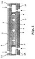
- a liquid crystal display panel A flexible substrate 2 is provided with a functional layer 3. Likewise, substrate 8 is provided with functional layer 9.
- the seals 5 can be applied on the substrate by e.g. screen printing or offset printing and are formed of e.g. an epoxy, a silicone, a urethane, or an acrylic resin. Then, a panel is assembled wherein both substrates 2 and 8, separated by spacers 4, are brought into parallel contact. The display cell is filled with liquid crystal composition 6 and finally glass sheets 1 and 7 are laminated to substrate 2 and 8 respectively.
- a panel in the method of the present invention may comprise a single or a plurality of modules.
- a panel is shown which comprises three modules. These modules can be cut from the panel at the boundary between said modules, indicated by the arrows in Fig. 1.
- the modules can be cut symmetrically (both substrates at identical positions) or asymmetrically as shown in Fig. 1, which is a typical method of cutting LCD cells from a panel.
- each module separately by laminating to the panel a plurality of adjacent glass sheets 1,11,21 and 7,17,27 of about the same size as a module in such a way that each laminated glass sheet is aligned with a module and a space is left between the laminated glass sheets, said space being aligned with the boundary between the modules.
- the substrate can by cut easily (illustrated in Fig. 1 by the dashed lines which are indicated by the arrows) at the non-laminated space using common tools such as a knife, scissors, or local melting of the substrate.
- the modules may first be cut and then laminated to a glass sheet.
- the panel can be cut by first removing the glass (e.g. by grinding a groove therein) along the boundary between the modules and then cutting the substrate as described above.
- the edges of the substrates are not covered by glass. These edges can be shielded from oxygen and water vapour by applying thereon a resin or other composition (not shown in Fig. 1) which completely covers all sides of said edges. Said resin or composition may consist of e.g. the same material as seals 5.
- the edges of the substrate can be sealed by applying two glass sheets on opposite sides of the module according to the present invention and then fusing the edges of the glass sheets together, e.g. using a high power laser. The latter method provides fully closed modules, which are completely 'wrapped up' in glass and thus effectively protected from degradation due to e.g. oxygen and water vapour.
- the present invention also covers methods wherein the glass sheet is not laminated directly to the substrate, but also methods wherein first one or more additional foils are laminated to the substrate, followed by lamination of the glass sheet(s).
- additional foils e.g. used in LCD manufacturing
- retardation film e.g. used in LCD manufacturing
- reflection or anti-reflection foil e.g. used in LCD manufacturing
- foils which improve the viewing angle e.g., light dispersion foils, polarisors, etc.
- one or more additional foil(s) may be present between the glass sheet 1 and substrate 2.
- a glass/support laminate may be laminated to the panel, either by laminating the glass side of the glass/support laminate to the panel or by laminating the support side of said laminate to the panel.
- the support of such a glass/support laminate may be e.g. one of the additional foils referred to above. More details about suitable glass/support laminates for use in the present invention can be found in WO99/21707 and WO99/21708.
- the glass used in the present invention has a thickness of not less than 10 ⁇ m and not more than 1.5 mm. To reduce the weight of the electric or electronic device, it may be preferred to use glass having a thickness less than 700 ⁇ m or even less than 500 ⁇ m.
- a flexible device can be obtained by laminating a flexible thin glass sheet, e.g. as described in EP-A-716339, to the module. For such applications, a thickness lower than 300 ⁇ m or even lower than 200 ⁇ m may be preferred. For lower brittleness a thickness of not less than 30 ⁇ m or even not less than 50 ⁇ m may be preferred.
- the glass may be e.g. sodium float glass, chemically strengthened glass or borosilicate glass. Such glass can be made by squeezing semi-molten glass between metal rollers to produce a thin web.
- US 4, 388, 368 describes the following method to produce flexible glass sheets.
- the glass thus formed is supported by clips at both ends and heated at about 350°C. Thereafter the glass sheet is stretched to from 1.05 to 10 times the area of the original sheet while blowing a hot blast of air at a temperature lower than the aforesaid heating temperature onto the glass sheet, e.g. about 700°C.
- Chemically strengthened float glass is known to have greater strength than regular float glass.
- Chemically strengthened glass is glass wherein at both surface layers the original alkali ions are at least partially replaced by alkali ions having a larger radius.
- chemically hardened sodium lime silica glass the sodium ions near the surface of the glass are at least partially substituted by potassium and in chemically hardened lithium lime silica glass, the lithium ions near the surface are at least partially substituted by sodium and/or potassium.
- Known methods for producing chemically strengthened glass are processes wherein glass is exposed to ion exchange conditions as described in e.g. JP-A 56,041,859, GB 1,208,153 and US 3,639,198. More details about chemical strengthening of glass are given in e.g. "Glass Technology", Vol. 6, No. 3, page 90-97, June 1965.
- Borosilicate glass comprises SiO 2 and B 2 O 3 .
- the detailed composition of some borosilicate glass types has been described in e.g. US-P 4,870034, 4,554,259 and 5,547,904.
- Preferred thin borosilicate glass for use in the method of the present invention is commercially available from e.g. Deutsche Spezialglass AG (Desag, Germany), a Schott Group company, as types AF45 and D263 with a thickness as low as 30 ⁇ m.
- thin borosilicate glass is available in a thickness of 30 ⁇ m, 50 ⁇ m, 70 ⁇ m, 100 ⁇ m, 145 ⁇ m, 175 ⁇ m, 210 ⁇ m, 300 ⁇ m, 400 ⁇ m, 550 ⁇ m and 700 ⁇ m.
- the flexible substrate used in the method of the present invention has preferably a thickness of less than 500 ⁇ m, more preferably less than 250 ⁇ m and most preferably less than 100 ⁇ m. It may be a metal foil, paper, or a plastic formed of one or more material(s) selected from the group consisting of polyether resin, cellulose resins such as cellulose diacetate, cellulose triacetate and butyl acetate, polyethersulfone (PES) resin, acrylic resin, poly(ethylene terephthalate) (PET) resin, phenoxy resin, phenoxy-urethane resin, urethan resin, polyether-ketone resin, polyether-ether-ketone resin, polyimide-amide resin, polycarbonate (PC) resin, polysulfone resin, polyethylene resin, or polypropylene resin.
- polyether resin cellulose resins such as cellulose diacetate, cellulose triacetate and butyl acetate
- PES polyethersulfone
- PET poly(ethylene terephthalate)
- copolymers can be used, e.g. a copolymer of acrylonitrile, styrene and butadiene or cyclo-olephine copolymers (COCs) such as copolymers comprising (poly) dicyclopentadieen (PDCP).
- COCs cyclo-olephine copolymers
- PET, PC, PES and PDCP are highly preferred.
- PES and PDCP are especially preferred for applying functional layers by high temperature processes.
- the substrate may consist of multilayers formed of some materials of the above mentioned resins.
- the substrate itself may also be or comprise a polarising film.
- Both substrates can be the same or different.
- one substrate may be a plastic film and the other a glass plate so as to obtain a hybrid device.
- One of the substrates of the module may be coated with a reflecting layer or laminated to a reflective foil, e.g. to make a reflective display.
- the glass sheet or the glass/support laminate which is laminated to the panel according to the present invention may be provided with an additional barrier layer to reduce permeability of gases such as oxygen or water vapour in case the glass sheet fractures when the device is dropped.
- Organic barrier layers may comprise e.g. poly(vinyl alcohol), polyacrylonitrile, poly(vinyl butyral), which may be mixed with an epoxy resin, or the Organically Modified Ceramic layers and the poly(hydroxy amide ethers) referred to in the background description.
- Inorganic barrier layers are typically thin films of sputtered oxides, e.g. SiO X or Ta 2 0 5 .
- the thickness of such inorganic barrier layers is preferably lower than 2 ⁇ m, and preferably about 1 ⁇ m so as to obtain some flexibility. It may be advantageous to combine inorganic and organic barrier layers, e.g. a SiO x layer overcoated with an Organically Modified Ceramic layer, since the uneven surface of an anorganic layer which is typically applied by vapour deposition or sputtering can be leveled off by overcoating with the organic layer.
- both layers may be laminated without the use of an adhesive layer by so-called vacuum lamination.
- both these materials are preferably characterised by a low surface roughness, e.g. the substrate preferably does not contain a so-called spacing agent, which is often introduced in plastic foils or in coatings on foils to prevent sticking.
- double-sided adhesive tape or an adhesive layer obtained by applying e.g. a hotmelt, a pressure- or thermo-sensitive adhesive, or a UV or electron-beam curable adhesive.
- a slightly moistened gelatine layer can also be used as an adhesive layer. More information about suitable adhesive layers is described in WO99/21707 and WO99/21708.
- the adhesive layer may be applied either to the glass sheet, to the module, or to both and may be protected by a stripping layer, which is removed just before lamination.
- Polyethylene is a highly preferred adhesive, which can be applied as a foil between the glass and the substrate.
- the functional layer can be applied on the substrate by sputtering, by physical vapour deposition, by chemical vapour deposition, as well as by coating from a liquid coating solution such as spin coating, dip coating, rod coating, blade coating, air knife coating, gravure coating, reverse roll coating, extrusion coating, slide coating and curtain coating.
- a liquid coating solution such as spin coating, dip coating, rod coating, blade coating, air knife coating, gravure coating, reverse roll coating, extrusion coating, slide coating and curtain coating.
- a plurality of layers may be coated simultaneously, e.g. by coating techniques such as slide coating or curtain coating.
- the substrate may be provided with a functional layer as a sheet or as a web. The latter is especially preferred for industrial roll-to-roll manufacturing of devices such as FPDs which may significantly reduce the cost of the process compared to the batch methods that are being used at present.
- a highly preferred FPD is an LCD.
- a typical LCD cell comprises a module of two parallel substrates which each carry on their inner surface an electroconductive layer and a liquid crystal orientation layer, also called alignment layer.
- one of the substrates is also provided with a colour filter.
- These electroconductive layers, alignment layers and colour filters shall be regarded as a functional layer which may be applied according to the method of the present invention.
- a liquid crystal orientation layer typically consists of a polyimide film which is mechanically rubbed so that the director of the liquid crystal molecules aligns itself with the rubbing direction. More information can be found in e.g. "Surface alignment of liquid crystals by rubbed polymer layers", by A. Mosley and B.M. Nicholas, published in Displays. pp.17-21, January 1987.
- Coatings consisting of tin oxide, indium oxide or tin-doped indium oxide (ITO) are widely used as electroconductive layers in FPDs because these materials possess high transparency in the visible spectrum combined with a fairly low electrical resistivity.
- ITO can be coated by e.g. RF-sputtering from an ITO target, described by J.L. Vossen in Physics of thin films, pp.1-71, Academic Press, New York (Plenum Press, 1977) or reactive DC magnetron sputtering from an indium-tin target, described in Thin Solid Films, Vol.83, pp.259-260 (1981) and Vol.72, pp.469-474 (1980), followed by thermal treatment.
- DE-A-41 32 614 discloses the production of film-forming, electroconductive polymers by anodic oxidation of pyrroles, thiophenes, furans or aromatic amines (or their derivatives) is effected with a sulphone compound present in the electrolyte solution.
- the preparation of electroconductive polythiophenes and polypyrroles is described in US 5 254 648 and in US 5 236 627 respectively.
- EP-A-440 957 a method for preparing polythiophene in an aqueous environment and applying polythiophene from an aqueous solution has been described.
- a functional layer, applied onto the substrate according to the method of the present invention may also be a non-contiguous functional layer, e.g. electroconductive patterns defining electric or electronic components such as the rows and columns used for multiplex-addressing in passive-matrix LCDs or the thin-film-transistors (TFTs) and pixel electrodes used in active-matrix LCDs.
- electroconductive patterns defining electric or electronic components such as the rows and columns used for multiplex-addressing in passive-matrix LCDs or the thin-film-transistors (TFTs) and pixel electrodes used in active-matrix LCDs.
- TFTs thin-film-transistors
- pixel electrodes used in active-matrix LCDs.
- photolithographic as well as printing techniques can be used.
- the non-continuous layer can also be formed on the substrate by other techniques, e.g. lamination followed by delamination, ink jet, toner jet, electrophotography, or thermosublimation.
- the colour filters which similarly to the above electroconductive patterns and layers are not only used in LCDs but also in other FPD types, are another example of a non-contiguous functional layer that may be applied in the method of the present invention.
- the colour filter can be a gelatine-based filter, a vacuum deposited filter, a printed filter, an interference filter, an electrolytically deposited filter, etc.
- Some suitable examples can be found in e.g. "High quality organic pigment colour filter for colour LCD” by T. Ueno, T. Motomura, S. Naemura, K. Noguchi and C. Tani in Japan Display, 1986, pp. 320-322; "An active matrix colour LCD with high transmittance using an optical interference filter" by T. Unate, T.
- the method of the present invention can be used during the manufacturing of passive-matrix LCDs as well as active-matrix LCDs such as thin-film-transistor (TFT) displays.
- TFT thin-film-transistor
- Other particular examples are twisted nematic (TN), supertwisted nematic (STN), double supertwisted nematic (DSTN), retardation film supertwisted nematic (RFSTN), ferroelectric (FLC), guest-host (GH), polymer-dispersed (PF), polymer network (PN) liquid crystal displays, and so on.
- Emissive FPD types which may benefit from the present invention are e.g. plasma displays (PDs), field emission displays (FEDs) and so-called organic light-emitting displays (OLEDs).
- PDs plasma displays
- FEDs field emission displays
- OLEDs organic light-emitting displays
- the electroconducting layers or patterns on at least one of the substrates may be replaced by a non-transparent material, e.g. silver or nickel.
- a typical PD comprises two substrates which enclose a gas-filled volume, the gas being typically one of the noble gases or a mixture thereof.
- a plasma discharge is generated which emits UV light.
- the discharges are confined to separate cells (pixels) formed by walls of insulating material between the glass substrates.
- the UV light may excite phosphors which are present on the cell walls so as to obtain colour images.
- colour filters are also used in PDs.
- the electroconductive layers or patterns may be shielded from the plasma by applying a dielectric protecting layer, which comprises e.g. lead oxide or magnesium oxide.
- said insulating walls, phosphors, colour filters and dielectric protecting layers shall be regarded as a (non-contiguous) functional layer which may be applied in the method of the present invention.
- FEDs also comprise two substrates which are provided with functional layers.
- one of the substrates of a FED is provided with a large number of microtips, consisting of e.g. molybdenum, which each act as a microscopic electron gun.
- microtips consisting of e.g. molybdenum, which each act as a microscopic electron gun.
- these microtips When charged up to a high voltage from 200 to 800 V, these microtips emit an electron beam towards a phosphor layer on the opposite substrate which typically carries an ITO layer as a counter electrode.
- the electroconductive layers and patterns, microtips and phosphor layers in FEDs shall also be regarded as functional layers which may be applied in the method of the present invention.
- OLEDs are electroluminescent devices wherein electrons and holes are injected from a cathode and anode respectively into an electroluminescent material, e.g. an electroluminescent polymer such as poly(p-phenylenevinylene) (PPV) and its derivatives, fluorene derivatives or distyrylbenzene compounds, and then recombine to an exciton which relaxes to the ground state by radiative decay.
- PV poly(p-phenylenevinylene)
- a preferred device made according to the present invention is fully composed of organic layers (excluding the glass sheets) as such layers are resistant to bending, distinguished from brittle inorganic layers such as ITO.
- Such devices may comprise e.g. all-organic thin-film-transistors as described in Adv. Mater. vol. 2, no. 12, p.592 (1990).
- electrolytic capacitors In addition to the FPDs above, other suitable examples of devices which may be obtained by the present invention are electrolytic capacitors, circuit boards, electrochromic displays, an electronic book such as the one described in WO 97/04398 or a photovoltaic device such as an organic solar cell which comprises a similar structure as the OLED described above, with the proviso that the electroluminescent layer is replaced by a composition wherein photo-induced electron transfer occurs between an electron-donor and an acceptor.
- a similar device as shown in Fig.1 was prepared.
- a flexible plastic film consisting of a phenoxy-urethan polymer according to the following formula was used as a substrate : wherein C 6 H 4 is a phenyl group.
- An ITO layer having a thickness of 500 ⁇ was applied on one side of the plastic substrate by low temperature sputtering and then patterned into electrodes by photolithography.
- a polyimide resin was coated on the electrode surface at a thickness of 500 ⁇ , dried at 150 °C for 1 hour and then rubbed with gauze in one direction so as to obtain a liquid crystal orientation layer. The material thus obtained formed a first substrate.
- a similar material was prepared as second substrate.
- a flexible epoxy adhesive was screenprinted onto the surface of the first substrate in a sealing pattern.
- a silver-based conductive adhesive was applied to both substrates to form electric contacts. Fine particles of glass fibre having a diameter of 10 ⁇ m were scattered on the first substrate and then both substrates were assembled to form a panel and cured by heating at 100 °C during 1 hour. Said panel consisted of a single LCD cell.
- a liquid crystal composition was injected into the space between both substrates and the seals by vacuum injection. The injection inlet was sealed with an epoxy resin to obtain a liquid crystal display cell.
- a polyethylene adhesive layer was then spin-coated on both outer surfaces of the panel.
- two borosilicate glass sheets of type AF45 (Schott Glass, Germany) having a thickness of 70 ⁇ m were laminated to both sides of the panel.
- a low-weight, flexible display was obtained which is well protected from oxygen, water vapour, heat and mechanical impact.
Abstract
Description
- a reflecting cathode, e.g. a low-work function metal layer such as evaporated Ca.
- an electroluminescent layer, e.g. PPV; other suitable electroluminescent compounds are described in e.g. "Organische Leuchtdioden", Chemie in unserer Zeit, 31. Jahrg. 1997, No.2, p. 76-86 .
- an hole-injection layer, e.g. an organic electroconductive layer.
- an transparent anode, e.g. an ITO layer

Claims (10)
- A method of making a module for use in an electric or electronic device such as a flat panel display, a light emitting diode or a photovoltaic cell, said method comprising the steps of(i) providing a flexible substrate with a functional layer;(ii) bringing said flexible substrate into parallel contact with another substrate so as to obtain a module wherein the functional layer is present between both substrates;(iii) laminating a glass sheet having a thickness in the range from 10 µm to 0.7 mm to at least one side of the module.
- A method of making a module for use in an electric or electronic device such as a flat panel display, a light emitting diode or a photovoltaic cell, said method comprising the steps of(i) providing a flexible substrate with a functional layer;(ii) bringing said flexible substrate into parallel contact with another substrate so as to obtain a panel wherein the functional layer is present between both substrates, said panel comprising a plurality of adjacent modules which are mutually separated by a boundary between said modules;(iii) laminating a plurality of glass sheets having a thickness in the range from 10 µm to 1.5 mm to at least one side of the panel, wherein the laminated glass sheets are aligned with the modules and are mutually spaced at the boundary between the modules.
- A method of making a module for use in an electric or electronic device such as a flat panel display, a light emitting diode or a photovoltaic cell, said method comprising the steps of(i) providing a flexible substrate with a functional layer;(ii) bringing said flexible substrate into parallel contact with another substrate so as to obtain a panel wherein the functional layer is present between both substrates, said panel comprising a plurality of adjacent modules which are mutually separated by a boundary between said modules;(iii) cutting the modules at the boundary between said modules;(iv) laminating a plurality of glass sheets having a thickness in the range from 10 µm to 1.5 mm to at least one side of a module.
- A method according to claim 2 or 3 wherein the thickness of the glass is in the range from 10 to 700 µm.
- A method according to any of claim 1 to 3 wherein the thickness of the glass is in the range from 30 to 500 µm.
- A method according to any of claim 1 to 3 wherein the thickness of the glass is in the range from 50 to 300 µm.
- A method according to any of the previous claims wherein the glass is flexible.
- A method according to any of the previous claims wherein the glass is borosilicate or chemically hardened glass.
- A method according to any of the previous claims wherein step (i) is carried out by a printing process or a web coating process.
- A method according to any of the previous claims wherein the glass is replaced by a glass/support laminate.
Priority Applications (1)
| Application Number | Priority Date | Filing Date | Title |
|---|---|---|---|
| EP00200799A EP1038663B1 (en) | 1999-03-26 | 2000-03-06 | Method of making an electronic module comprising a glass laminate |
Applications Claiming Priority (3)
| Application Number | Priority Date | Filing Date | Title |
|---|---|---|---|
| EP99200956 | 1999-03-26 | ||
| EP99200956 | 1999-03-26 | ||
| EP00200799A EP1038663B1 (en) | 1999-03-26 | 2000-03-06 | Method of making an electronic module comprising a glass laminate |
Publications (3)
| Publication Number | Publication Date |
|---|---|
| EP1038663A2 true EP1038663A2 (en) | 2000-09-27 |
| EP1038663A3 EP1038663A3 (en) | 2002-03-27 |
| EP1038663B1 EP1038663B1 (en) | 2012-12-19 |
Family
ID=26071958
Family Applications (1)
| Application Number | Title | Priority Date | Filing Date |
|---|---|---|---|
| EP00200799A Expired - Lifetime EP1038663B1 (en) | 1999-03-26 | 2000-03-06 | Method of making an electronic module comprising a glass laminate |
Country Status (1)
| Country | Link |
|---|---|
| EP (1) | EP1038663B1 (en) |
Cited By (27)
| Publication number | Priority date | Publication date | Assignee | Title |
|---|---|---|---|---|
| WO2003055676A1 (en) * | 2002-01-04 | 2003-07-10 | Basf Aktiengesellschaft | Flexible glass/polymer composite |
| EP1447706A2 (en) | 2003-02-13 | 2004-08-18 | Eastman Kodak Company | Polymer dispersed cholesteric liquid crystal display device and method of manufacturing thereof |
| WO2005110741A1 (en) * | 2004-05-19 | 2005-11-24 | Dsm Ip Assets B.V. | Process for composite layered material for electronic optical devices |
| US7033850B2 (en) | 2004-06-30 | 2006-04-25 | Eastman Kodak Company | Roll-to-sheet manufacture of OLED materials |
| DE102007025687B3 (en) * | 2007-06-01 | 2009-01-08 | Schott Ag | Use of a borosilicate glass sheet in a flat display device and flat display device with this glass sheet |
| DE102008041278A1 (en) | 2008-08-15 | 2010-02-18 | Evonik Degussa Gmbh | Use of polyolefins as adhesion promoters for the production of laminates |
| WO2012103190A1 (en) * | 2011-01-27 | 2012-08-02 | Corning Incorporated | Laminated pv module package |
| CN101626987B (en) * | 2007-01-30 | 2012-09-05 | 康宁股份有限公司 | Ultra thin glass drawing and blowing |
| WO2012174179A1 (en) * | 2011-06-15 | 2012-12-20 | Dow Global Technologies Llc | Flexible photovoltaic articles |
| WO2014028128A1 (en) * | 2012-08-14 | 2014-02-20 | Apple Inc. | Display with bent inactive edge regions |
| WO2015130494A3 (en) * | 2014-02-28 | 2015-10-15 | Apple Inc. | Exposed glass article with enhanced stiffness for portable electronic device housing |
| US9439305B2 (en) | 2010-09-17 | 2016-09-06 | Apple Inc. | Glass enclosure |
| US9459661B2 (en) | 2013-06-19 | 2016-10-04 | Apple Inc. | Camouflaged openings in electronic device housings |
| US9516149B2 (en) | 2011-09-29 | 2016-12-06 | Apple Inc. | Multi-layer transparent structures for electronic device housings |
| US9513664B2 (en) | 2011-05-04 | 2016-12-06 | Apple Inc. | Housing for portable electronic device with reduced border region |
| US9615448B2 (en) | 2008-06-27 | 2017-04-04 | Apple Inc. | Method for fabricating thin sheets of glass |
| US9684339B2 (en) | 2015-02-03 | 2017-06-20 | Microsoft Technology Licensing, Llc | Bendable display assembly |
| US9725359B2 (en) | 2011-03-16 | 2017-08-08 | Apple Inc. | Electronic device having selectively strengthened glass |
| US9756739B2 (en) | 2012-01-25 | 2017-09-05 | Apple Inc. | Glass device housing |
| US9778685B2 (en) | 2011-05-04 | 2017-10-03 | Apple Inc. | Housing for portable electronic device with reduced border region |
| US9946302B2 (en) | 2012-09-19 | 2018-04-17 | Apple Inc. | Exposed glass article with inner recessed area for portable electronic device housing |
| US9944554B2 (en) | 2011-09-15 | 2018-04-17 | Apple Inc. | Perforated mother sheet for partial edge chemical strengthening and method therefor |
| US10133156B2 (en) | 2012-01-10 | 2018-11-20 | Apple Inc. | Fused opaque and clear glass for camera or display window |
| US10144669B2 (en) | 2011-11-21 | 2018-12-04 | Apple Inc. | Self-optimizing chemical strengthening bath for glass |
| US10185113B2 (en) | 2009-03-02 | 2019-01-22 | Apple Inc. | Techniques for strengthening glass covers for portable electronic devices |
| US10189743B2 (en) | 2010-08-18 | 2019-01-29 | Apple Inc. | Enhanced strengthening of glass |
| US10781135B2 (en) | 2011-03-16 | 2020-09-22 | Apple Inc. | Strengthening variable thickness glass |
Families Citing this family (1)
| Publication number | Priority date | Publication date | Assignee | Title |
|---|---|---|---|---|
| US10029941B2 (en) | 2014-03-31 | 2018-07-24 | Corning Incorporated | Machining methods of forming laminated glass structures |
Citations (1)
| Publication number | Priority date | Publication date | Assignee | Title |
|---|---|---|---|---|
| DE4038498A1 (en) | 1990-12-03 | 1992-06-04 | Trebe Elektronik Inh Joannis T | Plastics foil with controllable transparency - comprises liq. crystal layer between polyvinyl chloride foil layers, for blind slat, window coating and composite glass interlayer |
Family Cites Families (4)
| Publication number | Priority date | Publication date | Assignee | Title |
|---|---|---|---|---|
| US3944461A (en) * | 1974-11-18 | 1976-03-16 | Globe Glass & Trim Company | Machine for laminating glass |
| US5091258A (en) * | 1990-08-20 | 1992-02-25 | Monsanto Company | Laminate for a safety glazing |
| EP0840653B1 (en) * | 1995-07-24 | 2004-06-30 | Southwall Technologies, Inc. | Improved laminate structure and process for its production |
| DE69806263T2 (en) * | 1997-10-24 | 2009-09-24 | Agfa-Gevaert | CONNECTED WASHER WITH A THIN BOROSILICATE GLASS STRIP AS A FORMING LAYER |
-
2000
- 2000-03-06 EP EP00200799A patent/EP1038663B1/en not_active Expired - Lifetime
Patent Citations (1)
| Publication number | Priority date | Publication date | Assignee | Title |
|---|---|---|---|---|
| DE4038498A1 (en) | 1990-12-03 | 1992-06-04 | Trebe Elektronik Inh Joannis T | Plastics foil with controllable transparency - comprises liq. crystal layer between polyvinyl chloride foil layers, for blind slat, window coating and composite glass interlayer |
Cited By (55)
| Publication number | Priority date | Publication date | Assignee | Title |
|---|---|---|---|---|
| WO2003055676A1 (en) * | 2002-01-04 | 2003-07-10 | Basf Aktiengesellschaft | Flexible glass/polymer composite |
| EP1447706A2 (en) | 2003-02-13 | 2004-08-18 | Eastman Kodak Company | Polymer dispersed cholesteric liquid crystal display device and method of manufacturing thereof |
| EP1447706B1 (en) * | 2003-02-13 | 2009-03-11 | Industrial Technology Research Institute | Polymer dispersed cholesteric liquid crystal display device and method of manufacturing thereof |
| WO2005110741A1 (en) * | 2004-05-19 | 2005-11-24 | Dsm Ip Assets B.V. | Process for composite layered material for electronic optical devices |
| US7033850B2 (en) | 2004-06-30 | 2006-04-25 | Eastman Kodak Company | Roll-to-sheet manufacture of OLED materials |
| CN101626987B (en) * | 2007-01-30 | 2012-09-05 | 康宁股份有限公司 | Ultra thin glass drawing and blowing |
| DE102007025687B3 (en) * | 2007-06-01 | 2009-01-08 | Schott Ag | Use of a borosilicate glass sheet in a flat display device and flat display device with this glass sheet |
| US9615448B2 (en) | 2008-06-27 | 2017-04-04 | Apple Inc. | Method for fabricating thin sheets of glass |
| US9550344B2 (en) | 2008-08-15 | 2017-01-24 | Evonik Degussa Gmbh | Use of silane-modified polyolefins as adhesion promoters for the production flat laminates |
| WO2010018034A1 (en) * | 2008-08-15 | 2010-02-18 | Evonik Degussa Gmbh | Use of silane-modified plyolefins as adhesion promoters for the production of flat laminates |
| DE102008041278A1 (en) | 2008-08-15 | 2010-02-18 | Evonik Degussa Gmbh | Use of polyolefins as adhesion promoters for the production of laminates |
| US10185113B2 (en) | 2009-03-02 | 2019-01-22 | Apple Inc. | Techniques for strengthening glass covers for portable electronic devices |
| US10189743B2 (en) | 2010-08-18 | 2019-01-29 | Apple Inc. | Enhanced strengthening of glass |
| US9439305B2 (en) | 2010-09-17 | 2016-09-06 | Apple Inc. | Glass enclosure |
| US10021798B2 (en) | 2010-09-17 | 2018-07-10 | Apple Inc. | Glass enclosure |
| US11785729B2 (en) | 2010-09-17 | 2023-10-10 | Apple Inc. | Glass enclosure |
| US10398043B2 (en) | 2010-09-17 | 2019-08-27 | Apple Inc. | Glass enclosure |
| US10765020B2 (en) | 2010-09-17 | 2020-09-01 | Apple Inc. | Glass enclosure |
| WO2012103190A1 (en) * | 2011-01-27 | 2012-08-02 | Corning Incorporated | Laminated pv module package |
| US11518708B2 (en) | 2011-03-16 | 2022-12-06 | Apple Inc. | Electronic device having selectively strengthened glass |
| US10676393B2 (en) | 2011-03-16 | 2020-06-09 | Apple Inc. | Electronic device having selectively strengthened glass |
| US9725359B2 (en) | 2011-03-16 | 2017-08-08 | Apple Inc. | Electronic device having selectively strengthened glass |
| US10781135B2 (en) | 2011-03-16 | 2020-09-22 | Apple Inc. | Strengthening variable thickness glass |
| US9778685B2 (en) | 2011-05-04 | 2017-10-03 | Apple Inc. | Housing for portable electronic device with reduced border region |
| US10656674B2 (en) | 2011-05-04 | 2020-05-19 | Apple Inc. | Housing for portable electronic device with reduced border region |
| US10983557B2 (en) | 2011-05-04 | 2021-04-20 | Apple Inc. | Housing for portable electronic device with reduced border region |
| US9513664B2 (en) | 2011-05-04 | 2016-12-06 | Apple Inc. | Housing for portable electronic device with reduced border region |
| US10401904B2 (en) | 2011-05-04 | 2019-09-03 | Apple Inc. | Housing for portable electronic device with reduced border region |
| US10761563B2 (en) | 2011-05-04 | 2020-09-01 | Apple Inc. | Housing for portable electronic device with reduced border region |
| US11681326B2 (en) | 2011-05-04 | 2023-06-20 | Apple Inc. | Housing for portable electronic device with reduced border region |
| WO2012174179A1 (en) * | 2011-06-15 | 2012-12-20 | Dow Global Technologies Llc | Flexible photovoltaic articles |
| US9944554B2 (en) | 2011-09-15 | 2018-04-17 | Apple Inc. | Perforated mother sheet for partial edge chemical strengthening and method therefor |
| US11368566B2 (en) | 2011-09-29 | 2022-06-21 | Apple Inc. | Multi-layer transparent structures for electronic device housings |
| US10320959B2 (en) | 2011-09-29 | 2019-06-11 | Apple Inc. | Multi-layer transparent structures for electronic device housings |
| US9516149B2 (en) | 2011-09-29 | 2016-12-06 | Apple Inc. | Multi-layer transparent structures for electronic device housings |
| US10574800B2 (en) | 2011-09-29 | 2020-02-25 | Apple Inc. | Multi-layer transparent structures for electronic device housings |
| US10144669B2 (en) | 2011-11-21 | 2018-12-04 | Apple Inc. | Self-optimizing chemical strengthening bath for glass |
| US10551722B2 (en) | 2012-01-10 | 2020-02-04 | Apple Inc. | Fused opaque and clear glass for camera or display window |
| US10133156B2 (en) | 2012-01-10 | 2018-11-20 | Apple Inc. | Fused opaque and clear glass for camera or display window |
| US9756739B2 (en) | 2012-01-25 | 2017-09-05 | Apple Inc. | Glass device housing |
| US11260489B2 (en) | 2012-01-25 | 2022-03-01 | Apple Inc. | Glass device housings |
| US11612975B2 (en) | 2012-01-25 | 2023-03-28 | Apple Inc. | Glass device housings |
| US10278294B2 (en) | 2012-01-25 | 2019-04-30 | Apple Inc. | Glass device housings |
| US10842031B2 (en) | 2012-01-25 | 2020-11-17 | Apple Inc. | Glass device housings |
| US10512176B2 (en) | 2012-01-25 | 2019-12-17 | Apple Inc. | Glass device housings |
| US9110320B2 (en) | 2012-08-14 | 2015-08-18 | Apple Inc. | Display with bent inactive edge regions |
| WO2014028128A1 (en) * | 2012-08-14 | 2014-02-20 | Apple Inc. | Display with bent inactive edge regions |
| US9946302B2 (en) | 2012-09-19 | 2018-04-17 | Apple Inc. | Exposed glass article with inner recessed area for portable electronic device housing |
| US9459661B2 (en) | 2013-06-19 | 2016-10-04 | Apple Inc. | Camouflaged openings in electronic device housings |
| US10496135B2 (en) | 2014-02-28 | 2019-12-03 | Apple Inc. | Exposed glass article with enhanced stiffness for portable electronic device housing |
| US9886062B2 (en) | 2014-02-28 | 2018-02-06 | Apple Inc. | Exposed glass article with enhanced stiffness for portable electronic device housing |
| WO2015130494A3 (en) * | 2014-02-28 | 2015-10-15 | Apple Inc. | Exposed glass article with enhanced stiffness for portable electronic device housing |
| US10579101B2 (en) | 2014-02-28 | 2020-03-03 | Apple Inc. | Exposed glass article with enhanced stiffness for portable electronic device housing |
| US10509440B2 (en) | 2015-02-03 | 2019-12-17 | Microsoft Technology Licensing, Llc | Bendable display assembly |
| US9684339B2 (en) | 2015-02-03 | 2017-06-20 | Microsoft Technology Licensing, Llc | Bendable display assembly |
Also Published As
| Publication number | Publication date |
|---|---|
| EP1038663B1 (en) | 2012-12-19 |
| EP1038663A3 (en) | 2002-03-27 |
Similar Documents
| Publication | Publication Date | Title |
|---|---|---|
| US6355125B1 (en) | Method for making an electric or electronic module comprising a glass laminate | |
| EP1038663B1 (en) | Method of making an electronic module comprising a glass laminate | |
| EP1098761B1 (en) | Segmented glass laminate | |
| EP1024953B1 (en) | Use of glass laminate as a substrate in semiconductor devices | |
| EP1037862B1 (en) | Flexible substrate | |
| US7850814B2 (en) | Polymeric conductor donor and transfer method | |
| US7410825B2 (en) | Metal and electronically conductive polymer transfer | |
| US6689626B2 (en) | Flexible substrate | |
| KR19980079255A (en) | Substrate to which a transparent conductive film is attached and a display element using the same | |
| CN101351738A (en) | Flexible display apparatus and method for producing the same | |
| JP4864186B2 (en) | Method for manufacturing electrically conductive substrate | |
| KR101127230B1 (en) | flexible display substrate | |
| CN111863902B (en) | Display panel, display panel preparation method and display device | |
| JP4819211B2 (en) | Method for manufacturing electrical or electronic modules containing glass laminates | |
| KR20110052759A (en) | A method for manufacturing a flexible display | |
| KR102018336B1 (en) | conductive stacked film and manufacturing method thereof | |
| JPH0389412A (en) | Transparent conductive film |
Legal Events
| Date | Code | Title | Description |
|---|---|---|---|
| PUAI | Public reference made under article 153(3) epc to a published international application that has entered the european phase |
Free format text: ORIGINAL CODE: 0009012 |
|
| AK | Designated contracting states |
Kind code of ref document: A2 Designated state(s): AT BE CH CY DE DK ES FI FR GB GR IE IT LI LU MC NL PT SE Kind code of ref document: A2 Designated state(s): DE FR GB |
|
| AX | Request for extension of the european patent |
Free format text: AL;LT;LV;MK;RO;SI |
|
| PUAL | Search report despatched |
Free format text: ORIGINAL CODE: 0009013 |
|
| RAP1 | Party data changed (applicant data changed or rights of an application transferred) |
Owner name: AGFA-GEVAERT |
|
| AK | Designated contracting states |
Kind code of ref document: A3 Designated state(s): AT BE CH CY DE DK ES FI FR GB GR IE IT LI LU MC NL PT SE |
|
| AX | Request for extension of the european patent |
Free format text: AL;LT;LV;MK;RO;SI |
|
| RIC1 | Information provided on ipc code assigned before grant |
Free format text: 7G 02F 1/1333 A, 7B 32B 17/10 B |
|
| 17P | Request for examination filed |
Effective date: 20020927 |
|
| AKX | Designation fees paid |
Free format text: DE FR GB |
|
| 17Q | First examination report despatched |
Effective date: 20040908 |
|
| RAP1 | Party data changed (applicant data changed or rights of an application transferred) |
Owner name: CHI MEI OPTOELECTRONICS CORPORATION |
|
| RAP3 | Party data changed (applicant data changed or rights of an application transferred) |
Owner name: CHI MEI OPTOELECTRONICS CORPORATION |
|
| 17Q | First examination report despatched |
Effective date: 20040908 |
|
| GRAP | Despatch of communication of intention to grant a patent |
Free format text: ORIGINAL CODE: EPIDOSNIGR1 |
|
| GRAS | Grant fee paid |
Free format text: ORIGINAL CODE: EPIDOSNIGR3 |
|
| GRAA | (expected) grant |
Free format text: ORIGINAL CODE: 0009210 |
|
| RAP1 | Party data changed (applicant data changed or rights of an application transferred) |
Owner name: CHIMEI INNOLUX CORPORATION |
|
| AK | Designated contracting states |
Kind code of ref document: B1 Designated state(s): DE FR GB |
|
| REG | Reference to a national code |
Ref country code: GB Ref legal event code: FG4D |
|
| REG | Reference to a national code |
Ref country code: DE Ref legal event code: R096 Ref document number: 60047706 Country of ref document: DE Effective date: 20130214 |
|
| PLBE | No opposition filed within time limit |
Free format text: ORIGINAL CODE: 0009261 |
|
| STAA | Information on the status of an ep patent application or granted ep patent |
Free format text: STATUS: NO OPPOSITION FILED WITHIN TIME LIMIT |
|
| 26N | No opposition filed |
Effective date: 20130920 |
|
| REG | Reference to a national code |
Ref country code: DE Ref legal event code: R097 Ref document number: 60047706 Country of ref document: DE Effective date: 20130920 |
|
| REG | Reference to a national code |
Ref country code: FR Ref legal event code: PLFP Year of fee payment: 17 |
|
| PGFP | Annual fee paid to national office [announced via postgrant information from national office to epo] |
Ref country code: GB Payment date: 20160329 Year of fee payment: 17 Ref country code: FR Payment date: 20160328 Year of fee payment: 17 |
|
| PGFP | Annual fee paid to national office [announced via postgrant information from national office to epo] |
Ref country code: DE Payment date: 20160331 Year of fee payment: 17 |
|
| REG | Reference to a national code |
Ref country code: DE Ref legal event code: R119 Ref document number: 60047706 Country of ref document: DE |
|
| GBPC | Gb: european patent ceased through non-payment of renewal fee |
Effective date: 20170306 |
|
| REG | Reference to a national code |
Ref country code: FR Ref legal event code: ST Effective date: 20171130 |
|
| PG25 | Lapsed in a contracting state [announced via postgrant information from national office to epo] |
Ref country code: FR Free format text: LAPSE BECAUSE OF NON-PAYMENT OF DUE FEES Effective date: 20170331 Ref country code: DE Free format text: LAPSE BECAUSE OF NON-PAYMENT OF DUE FEES Effective date: 20171003 |
|
| PG25 | Lapsed in a contracting state [announced via postgrant information from national office to epo] |
Ref country code: GB Free format text: LAPSE BECAUSE OF NON-PAYMENT OF DUE FEES Effective date: 20170306 |