EP1038307B1 - Surface modification of semiconductors using electromagnetic radiation - Google Patents
Surface modification of semiconductors using electromagnetic radiation Download PDFInfo
- Publication number
- EP1038307B1 EP1038307B1 EP98960398.0A EP98960398A EP1038307B1 EP 1038307 B1 EP1038307 B1 EP 1038307B1 EP 98960398 A EP98960398 A EP 98960398A EP 1038307 B1 EP1038307 B1 EP 1038307B1
- Authority
- EP
- European Patent Office
- Prior art keywords
- deposition
- film
- semiconductor wafer
- radiation
- deposited
- Prior art date
- Legal status (The legal status is an assumption and is not a legal conclusion. Google has not performed a legal analysis and makes no representation as to the accuracy of the status listed.)
- Expired - Lifetime
Links
Images
Classifications
-
- H—ELECTRICITY
- H01—ELECTRIC ELEMENTS
- H01L—SEMICONDUCTOR DEVICES NOT COVERED BY CLASS H10
- H01L21/00—Processes or apparatus adapted for the manufacture or treatment of semiconductor or solid state devices or of parts thereof
-
- H—ELECTRICITY
- H01—ELECTRIC ELEMENTS
- H01L—SEMICONDUCTOR DEVICES NOT COVERED BY CLASS H10
- H01L21/00—Processes or apparatus adapted for the manufacture or treatment of semiconductor or solid state devices or of parts thereof
- H01L21/02—Manufacture or treatment of semiconductor devices or of parts thereof
- H01L21/02104—Forming layers
- H01L21/02107—Forming insulating materials on a substrate
- H01L21/02109—Forming insulating materials on a substrate characterised by the type of layer, e.g. type of material, porous/non-porous, pre-cursors, mixtures or laminates
- H01L21/02112—Forming insulating materials on a substrate characterised by the type of layer, e.g. type of material, porous/non-porous, pre-cursors, mixtures or laminates characterised by the material of the layer
- H01L21/02123—Forming insulating materials on a substrate characterised by the type of layer, e.g. type of material, porous/non-porous, pre-cursors, mixtures or laminates characterised by the material of the layer the material containing silicon
- H01L21/02164—Forming insulating materials on a substrate characterised by the type of layer, e.g. type of material, porous/non-porous, pre-cursors, mixtures or laminates characterised by the material of the layer the material containing silicon the material being a silicon oxide, e.g. SiO2
-
- C—CHEMISTRY; METALLURGY
- C23—COATING METALLIC MATERIAL; COATING MATERIAL WITH METALLIC MATERIAL; CHEMICAL SURFACE TREATMENT; DIFFUSION TREATMENT OF METALLIC MATERIAL; COATING BY VACUUM EVAPORATION, BY SPUTTERING, BY ION IMPLANTATION OR BY CHEMICAL VAPOUR DEPOSITION, IN GENERAL; INHIBITING CORROSION OF METALLIC MATERIAL OR INCRUSTATION IN GENERAL
- C23C—COATING METALLIC MATERIAL; COATING MATERIAL WITH METALLIC MATERIAL; SURFACE TREATMENT OF METALLIC MATERIAL BY DIFFUSION INTO THE SURFACE, BY CHEMICAL CONVERSION OR SUBSTITUTION; COATING BY VACUUM EVAPORATION, BY SPUTTERING, BY ION IMPLANTATION OR BY CHEMICAL VAPOUR DEPOSITION, IN GENERAL
- C23C16/00—Chemical coating by decomposition of gaseous compounds, without leaving reaction products of surface material in the coating, i.e. chemical vapour deposition [CVD] processes
- C23C16/02—Pretreatment of the material to be coated
- C23C16/0227—Pretreatment of the material to be coated by cleaning or etching
- C23C16/0236—Pretreatment of the material to be coated by cleaning or etching by etching with a reactive gas
-
- H—ELECTRICITY
- H01—ELECTRIC ELEMENTS
- H01L—SEMICONDUCTOR DEVICES NOT COVERED BY CLASS H10
- H01L21/00—Processes or apparatus adapted for the manufacture or treatment of semiconductor or solid state devices or of parts thereof
- H01L21/02—Manufacture or treatment of semiconductor devices or of parts thereof
- H01L21/02104—Forming layers
- H01L21/02107—Forming insulating materials on a substrate
- H01L21/02225—Forming insulating materials on a substrate characterised by the process for the formation of the insulating layer
- H01L21/0226—Forming insulating materials on a substrate characterised by the process for the formation of the insulating layer formation by a deposition process
- H01L21/02263—Forming insulating materials on a substrate characterised by the process for the formation of the insulating layer formation by a deposition process deposition from the gas or vapour phase
- H01L21/02271—Forming insulating materials on a substrate characterised by the process for the formation of the insulating layer formation by a deposition process deposition from the gas or vapour phase deposition by decomposition or reaction of gaseous or vapour phase compounds, i.e. chemical vapour deposition
-
- H—ELECTRICITY
- H01—ELECTRIC ELEMENTS
- H01L—SEMICONDUCTOR DEVICES NOT COVERED BY CLASS H10
- H01L21/00—Processes or apparatus adapted for the manufacture or treatment of semiconductor or solid state devices or of parts thereof
- H01L21/02—Manufacture or treatment of semiconductor devices or of parts thereof
- H01L21/02104—Forming layers
- H01L21/02107—Forming insulating materials on a substrate
- H01L21/02296—Forming insulating materials on a substrate characterised by the treatment performed before or after the formation of the layer
- H01L21/02299—Forming insulating materials on a substrate characterised by the treatment performed before or after the formation of the layer pre-treatment
- H01L21/0231—Forming insulating materials on a substrate characterised by the treatment performed before or after the formation of the layer pre-treatment treatment by exposure to electromagnetic radiation, e.g. UV light
-
- H—ELECTRICITY
- H01—ELECTRIC ELEMENTS
- H01L—SEMICONDUCTOR DEVICES NOT COVERED BY CLASS H10
- H01L21/00—Processes or apparatus adapted for the manufacture or treatment of semiconductor or solid state devices or of parts thereof
- H01L21/02—Manufacture or treatment of semiconductor devices or of parts thereof
- H01L21/04—Manufacture or treatment of semiconductor devices or of parts thereof the devices having at least one potential-jump barrier or surface barrier, e.g. PN junction, depletion layer or carrier concentration layer
- H01L21/18—Manufacture or treatment of semiconductor devices or of parts thereof the devices having at least one potential-jump barrier or surface barrier, e.g. PN junction, depletion layer or carrier concentration layer the devices having semiconductor bodies comprising elements of Group IV of the Periodic System or AIIIBV compounds with or without impurities, e.g. doping materials
- H01L21/30—Treatment of semiconductor bodies using processes or apparatus not provided for in groups H01L21/20 - H01L21/26
- H01L21/31—Treatment of semiconductor bodies using processes or apparatus not provided for in groups H01L21/20 - H01L21/26 to form insulating layers thereon, e.g. for masking or by using photolithographic techniques; After treatment of these layers; Selection of materials for these layers
- H01L21/314—Inorganic layers
- H01L21/316—Inorganic layers composed of oxides or glassy oxides or oxide based glass
- H01L21/31604—Deposition from a gas or vapour
- H01L21/31608—Deposition of SiO2
- H01L21/31612—Deposition of SiO2 on a silicon body
-
- H—ELECTRICITY
- H01—ELECTRIC ELEMENTS
- H01L—SEMICONDUCTOR DEVICES NOT COVERED BY CLASS H10
- H01L21/00—Processes or apparatus adapted for the manufacture or treatment of semiconductor or solid state devices or of parts thereof
- H01L21/70—Manufacture or treatment of devices consisting of a plurality of solid state components formed in or on a common substrate or of parts thereof; Manufacture of integrated circuit devices or of parts thereof
- H01L21/71—Manufacture of specific parts of devices defined in group H01L21/70
- H01L21/76—Making of isolation regions between components
- H01L21/762—Dielectric regions, e.g. EPIC dielectric isolation, LOCOS; Trench refilling techniques, SOI technology, use of channel stoppers
- H01L21/76224—Dielectric regions, e.g. EPIC dielectric isolation, LOCOS; Trench refilling techniques, SOI technology, use of channel stoppers using trench refilling with dielectric materials
- H01L21/76232—Dielectric regions, e.g. EPIC dielectric isolation, LOCOS; Trench refilling techniques, SOI technology, use of channel stoppers using trench refilling with dielectric materials of trenches having a shape other than rectangular or V-shape, e.g. rounded corners, oblique or rounded trench walls
-
- H—ELECTRICITY
- H01—ELECTRIC ELEMENTS
- H01L—SEMICONDUCTOR DEVICES NOT COVERED BY CLASS H10
- H01L21/00—Processes or apparatus adapted for the manufacture or treatment of semiconductor or solid state devices or of parts thereof
- H01L21/02—Manufacture or treatment of semiconductor devices or of parts thereof
- H01L21/04—Manufacture or treatment of semiconductor devices or of parts thereof the devices having at least one potential-jump barrier or surface barrier, e.g. PN junction, depletion layer or carrier concentration layer
- H01L21/18—Manufacture or treatment of semiconductor devices or of parts thereof the devices having at least one potential-jump barrier or surface barrier, e.g. PN junction, depletion layer or carrier concentration layer the devices having semiconductor bodies comprising elements of Group IV of the Periodic System or AIIIBV compounds with or without impurities, e.g. doping materials
- H01L21/30—Treatment of semiconductor bodies using processes or apparatus not provided for in groups H01L21/20 - H01L21/26
- H01L21/31—Treatment of semiconductor bodies using processes or apparatus not provided for in groups H01L21/20 - H01L21/26 to form insulating layers thereon, e.g. for masking or by using photolithographic techniques; After treatment of these layers; Selection of materials for these layers
- H01L21/314—Inorganic layers
- H01L21/316—Inorganic layers composed of oxides or glassy oxides or oxide based glass
- H01L21/31604—Deposition from a gas or vapour
- H01L21/31625—Deposition of boron or phosphorus doped silicon oxide, e.g. BSG, PSG, BPSG
-
- H—ELECTRICITY
- H01—ELECTRIC ELEMENTS
- H01L—SEMICONDUCTOR DEVICES NOT COVERED BY CLASS H10
- H01L21/00—Processes or apparatus adapted for the manufacture or treatment of semiconductor or solid state devices or of parts thereof
- H01L21/02—Manufacture or treatment of semiconductor devices or of parts thereof
- H01L21/04—Manufacture or treatment of semiconductor devices or of parts thereof the devices having at least one potential-jump barrier or surface barrier, e.g. PN junction, depletion layer or carrier concentration layer
- H01L21/18—Manufacture or treatment of semiconductor devices or of parts thereof the devices having at least one potential-jump barrier or surface barrier, e.g. PN junction, depletion layer or carrier concentration layer the devices having semiconductor bodies comprising elements of Group IV of the Periodic System or AIIIBV compounds with or without impurities, e.g. doping materials
- H01L21/30—Treatment of semiconductor bodies using processes or apparatus not provided for in groups H01L21/20 - H01L21/26
- H01L21/31—Treatment of semiconductor bodies using processes or apparatus not provided for in groups H01L21/20 - H01L21/26 to form insulating layers thereon, e.g. for masking or by using photolithographic techniques; After treatment of these layers; Selection of materials for these layers
- H01L21/314—Inorganic layers
- H01L21/316—Inorganic layers composed of oxides or glassy oxides or oxide based glass
- H01L21/3165—Inorganic layers composed of oxides or glassy oxides or oxide based glass formed by oxidation
- H01L21/31654—Inorganic layers composed of oxides or glassy oxides or oxide based glass formed by oxidation of semiconductor materials, e.g. the body itself
- H01L21/31658—Inorganic layers composed of oxides or glassy oxides or oxide based glass formed by oxidation of semiconductor materials, e.g. the body itself by thermal oxidation, e.g. of SiGe
- H01L21/31662—Inorganic layers composed of oxides or glassy oxides or oxide based glass formed by oxidation of semiconductor materials, e.g. the body itself by thermal oxidation, e.g. of SiGe of silicon in uncombined form
Definitions
- the field of the invention comprises methods for manufacturing semiconductor devices.
- the integrated circuit (IC) device density has doubled about every 18 months.
- the space between semiconductor device features must therefore decrease.
- the ability to electrically isolate the devices becomes more diffcult.
- the narrow spaces are filled with silicon dioxide or other suitable insulator.
- spaces are provided by means of shallow trenches. These trenches are filled with silicon dioxide which can be derived from the reaction of tetraethylorthosilicate (TEOS) and ozone.
- TEOS tetraethylorthosilicate
- shallow trenches are currently carried out by providing a semiconductor substrate, typically silicon wafer with a thermal oxide surface, which is manufactured by exposing a surface of silicon to an oxidizing agent such as oxygen at high temperatures to create a surface of SiO 2 .
- a semiconductor substrate typically silicon wafer with a thermal oxide surface
- an oxidizing agent such as oxygen
- polysilicon interconnect layers as well as conductive metal interconnects have spaces which are to be filled with silicon dioxide or other suitable dielectric material to insulate the conductive layers from each other.
- the dielectric material such as SiO 2
- USG un-doped silicate glass
- NSG non-doped silicon glass
- Increasing the ozone concentration can affect the deposition rate and increased surface roughness, as reflected both in direct measurements of surface features using scanning electron microscopy, as well as increased wet etching rates observed with aqueous HF solutions.
- One possible hypothesis to account for surface roughness is the nucleation mechanism, also known as an "island growth mechanism" originating on the surfaces being covered.
- the TEOS ozone begins deposition in a granular form. As the film becomes thicker, this granular structure can be seen as surface roughness. This is in contrast with a smooth, "layered growth mechanism" which results in an even, smooth layer of deposited material.
- SiO 2 phosphorous doped silicate glass
- SOG spin on glass
- BSG borophosphorous silicate glass
- surface sensitivity can be a problem for dielectric layers deposited on silicon nitride (Si 3 N 4 ).
- EP 0445535 discloses a method of forming an oxide film in an environment containing an inert gas and an oxidising gas and a method of manufacturing an electronic device utilizing this oxide film, where the inert gas/oxidising gas environment prevents fixed electrical charges from being generated on the film.
- US 5225355 discloses a gettering treatment process comprises the step of irradiating an ultraviolet light onto an insulating layer (a silicon oxide thin layer formed by thermally oxidizing silicon), in a chlorine-containing gas atmosphere.
- the ultraviolet light excites and dissociates the chlorine-containing gas thereby to generate chlorine radicals which uniformly penetrate the insulating layer, and serve to trap metal impurities within the silicon oxide thin layer.
- EP 0171605 discloses a method of manufacturing a semiconductor integrated circuit wherein a thin film such as insulator film is formed on selected areas of a semiconductor substrate. This is achieved by placing a photoresist on selected areas of the semiconductor substrate in advance, such that the film is deposited only on the parts other than the photoresist.
- USG film discontinuously.
- a first layer of USG is deposited using a low ozone concentration, and then a subsequent USG film is deposited using a higher ozone concentration.
- USG films using low ozone concentration have less desirable film qualities, such as high water content and absorption, high etch rates, and shrinkage during high temperature annealing, which induces stress and formation of voids or seams.
- the thickness needed to overcome surface sensitivity of a low ozone USG film may be as great as 100nm (1000 ⁇ ), thus filling the gap with poor quality oxide and preventing filling the gap with high quality, highozone oxide.
- gaps decrease to 0.25 ⁇ m, after a first layer of a low ozone USG film, only 50nm (500 ⁇ ) would be available for a second layer of a effective high ozone USG material to fill the gaps.
- one object of the invention is to provide a method for decreasing the surface sensitivity of semiconductor wafer surfaces which are covered with dielectric films.
- Another object is to decrease surface sensitivity without adversely affecting the rates of deposition of dielectric films and conductive.
- the invention includes methods for pre-treating semiconductor surfaces to reduce the surface sensitivity of the film.
- one aspect of this invention is the development of methods for exposing thermal oxide substrates to electromagnetic radiation in the vacuum ultraviolet wavelengths to reduce the surface sensitivity of subsequently deposited dielectric films.
- Another aspect of this invention is the development of methods for reducing surface sensitivity while maintaining desired rates of deposition of thin dielectric films.
- the present invention comprises methods and apparatus for pre-treating semiconductor substrates with electromagnetic radiation of vacuum ultraviolet wavelengths prior to the deposition of semiconductor dielectric layers.
- This pretreatment substantially reduces the surface sensitivity of the deposition process so that thermal oxide surfaces can have layers of dielectric material deposited thereon at higher rates and with surface smoothness nearly identical to the surface smoothness of dielectric materials deposited on bare silicon.
- the quality of the USG film is high, providing better dielectric properties and permitting effective electrical insulation and the filling of gaps in the 0.25 ⁇ m range.
- This invention is rooted in the recognition that surface sensitivity is determined by the nature of the substrate surface.
- the nature of the surface is determined at least partially by the atomic and molecular species and how they are bonded together on the substrate surface.
- the substrate material, the methods by which it is prepared, and the ambient conditions to which it is exposed prior to dielectric deposition, are factors that influence the nature of the surface and the quality of the subsequently deposited film.
- surface sensitivity is related to the wetting behavior of the substrate.
- a pure silicon surface is hydrophobic, (that is, it repels water)
- thermal oxide made by exposing a silicon surface to oxygen at elevated temperatures, is hydrophilic, (that is, water wets the surface). This theory therefore states that the surface sensitivity is related to the hydrophilicity of the substrate.
- a second theory relates to the electrostatic interaction between the substrate surface and the deposited species.
- the deposition of TEOS and ozone takes place through the formation of an intermediate species, hypothesized to be electronegative, in the gas phase. Because fluorine is extremely electronegative, this gas phase intermediate may be repelled by fluorine atoms on the surface. This results in low deposition rates and uneven deposition.
- hydrogen atoms are not very electronegative, so deposition of intermediates on substrates free of fluorine is more rapid and more even.
- a third theory relates to the presence of undesirable types of silicon bonds on the surface.
- the thermal oxide surface is expected to have Si-O-Si, Si-H, and Si-OH bonds on the surface along with some hydrocarbon or other organic contaminants.
- the presence of these types of bonds decreases the homogeneity of the resulting film, thereby causing it to have a rough surface.
- these bonds may form when contaminants on the surface bind to the silicon or oxygen atoms in the SiO 2 film.
- a fourth theory relates to the presence of organic contaminants on the substrate surface.
- Typical sources of organic contamination are clean room air and the photoresist residue from photolithography processes.
- the organic moieties found include silicon carbide, amides, silicones, organophosphorous compounds, C 6 - C 28 aliphatic or aromatic hydrocarbons, phthalates, alcohols (e.g., isopropyl alcohol), N-methyl pyrrolidone, creosols and amines.
- the present invention uses electromagnetic radiation preferably in the ultraviolet and vacuum ultraviolet ranges to prepare the surface prior to deposition of the layer, preferably a dielectric layer.
- surface modification requires the breaking of undesirable bonds and/or the formation of desirable surface bonds or surface sites.
- These bonds include Si-OH, Si-C, Si-N, among others.
- the bond energies of some relevant bonds are shown in Table 1. These energies lie in the visible, ultraviolet (UV) and vacuum ultraviolet (VUV) range, and therefore electromagnetic radiation of these wavelengths will interact with these bonds. Therefore, it is possible to modify the bonding state of the thermal oxide surface by exposing this surface to UV or VUV radiation.
- Mercury-vapor lamps, hydrogen lamps, lasers, and the dielectric barrier discharge lamps including excimer radiation devices are a few different devices useful for obtaining the UV and VUV radiation of this invention.
- dielectric barrier discharge technology With recent advances in dielectric barrier discharge technology, it is now possible to make UV and VUV lamps that can provide reasonably high intensity monochromatic radiation over a large surface area. These types of lamps are therefore suitable for practicing this invention.
- any source of UV and VUV radiation some aspects of the invention are not limited to any particular source of radiation.
- Excimer devices are characterized by the use as emitter moieties, atoms which under normal temperatures and other conditions do not form chemical bonds between them.
- noble gases normally do not form interatomic bonds.
- noble gases can form dimers. When these dimers break down, the energy of the bonds is released as high energy electromagnetic radiation.
- the wavelength of the emitted radiation may be in the ultraviolet or vacuum ultraviolet range.
- VUV or UV radiation can be provided by dielectric barrier or silent discharge equipment using a variety of gases or gas mixtures according to methods known in the art.
- VUV and UV radiation can be generated from noble gases and other atomic species (see Table 2).
- Emitter Moiety Wavelength (nanometers) He 2 60-100 Ne 2 80-90 Ar 2 107-165 Kr 2 140-160 Xe 2 160-190 N 2 337-415 KrF 240-255 Hg/Ar 235 Deuterium 150 - 250 XeF 340 - 360, 400 - 550 XeCl 300-320 XeI 240-260 ArF 180-200 ArCl 165-190 ArCl/KrCl 165 - 190, 200 - 240 KrCl 200-240 Hg 185, 254, 320 - 370, 390 - 420 Se 196, 204, 206
- wavelengths encompass the wavelengths equivalent to the energy of the undesired bonds on the substrate surface.
- the wavelengths above are those exhibiting the maximum power, there is a bandwidth of the wavelengths generated by each of the above emitter moieties. The bandwidths vary from about 1 to about 17 nm. ⁇ Newman et al., Aust. J. Phys. 48:543-556 (1995 ), ⁇
- these emitters can be used to expose the surface of a semiconductor substrate to a spectrum of electromagnetic radiation, thereby increasing the number and types of chemical bonds which may be dissociated.
- Dielectric barrier discharge devices also known as silent discharge devices, consist of two conductive plates, each covered with a dielectric layer and are separated from each other by an emitter gas-containing gap. Examples of such emitter gases are shown in Table 2.
- the dielectric barrier decreases the conduction through the gap, and therefore, the generation of current flow between the plates requires a higher voltage. When the voltage is sufficient to overcome the resistance of the dielectric materials, the resulting current through the gas is substantially higher than without the dielectric layer, and consequently, more power is delivered to the gas. When the dielectric breakdown occurs, small microplasmas are formed across the gap. The current excites the gas and the resulting photons emitted are in the desired VUV and UV ranges, depending on which atomic species are present in the gas.
- the microplasmas deliver the energy to the gases inducing the formation of dimers. As these dimers dissociate, the excimer radiation is emitted. When emitted within the exposure chamber, these photons are directed at the surface of the wafer, and interact with molecules on the surface, decreasing the surface sensitivity to subsequently deposited USG films.
- a subset of useful lamps include dielectric barrier excimer lamps.
- Excimer lamps are known in the art, and are exemplified by the devices described in Kogelschatz, U.S. Patent No. 5,432,398 ; Kogelschatz, U.S. Patent No. 5,386,170 ; Eliasson et al., U.S. Patent No. 4,837,484 ; Eliasson et al., U.S. Patent No. 4,945,290 ; Eliasson et al., U.S. Patent No. 4,983,881 ; Gellert et al., U.S. Patent No. 5,006,758 ; Kogelschatz et al., U.S. Patent No. 5,198,717 ; Kogelschatz, U.S. Patent No. 5,214,344 ; and Kogelschatz, U.S. Patent No. 5,386,170 .
- any suitable lamp is useful for practicing the method of this invention.
- These devices comprise a central electrode surrounded by a quartz dielectric.
- a quartz dielectric Surrounding the quartz dielectric is a chamber containing the emitter gas, such as Xe or those exemplified by Table 2.
- the emitter gas such as Xe or those exemplified by Table 2.
- another dielectric shield Surrounding the chamber containing the emitter gas, another dielectric shield, transparent to the UV or VUV wavelengths generated encloses the gas in the tube.
- Suitable materials include, but are not limited to quartz, LiF, MgF 2 , or CaF 2 .
- Excitation of the emitter gas results in the production of electromagnetic radiation which exits the tube inside the exposure chamber. Because air in the chamber may absorb the photons preventing them from reaching the substrate surface, the exposure chamber is either evacuated or the air is replaced with a gas which does not absorb the wavelength of radiation produced by the emitter device.
- suitable gases include nitrogen, argon, helium, xenon or ammonia.
- non-absorbing gases are chosen accordingly to permit passage of the photons to the substrate surface.
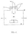
- FIG. 1 depicts apparatus 100 of the invention for pre-treating thermal oxide substrates.
- An exposure chamber 104 houses a chuck 108 which is capable of being heated by a heating device (not shown).
- the chuck 10 8 may be moved in any of 3 dimensions to optimize the exposure of the wafer to the radiation. It is important that radiation be evenly distributed over the surface, as variations in the surface pretreatment can result in variations in the thickness of the subsequently deposited USG film.
- a semiconductor wafer 112 is held on top of the chuck.
- a lamp 116 is disposed within the chamber 104 in any configuration which is suitable for providing even exposure of the wafer to the radiation. In this figure, the lamp 116 is shown on the top of the chamber. Suitable lamps may be any conventional emitter lamps known in the art, including, but not limited to those disclosed in U.S. Patents Nos. 5,432,398 , 5,214,344 , and 5,198,717 .
- the power and exposure times are selected to minimize the surface sensitivity of the USG film deposition.
- the power output of the excimer lamps is in the range of from about 0.005 W/cm 2 to about 100 W/cm 2 .
- the power output is in the range of from about 0.1 W/cm 2 to about 5 W/cm 2 , and more preferably about 1 W/cm 2
- Exposure times can vary inversely with the power output of the generator. However, these exposure guidelines can be altered depending upon the pre-existing state of the surface. For cleaner surfaces, less power and/or shorter exposure durations are necessary.
- the lamp as shown comprises two or more emitter devices 120 which are arranged so as to provide radiation exposure over the wafer surface. Reflective elements 124 reflect the emitted radiation 126 back down into chamber 104 to increase exposure of the wafer to the radiation.
- An inlet port 128 permits the introduction of gas 132 into the exposure chamber 104 .
- the gas 132 is any suitable gas or mixture of gases which do not absorb the wavelengths of excimer radiation produced by lamp 120 . Gases are drawn out of the chamber 104 through an exhaust port 136 . Alternatively, the chamber 104 is evacuated substantially to remove air, and thereby decrease the absorption of radiation 126.
- Table 3 shows some characteristics of lamps. Table 3 Characteristics of UV and VUV Lamps Type Power Range (Watts) Power Density (W/cm 2 ) Max. Radiant Power at ⁇ (W) ⁇ (nm) Max. Irridiance Power at ⁇ (W) ⁇ (nm) Low P Hg 6-150 0.2-0.3 6-45 253.7 200-550 253.7 Low P Hg, Type ABB 1500-2000 10-15 90-500 253.7 2000-6000 253.7 Med.
- An alternative device of this invention for exposing wafers to VUV or UV radiation involves the introduction of the emitter gas directly into the chamber and generating electromagnetic radiation within the chamber without the necessity of enclosing the source in an additional containment vessel, such as a quartz tube.
- This type of process is herein termed an "open emitter” process. It differs from a standard dielectric discharge device described above in that the emitter gas is not enclosed within a separate vessel, but rather, the wafer to be treated is exposed directly to the emitter gas within the chamber.
- the emitter gas flows into the chamber and past an array of electrodes with alternating polarity relative to their neighbors on either side. As electrical charge passes into the electrodes, electrical fields are set up between the electrodes.
- the electrical fields excite the gas, forming, among other species, dimers with high bond energy.
- the excited gas molecules can either emit the photons while above the surface, or may penetrate into the gaps in the device features, where the photon may be emitted. In this way, it is possible to ensure that some UV or VUV radiation reaches the interior of the gaps to exert the desired conditioning effects on the substrate.
- This embodiment also permits the use of emitter gases which generate shorter wavelengths than can conveniently pass through the quartz or other windows in conventional excimer lamps. Such gases include He, Ne and Ar. Additionally, other types of radiation, such as x-rays and electron radiation are useful.
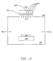
- FIG. 2 depicts a device 200 to treat semiconductor devices with electromagnetic radiation.
- a chamber 204 houses a chuck 208 , which can be heated and is moveable in 3 dimensions.
- a semiconductor wafer 212 is held on chuck 208 , which is positioned under the open emitter device 216 .
- Electrodes 220 are arrayed along one side of the chamber 204.
- Emitter gas 224 is fed in through a port 228 , and flows past electrodes 220 . Alternating current in electrodes 220 excites emitter gas 224 , and the excited gas enters chamber 204 .
- Wafer 212 is exposed to photons 232 , where the pretreatment occurs.
- bias flow for the introduction of other gases is via an inlet port 236 .
- These other gases may be used as emitters, capable of producing wavelengths of radiation different from the first emitter gas. Alternatively, these gases may be used for subsequent conditioning of the wafer while inside the chamber 204 .
- the chamber 204 is evacuated through an exhaust port 240 by a pump (not shown).
- the power and exposure times are selected to minimize the surface sensitivity of the USG film deposition.
- the power output of the emitter lamps is in the range of from about 0.005 W/cm 2 to about 100 W/cm 2 .
- the power output is in the range of from about 0.1 W/cm 2 to about 5 W/cm 2 , and more preferably about 1 W/cm 2
- Exposure times can vary inversely with the power output of the generator. However, these exposure guidelines can be altered depending upon the pre-existing state of the surface. For cleaner surfaces, less power and/or shorter exposure durations are needed.
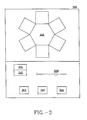
- Figure 3 depicts a tool 300 used for pretreatment and deposition of dielectric films of the invention.
- Wafers to be processed are loaded onto loading stations 304 .
- a robotic arm 308 transfers wafers to a cooling station 312 .
- the pretreatment station 316 contains the electromagnetic radiation emitter devices. Pretreatment station 316 can be similar to the stand alone systems shown in Figure 1 or Figure 2 .
- the robotic arm 308 transfers the wafers to a cluster tool 316 containing multiple deposition stations.
- thermal oxide substrate to the electromagnetic radiation as described above results in decreased surface sensitivity.
- wafers are preferably introduced into equipment containing VUV and/or UV light sources.
- the radiation excites the molecular bonds on the surface of the silicon dioxide substrate, and the undesired bonds are broken, enabling contaminating moieties to leave the surface.
- a first conditioning step involves exposing the wafer to various temperatures and gaseous environments.
- the time of this initial conditioning step is in the range of from about 0 to about 10 minutes, preferably from about 0 seconds to about 3 0 seconds, and more preferably for about 10 seconds.
- the temperatures are from about 25° C to about 700° C, preferably from about 100° C to about 300° C, and more preferably about 200° C.
- the chamber pressure is in the range of about 10 -5 Torr to about 1500 Torr for both the closed and open emitter systems, preferably about 1 Torr to about 100 Torr, and more preferably at about 10 Torr for the closed emitter system.
- preferred pressures are in the range of about 300 Torr to about 900 Torr, and more preferably about 760 Torr.
- the gases are injected into the reaction chamber, and may be heated, cooled, and/or mixed prior to injection, and may also include vaporized chemicals.
- the gases which can be used include inert gases and reactive gases.
- inert gases include He, Ar, Ne, Kr, and Xe.
- reactive gases include NH 3 , chlorofluorocarbons, Cl 2 and HCl, F 2 and derivatives such as SF 6 .
- Br 2 , O 2 and its derivatives such as ozone (O 3 ), H 2 , and gases which can dissociate into Cl, F, Br, O, and S are also useful.
- chemicals which may be injected include HF, HCl, H 2 SO 4 , ClSO 3 , or H 2 O 2 . These materials may be injected alone, or mixed with a carrier has such as nitrogen, hydrogen or oxygen plus any of the inert gases listed above.
- the purpose of the inert gases is to generate the excimer radiation.
- the reactive gases and derivatives of non-reactive gases which, upon exposure to electromagnetic radiation, dissociate and form reactive species, react with the wafer surface to produce a surface with lower surface sensitivity.
- their vapors are injected into the reaction region to dissociate under the electromagnetic radiation, thereby forming reactive moieties.
- the second stage or processing period involves exposure to the electromagnetic energy, preferably in the form of VUV or UV light.
- the exposure period is in the range of from about 10 seconds to about 30 minutes, preferably from about 20 seconds to about 50 seconds, and more preferably about 30 seconds.
- This step may be repeated for up to several times at either the same or different conditions of temperature, pressure, and environmental gas conditions.
- the radiation used is usually in the range of about 100 nanometers (nm) to about 450 nm, preferably from about 123 nm to about 225 nm, and more preferably about 147 nm to 172 nm. It is also possible to use radiation of shorter wavelengths, which includes x-ray and electron sources which generate radiation with wavelengths below 100 nm.
- any reasonable power density can be used which does not cause excess damage to the electronic devices.
- the most useful power densities are in the range of about 0.005 W/cm 2 to about 100 W/cm 2 , preferably about 0.1 W/cm 2 to about 5 W/cm 2 , and more preferably about 1 W / cm 2 .
- Post conditioning steps can be used to maintain the desired surface conditions for extended periods of time up to and including about 2 weeks.
- Post-conditioning processes can be performed using various combinations of temperature, chamber pressure, and gas environment. Any of the above gases or mixtures of gases can be used, preferably including oxygen, nitrogen, and/or ammonia.
- a gaseous environment permits the attachment of ionic species to the surface of the wafer, rendering it neutral to absorption of contaminants removed during the treatment. For example, ammonia which upon heating to 400° C for the TEOS ozone deposition, would be released from the surface., exposing the underlying surface with the low surface sensitivity.
- Deposition of USG films is accomplishes by standard methods in the art. Deposition methods commonly use chemical vapor deposition (CVD) and transport polymerization (TP). Typically, a cap layer of silicon nitride (Si 3 N 4 ) may optionally be applied over portions of the thermal oxide layer, prior to depositing a TEOS ozone film. Using these processes, precursors such as TEOS and ozone are reacted together to form reactive intermediates molecules, which can then polymerize to form the USG film.
- the flow rate of TEOS is in the range of about 0.05 gm/min. to about 1.5 gm/min, and preferably about 0.15 to about 0.4 gm/min.
- the ozone concentration should be in the range of about greater than 0 % to about 18% by volume, preferably in the range of about 5% and 12 % by volume.
- the deposition temperature can be in the range of about 100° C and about 600° C, and preferably about 400° C. Under these conditions, the rates of deposition of USG on pre-treated thermal oxide are nearly identical to the rates of deposition of USG on bare silicon. Thus, the concentration of ozone which can be used in the deposition of the layer can be increased to over 6 volume % without compromising the rate of deposition of the USG film.
- the physical-chemical processes of this invention have desired effects on film manufacture.
- the rates of deposition on untreated thermal oxide are considerably lower than on bare silicon. Rates as low as 500 ⁇ per minute are not uncommon using standard TEOS and ozone concentrations.
- Radiation pre-treatment increases the rate of TEOS deposition on thermal oxide substrates to rates comparable to those on bare silicon. After radiation pre-treatment, the TEOS deposition rates are often greater than about 2000 ⁇ per minute, and can reach about 5000 ⁇ per minute.
- the film can be annealed by heating to about 900° C in nitrogen atmosphere for a few minutes, preferably for about 30 minutes. This annealing step is known to increase the density of the USG layer, reducing the water content of the film, and thereby conferring more desirable dielectric and mechanical properties to the film
- the surface pre-treatment results in a much more even distribution of USG.
- the final surface roughness of the deposited USG film is in the range below about 10 ⁇ , and preferably is between about 2 ⁇ and 8 ⁇ root mean square deviation from planarity.
- an ozone film can be deposited, in which the ozone concentration is in the range of from about 0.5 volume % to about 18 volume %, preferably in the range of from about 5 volume % to about 12 volume %.
- Depositing USG under these ranges of ozone concentration results in films with more desirable surface qualities.
- the increased deposition rates increase the efficiency of gap filling, thus, enabling the production of semiconductor devices with high device density and good electrical insulation.
- pre-treating the thermal oxide surface with electromagnetic radiation enables the deposition of a flow-like film at low temperatures, which actually fills the gaps better than does a conformal film.
- the desired gap filing properties of the high ozone USG films are obtainable using the UV/VUV pretreatment process of this invention at temperatures of about 400° C.
- the advantage of this invention over the prior art is that with flow-like deposition, there is no weak seam in the middle of the gap, and therefore, there is less degradation of device performance and increased device reliability.
- particle deposition is minimized, as is the consumption of chemicals by depositing at 400° C.
Description
- The field of the invention comprises methods for manufacturing semiconductor devices.
- For the past 20 years, the integrated circuit (IC) device density has doubled about every 18 months. As device density increases, the space between semiconductor device features must therefore decrease. However, as the space between device features decreases, the ability to electrically isolate the devices becomes more diffcult. To provide the electrical isolation as well as mechanical structure to fabricate the devices, the narrow spaces are filled with silicon dioxide or other suitable insulator. To separate the devices within the silicon substrate, spaces are provided by means of shallow trenches. These trenches are filled with silicon dioxide which can be derived from the reaction of tetraethylorthosilicate (TEOS) and ozone.
- The fabrication of shallow trenches is currently carried out by providing a semiconductor substrate, typically silicon wafer with a thermal oxide surface, which is manufactured by exposing a surface of silicon to an oxidizing agent such as oxygen at high temperatures to create a surface of SiO2.
- Similarly, polysilicon interconnect layers as well as conductive metal interconnects have spaces which are to be filled with silicon dioxide or other suitable dielectric material to insulate the conductive layers from each other. The dielectric material, such as SiO2, can be made of un-doped silicate glass (USG) or non-doped silicon glass (NSG). These terms are considered to be equivalent in this application. USG is deposited using the precursors, TEOS and ozone, using a chemical vapor deposition (CVD) processing.
- Conventionally deposited films of USG based on TEOS/ozone technology, however, have several drawbacks. Of these, one of the most important is the sensitivity of the deposited film to the condition of the substrate on which the film is deposited. This is termed "surface sensitivity." {See Kwok et al., J. Electrochem. Soc., 141(8):2172-2177 (1994); Matsuura et al., Proceedings of the 22d International Conference on Solid State Devices and Materials, Sendai, pp:239-242 (1990); Fujino et al., J. Electrochem. Soc. 138(2):550-554 (1991); and Fujino et al., J. Electrochem. Soc. 139(6):1690-1692 (1992)} Surface sensitivity is characterized by inconsistent and variable deposition rates and increased roughness of the resulting films as the process conditions are varied. The process conditions of interest are deposition temperature, deposition pressure, mole-fraction of the reactants (e.g., TEOS and ozone), and possibly some hardware conditions specific to the design of the reactor used to deposit these films.
- Increasing the ozone concentration can affect the deposition rate and increased surface roughness, as reflected both in direct measurements of surface features using scanning electron microscopy, as well as increased wet etching rates observed with aqueous HF solutions. One possible hypothesis to account for surface roughness is the nucleation mechanism, also known as an "island growth mechanism" originating on the surfaces being covered. Depending on the molecular makeup of the surface and its state, the TEOS ozone begins deposition in a granular form. As the film becomes thicker, this granular structure can be seen as surface roughness. This is in contrast with a smooth, "layered growth mechanism" which results in an even, smooth layer of deposited material.
- Surface roughness introduces a number of adverse effects for processing the TEOS ozone films and films subsequently deposited on the TEOS ozone films. As photoresist is coated on the wafer surface to form holes (vias) for interconnecting conductive layers, the photoresist's surface adhesion is decreased on rough surfaces. With the exposure of the photoresist to the stepper light radiation, the granular surface introduces many reflections resulting in poor dimensional definition of the photoresist layer. During etching, the granular surface reduces adhesion with the possibility of delamination of the photoresist layer.
- Surface sensitivity is observed for several types of substrates, including silicon dioxide formed either as thermal oxide, or as SiO2 deposited through TEOS ozone or TEOS oxygen plasma processes (PECVD). The SiO2 can be either phosphorous doped silicate glass (PSG), spin on glass (SOG), borophosphorous silicate glass (BSG), or combinations of PSG and BSG. Additionally, surface sensitivity can be a problem for dielectric layers deposited on silicon nitride (Si3N4).
- Thus, the semiconductor industry is interested in decreasing the effects of surface sensitivity and ensuring good gap filling with high quality dielectric materials. However, to date the problems of surface sensitivity and poor gap filling have been not been adequately addressed.
- Several approaches have been used to treat semiconductor surfaces.
-
Maeda et al. U.S. Patent No. 5,484,749 described a process whereby semiconductor devices were exposed to heat and high frequency plasma to treat the surface of an SiO2 layer prior to deposition of a TEOS ozone film. However, this process requires additional costly plasma treatment equipment. -
EP 0445535 discloses a method of forming an oxide film in an environment containing an inert gas and an oxidising gas and a method of manufacturing an electronic device utilizing this oxide film, where the inert gas/oxidising gas environment prevents fixed electrical charges from being generated on the film. -
US 5225355 discloses a gettering treatment process comprises the step of irradiating an ultraviolet light onto an insulating layer (a silicon oxide thin layer formed by thermally oxidizing silicon), in a chlorine-containing gas atmosphere. The ultraviolet light excites and dissociates the chlorine-containing gas thereby to generate chlorine radicals which uniformly penetrate the insulating layer, and serve to trap metal impurities within the silicon oxide thin layer. -
EP 0171605 discloses a method of manufacturing a semiconductor integrated circuit wherein a thin film such as insulator film is formed on selected areas of a semiconductor substrate. This is achieved by placing a photoresist on selected areas of the semiconductor substrate in advance, such that the film is deposited only on the parts other than the photoresist. - Another approach by
Maeda et al, U.S. Patent No. 5,051,380 was to deposit the - USG film discontinuously. A first layer of USG is deposited using a low ozone concentration, and then a subsequent USG film is deposited using a higher ozone concentration. However, USG films using low ozone concentration have less desirable film qualities, such as high water content and absorption, high etch rates, and shrinkage during high temperature annealing, which induces stress and formation of voids or seams. {Kwok et al., J. Electrochem. Soc. 141 (8):2172-2177 (1994).) Furthermore, the thickness needed to overcome surface sensitivity of a low ozone USG film may be as great as 100nm (1000 Å), thus filling the gap with poor quality oxide and preventing filling the gap with high quality, highozone oxide. As gaps decrease to 0.25 µm, after a first layer of a low ozone USG film, only 50nm (500 Å) would be available for a second layer of a effective high ozone USG material to fill the gaps.
- An additional approach is to modify the surface of the USG film.
Maeda et al., U.S. Patent No. 5,387,546 taught the exposure of deposited semiconductor films to ultraviolet radiation during heating. The ultraviolet radiation was produced by a mercury lamp which generates electromagnetic radiation with wavelengths of 185 nanometers (nm) and 254 nm, as well as some longer wavelength radiation. However, because this process is carried out on layers of USG film which have already been deposited, it does not deal with the problem of surface sensitivity. Thus, there is a need for improved ways of reducing surface sensitivity. - On the basis of the foregoing, one object of the invention is to provide a method for decreasing the surface sensitivity of semiconductor wafer surfaces which are covered with dielectric films.
- Another object is to decrease surface sensitivity without adversely affecting the rates of deposition of dielectric films and conductive.
- The invention includes methods for pre-treating semiconductor surfaces to reduce the surface sensitivity of the film.
- Therefore, one aspect of this invention is the development of methods for exposing thermal oxide substrates to electromagnetic radiation in the vacuum ultraviolet wavelengths to reduce the surface sensitivity of subsequently deposited dielectric films.
- Another aspect of this invention is the development of methods for reducing surface sensitivity while maintaining desired rates of deposition of thin dielectric films.
- These and other features and advantages of the present invention will be apparent from the Detailed Description of the Invention in conjunction with the Figures, and Claims.
-
-
Figure 1 is a depiction of an embodiment of the invention for exposing semiconductor wafers to electromagnetic radiation derived from a dielectric barrier discharge device. -
Figure 2 is a depiction of an embodiment of the invention for exposing semiconductor wafers to electromagnetic radiation derived from an open emitter apparatus. -
Figure 3 is a depiction of an embodiment of the invention including a tool for processing semiconductor wafers which includes a structure for exposing wafers to electromagnetic radiation. - The Figures are more thoroughly explained in the Detailed Description of the Invention.
- The present invention comprises methods and apparatus for pre-treating semiconductor substrates with electromagnetic radiation of vacuum ultraviolet wavelengths prior to the deposition of semiconductor dielectric layers. This pretreatment substantially reduces the surface sensitivity of the deposition process so that thermal oxide surfaces can have layers of dielectric material deposited thereon at higher rates and with surface smoothness nearly identical to the surface smoothness of dielectric materials deposited on bare silicon. Moreover, the quality of the USG film is high, providing better dielectric properties and permitting effective electrical insulation and the filling of gaps in the 0.25 µm range.
- This invention is rooted in the recognition that surface sensitivity is determined by the nature of the substrate surface. The nature of the surface is determined at least partially by the atomic and molecular species and how they are bonded together on the substrate surface. The substrate material, the methods by which it is prepared, and the ambient conditions to which it is exposed prior to dielectric deposition, are factors that influence the nature of the surface and the quality of the subsequently deposited film.
- There are several theories which may account for surface sensitivity. One theory is that surface sensitivity is related to the wetting behavior of the substrate. A pure silicon surface is hydrophobic, (that is, it repels water), whereas thermal oxide, made by exposing a silicon surface to oxygen at elevated temperatures, is hydrophilic, (that is, water wets the surface). This theory therefore states that the surface sensitivity is related to the hydrophilicity of the substrate.
- A second theory relates to the electrostatic interaction between the substrate surface and the deposited species. {Kwok et al., J. Electrochem. Soc. 141(8):2172-2177 (1994)} It is observed that even on silicon wafers, USG deposited with high ozone concentrations shows surface sensitivity if fluorine atoms are present instead of hydrogen. The deposition of TEOS and ozone takes place through the formation of an intermediate species, hypothesized to be electronegative, in the gas phase. Because fluorine is extremely electronegative, this gas phase intermediate may be repelled by fluorine atoms on the surface. This results in low deposition rates and uneven deposition. According to this theory, unlike fluorine atoms, hydrogen atoms are not very electronegative, so deposition of intermediates on substrates free of fluorine is more rapid and more even.
- A third theory relates to the presence of undesirable types of silicon bonds on the surface. For example, the thermal oxide surface is expected to have Si-O-Si, Si-H, and Si-OH bonds on the surface along with some hydrocarbon or other organic contaminants. According to this theory, the presence of these types of bonds decreases the homogeneity of the resulting film, thereby causing it to have a rough surface. According to this theory, these bonds may form when contaminants on the surface bind to the silicon or oxygen atoms in the SiO2 film.
- A fourth theory relates to the presence of organic contaminants on the substrate surface. Typical sources of organic contamination are clean room air and the photoresist residue from photolithography processes. The organic moieties found include silicon carbide, amides, silicones, organophosphorous compounds, C6 - C28 aliphatic or aromatic hydrocarbons, phthalates, alcohols (e.g., isopropyl alcohol), N-methyl pyrrolidone, creosols and amines. Camenaind et al., Balazs News, Number 20: 1-3 (October 1997); and Camenzind et al., MICRO pp: 71-76 (October 1995).
- These theories are included only for descriptive purposes, and the present invention does not rely upon any particular of these theories for its operability. Furthermore, other theories may account for surface sensitivity. Regardless of the molecular source or mechanism responsible for surface sensitivity, the present invention uses electromagnetic radiation preferably in the ultraviolet and vacuum ultraviolet ranges to prepare the surface prior to deposition of the layer, preferably a dielectric layer.
- According to some theories, surface modification requires the breaking of undesirable bonds and/or the formation of desirable surface bonds or surface sites. These bonds include Si-OH, Si-C, Si-N, among others. The bond energies of some relevant bonds are shown in Table 1. These energies lie in the visible, ultraviolet (UV) and vacuum ultraviolet (VUV) range, and therefore electromagnetic radiation of these wavelengths will interact with these bonds. Therefore, it is possible to modify the bonding state of the thermal oxide surface by exposing this surface to UV or VUV radiation.
Table 1 Bond Energies For Selected Bond Bond Energy (eV) Wavelength (nm) H-H 4.52 274 C-C 3.60 344 Si-Si 1.83 678 N-N 1.67 745 O-O 1.44 861 C-H 4.28 289 Si-H 3.05 406 N-H 4.05 306 O-H 4.80 259 C-Si 3.01 413 C-N 3.02 410 C-O 3.64 340 Si-O 3.82 324 C=C 6.34 195 C≡C 9.22 134 - As can be seen from Table 1, certain bonds can absorb electromagnetic radiation and thereby be disrupted. With the dissociation of these undesirable bonds, the contaminating moieties can be removed from the surface. The electromagnetic radiation has sufficient energy to break the bonds, thereby allowing removal of the moieties from the surface.
- Mercury-vapor lamps, hydrogen lamps, lasers, and the dielectric barrier discharge lamps including excimer radiation devices are a few different devices useful for obtaining the UV and VUV radiation of this invention. With recent advances in dielectric barrier discharge technology, it is now possible to make UV and VUV lamps that can provide reasonably high intensity monochromatic radiation over a large surface area. These types of lamps are therefore suitable for practicing this invention. However, because it is possible to use any source of UV and VUV radiation, some aspects of the invention are not limited to any particular source of radiation.
- Excimer devices are characterized by the use as emitter moieties, atoms which under normal temperatures and other conditions do not form chemical bonds between them. For example, noble gases normally do not form interatomic bonds. However, under high energy conditions, noble gases can form dimers. When these dimers break down, the energy of the bonds is released as high energy electromagnetic radiation. Depending on what the excimer gas is, the wavelength of the emitted radiation may be in the ultraviolet or vacuum ultraviolet range.
- The bonds shown in Table 1 correspond to energies in the UV and VUV ranges. Several types of devices are capable of generating electromagnetic radiation in the wavelength ranges needed. VUV or UV radiation can be provided by dielectric barrier or silent discharge equipment using a variety of gases or gas mixtures according to methods known in the art. VUV and UV radiation can be generated from noble gases and other atomic species (see Table 2).
Table 2 Emission Wavelengths For Selected Electromagnetic Radiation Emitters Emitter Moiety Wavelength (nanometers) He2 60-100 Ne2 80-90 Ar2 107-165 Kr2 140-160 Xe2 160-190 N2 337-415 KrF 240-255 Hg/Ar 235 Deuterium 150 - 250 XeF 340 - 360, 400 - 550 XeCl 300-320 XeI 240-260 ArF 180-200 ArCl 165-190 ArCl/KrCl 165 - 190, 200 - 240 KrCl 200-240 Hg 185, 254, 320 - 370, 390 - 420 Se 196, 204, 206 - Data from Eliasson et al.,
U.S. Patent No. 4,983,881 and Kogelsehatz,U.S. Patent No. 5,432,398 . - These ranges of wavelengths encompass the wavelengths equivalent to the energy of the undesired bonds on the substrate surface. Although the wavelengths above are those exhibiting the maximum power, there is a bandwidth of the wavelengths generated by each of the above emitter moieties. The bandwidths vary from about 1 to about 17 nm. {Newman et al., Aust. J. Phys. 48:543-556 (1995), } Thus, these emitters can be used to expose the surface of a semiconductor substrate to a spectrum of electromagnetic radiation, thereby increasing the number and types of chemical bonds which may be dissociated.
- Dielectric barrier discharge devices, also known as silent discharge devices, consist of two conductive plates, each covered with a dielectric layer and are separated from each other by an emitter gas-containing gap. Examples of such emitter gases are shown in Table 2. The dielectric barrier decreases the conduction through the gap, and therefore, the generation of current flow between the plates requires a higher voltage. When the voltage is sufficient to overcome the resistance of the dielectric materials, the resulting current through the gas is substantially higher than without the dielectric layer, and consequently, more power is delivered to the gas. When the dielectric breakdown occurs, small microplasmas are formed across the gap. The current excites the gas and the resulting photons emitted are in the desired VUV and UV ranges, depending on which atomic species are present in the gas. In the excimer process, the microplasmas deliver the energy to the gases inducing the formation of dimers. As these dimers dissociate, the excimer radiation is emitted. When emitted within the exposure chamber, these photons are directed at the surface of the wafer, and interact with molecules on the surface, decreasing the surface sensitivity to subsequently deposited USG films.
- A subset of useful lamps include dielectric barrier excimer lamps. Excimer lamps are known in the art, and are exemplified by the devices described in
Kogelschatz, U.S. Patent No. 5,432,398 ;Kogelschatz, U.S. Patent No. 5,386,170 ;Eliasson et al., U.S. Patent No. 4,837,484 ;Eliasson et al., U.S. Patent No. 4,945,290 ;Eliasson et al., U.S. Patent No. 4,983,881 ;Gellert et al., U.S. Patent No. 5,006,758 ;Kogelschatz et al., U.S. Patent No. 5,198,717 ;Kogelschatz, U.S. Patent No. 5,214,344 ; andKogelschatz, U.S. Patent No. 5,386,170 . - Any suitable lamp is useful for practicing the method of this invention. These devices comprise a central electrode surrounded by a quartz dielectric. Surrounding the quartz dielectric is a chamber containing the emitter gas, such as Xe or those exemplified by Table 2. Surrounding the chamber containing the emitter gas, another dielectric shield, transparent to the UV or VUV wavelengths generated encloses the gas in the tube. Suitable materials include, but are not limited to quartz, LiF, MgF2, or CaF2. An outer electrode, commonly of mesh wire, surrounds the outer dielectric layer.
- Excitation of the emitter gas results in the production of electromagnetic radiation which exits the tube inside the exposure chamber. Because air in the chamber may absorb the photons preventing them from reaching the substrate surface, the exposure chamber is either evacuated or the air is replaced with a gas which does not absorb the wavelength of radiation produced by the emitter device. For a xenon excimer device, suitable gases include nitrogen, argon, helium, xenon or ammonia. For other emitter devices, non-absorbing gases are chosen accordingly to permit passage of the photons to the substrate surface.
-
Figure 1 depictsapparatus 100 of the invention for pre-treating thermal oxide substrates. Anexposure chamber 104 houses achuck 108 which is capable of being heated by a heating device (not shown). Thechuck 108 may be moved in any of 3 dimensions to optimize the exposure of the wafer to the radiation. It is important that radiation be evenly distributed over the surface, as variations in the surface pretreatment can result in variations in the thickness of the subsequently deposited USG film. Asemiconductor wafer 112 is held on top of the chuck. Alamp 116 is disposed within thechamber 104 in any configuration which is suitable for providing even exposure of the wafer to the radiation. In this figure, thelamp 116 is shown on the top of the chamber. Suitable lamps may be any conventional emitter lamps known in the art, including, but not limited to those disclosed inU.S. Patents Nos. 5,432,398 ,5,214,344 , and5,198,717 . - The power and exposure times are selected to minimize the surface sensitivity of the USG film deposition. The power output of the excimer lamps is in the range of from about 0.005 W/cm2 to about 100 W/cm2. Preferably, the power output is in the range of from about 0.1 W/cm2 to about 5 W/cm2, and more preferably about 1 W/cm2 Exposure times can vary inversely with the power output of the generator. However, these exposure guidelines can be altered depending upon the pre-existing state of the surface. For cleaner surfaces, less power and/or shorter exposure durations are necessary.
- The lamp as shown comprises two or
more emitter devices 120 which are arranged so as to provide radiation exposure over the wafer surface.Reflective elements 124 reflect the emittedradiation 126 back down intochamber 104 to increase exposure of the wafer to the radiation. Aninlet port 128 permits the introduction ofgas 132 into theexposure chamber 104. Thegas 132 is any suitable gas or mixture of gases which do not absorb the wavelengths of excimer radiation produced bylamp 120. Gases are drawn out of thechamber 104 through anexhaust port 136. Alternatively, thechamber 104 is evacuated substantially to remove air, and thereby decrease the absorption ofradiation 126. - Any of several lamps are suitable for this invention. Table 3 shows some characteristics of lamps.
Table 3 Characteristics of UV and VUV Lamps Type Power Range (Watts) Power Density (W/cm2) Max. Radiant Power at λ (W) λ (nm) Max. Irridiance Power at λ (W) λ (nm) Low P Hg 6-150 0.2-0.3 6-45 253.7 200-550 253.7 Low P Hg, Type ABB 1500-2000 10-15 90-500 253.7 2000-6000 253.7 Med. P Hg 75-60,000 40-300 1.5-3500 254 700-5000 254 Fusion 6000 240 270 201-250 28,000 201-250 Type H 500 50,000 251-300 335 251-300 35,000 301-350 301-350 XeCl 10,000 50 330 308 11,700 308 KrCl 10,000 50 330 222 11,700 222 Xe 10,000 50 240 172 8500 172 - An alternative device of this invention for exposing wafers to VUV or UV radiation involves the introduction of the emitter gas directly into the chamber and generating electromagnetic radiation within the chamber without the necessity of enclosing the source in an additional containment vessel, such as a quartz tube. This type of process is herein termed an "open emitter" process. It differs from a standard dielectric discharge device described above in that the emitter gas is not enclosed within a separate vessel, but rather, the wafer to be treated is exposed directly to the emitter gas within the chamber. The emitter gas flows into the chamber and past an array of electrodes with alternating polarity relative to their neighbors on either side. As electrical charge passes into the electrodes, electrical fields are set up between the electrodes. The electrical fields excite the gas, forming, among other species, dimers with high bond energy. The excited gas molecules can either emit the photons while above the surface, or may penetrate into the gaps in the device features, where the photon may be emitted. In this way, it is possible to ensure that some UV or VUV radiation reaches the interior of the gaps to exert the desired conditioning effects on the substrate. This embodiment also permits the use of emitter gases which generate shorter wavelengths than can conveniently pass through the quartz or other windows in conventional excimer lamps. Such gases include He, Ne and Ar. Additionally, other types of radiation, such as x-rays and electron radiation are useful.
-
Figure 2 depicts adevice 200 to treat semiconductor devices with electromagnetic radiation. Achamber 204 houses achuck 208, which can be heated and is moveable in 3 dimensions. Asemiconductor wafer 212 is held onchuck 208, which is positioned under theopen emitter device 216.Electrodes 220 are arrayed along one side of thechamber 204.Emitter gas 224 is fed in through aport 228, and flowspast electrodes 220. Alternating current inelectrodes 220 excitesemitter gas 224, and the excited gas enterschamber 204.Wafer 212 is exposed tophotons 232, where the pretreatment occurs. Optionally, bias flow for the introduction of other gases is via aninlet port 236. These other gases may be used as emitters, capable of producing wavelengths of radiation different from the first emitter gas. Alternatively, these gases may be used for subsequent conditioning of the wafer while inside thechamber 204. Thechamber 204 is evacuated through anexhaust port 240 by a pump (not shown). - The power and exposure times are selected to minimize the surface sensitivity of the USG film deposition. The power output of the emitter lamps is in the range of from about 0.005 W/cm2 to about 100 W/cm2. Preferably, the power output is in the range of from about 0.1 W/cm2 to about 5 W/cm2, and more preferably about 1 W/cm2 Exposure times can vary inversely with the power output of the generator. However, these exposure guidelines can be altered depending upon the pre-existing state of the surface. For cleaner surfaces, less power and/or shorter exposure durations are needed.
-
Figure 3 depicts atool 300 used for pretreatment and deposition of dielectric films of the invention. Wafers to be processed are loaded onto loadingstations 304. Arobotic arm 308 transfers wafers to acooling station 312. Thepretreatment station 316 contains the electromagnetic radiation emitter devices.Pretreatment station 316 can be similar to the stand alone systems shown inFigure 1 orFigure 2 . After pretreatment, therobotic arm 308 transfers the wafers to acluster tool 316 containing multiple deposition stations. - Exposing thermal oxide substrate to the electromagnetic radiation as described above results in decreased surface sensitivity. To perform such exposure, wafers are preferably introduced into equipment containing VUV and/or UV light sources. According to at least one theory, the radiation excites the molecular bonds on the surface of the silicon dioxide substrate, and the undesired bonds are broken, enabling contaminating moieties to leave the surface.
- The typical process includes three stages. A first conditioning step involves exposing the wafer to various temperatures and gaseous environments. The time of this initial conditioning step is in the range of from about 0 to about 10 minutes, preferably from about 0 seconds to about 3 0 seconds, and more preferably for about 10 seconds. The temperatures are from about 25° C to about 700° C, preferably from about 100° C to about 300° C, and more preferably about 200° C. The chamber pressure is in the range of about 10-5 Torr to about 1500 Torr for both the closed and open emitter systems, preferably about 1 Torr to about 100 Torr, and more preferably at about 10 Torr for the closed emitter system. For the open emitter system, preferred pressures are in the range of about 300 Torr to about 900 Torr, and more preferably about 760 Torr. The gases are injected into the reaction chamber, and may be heated, cooled, and/or mixed prior to injection, and may also include vaporized chemicals.
- The gases which can be used include inert gases and reactive gases. Examples of inert gases include He, Ar, Ne, Kr, and Xe. Examples of reactive gases include NH3, chlorofluorocarbons, Cl2 and HCl, F2 and derivatives such as SF6. Additionally, Br2, O2 and its derivatives such as ozone (O3), H2, and gases which can dissociate into Cl, F, Br, O, and S are also useful. Examples of chemicals which may be injected include HF, HCl, H2SO4, ClSO3, or H2O2. These materials may be injected alone, or mixed with a carrier has such as nitrogen, hydrogen or oxygen plus any of the inert gases listed above.
- The purpose of the inert gases is to generate the excimer radiation. The reactive gases and derivatives of non-reactive gases which, upon exposure to electromagnetic radiation, dissociate and form reactive species, react with the wafer surface to produce a surface with lower surface sensitivity. In the case of the chemicals, their vapors are injected into the reaction region to dissociate under the electromagnetic radiation, thereby forming reactive moieties.
- The second stage or processing period involves exposure to the electromagnetic energy, preferably in the form of VUV or UV light. The exposure period is in the range of from about 10 seconds to about 30 minutes, preferably from about 20 seconds to about 50 seconds, and more preferably about 30 seconds. This step may be repeated for up to several times at either the same or different conditions of temperature, pressure, and environmental gas conditions. The radiation used is usually in the range of about 100 nanometers (nm) to about 450 nm, preferably from about 123 nm to about 225 nm, and more preferably about 147 nm to 172 nm. It is also possible to use radiation of shorter wavelengths, which includes x-ray and electron sources which generate radiation with wavelengths below 100 nm.
- Any reasonable power density can be used which does not cause excess damage to the electronic devices. The most useful power densities are in the range of about 0.005 W/cm2 to about 100 W/cm2, preferably about 0.1 W/cm2 to about 5 W/cm2, and more preferably about 1 W/cm2.
- Post conditioning steps can be used to maintain the desired surface conditions for extended periods of time up to and including about 2 weeks. Post-conditioning processes can be performed using various combinations of temperature, chamber pressure, and gas environment. Any of the above gases or mixtures of gases can be used, preferably including oxygen, nitrogen, and/or ammonia. A gaseous environment permits the attachment of ionic species to the surface of the wafer, rendering it neutral to absorption of contaminants removed during the treatment. For example, ammonia which upon heating to 400° C for the TEOS ozone deposition, would be released from the surface., exposing the underlying surface with the low surface sensitivity.
- Deposition of USG films is accomplishes by standard methods in the art. Deposition methods commonly use chemical vapor deposition (CVD) and transport polymerization (TP). Typically, a cap layer of silicon nitride (Si3N4) may optionally be applied over portions of the thermal oxide layer, prior to depositing a TEOS ozone film. Using these processes, precursors such as TEOS and ozone are reacted together to form reactive intermediates molecules, which can then polymerize to form the USG film. The flow rate of TEOS is in the range of about 0.05 gm/min. to about 1.5 gm/min, and preferably about 0.15 to about 0.4 gm/min. The ozone concentration should be in the range of about greater than 0 % to about 18% by volume, preferably in the range of about 5% and 12 % by volume. The deposition temperature can be in the range of about 100° C and about 600° C, and preferably about 400° C. Under these conditions, the rates of deposition of USG on pre-treated thermal oxide are nearly identical to the rates of deposition of USG on bare silicon. Thus, the concentration of ozone which can be used in the deposition of the layer can be increased to over 6 volume % without compromising the rate of deposition of the USG film.
- The physical-chemical processes of this invention have desired effects on film manufacture. First, because contaminants are removed from the thermal oxide surface, the rate of deposition, of USG films is increased, compared to the deposition on untreated thermal oxide alone. The rates of deposition on untreated thermal oxide are considerably lower than on bare silicon. Rates as low as 500 Å per minute are not uncommon using standard TEOS and ozone concentrations. Radiation pre-treatment increases the rate of TEOS deposition on thermal oxide substrates to rates comparable to those on bare silicon. After radiation pre-treatment, the TEOS deposition rates are often greater than about 2000 Å per minute, and can reach about 5000 Å per minute.
- After deposition, the film can be annealed by heating to about 900° C in nitrogen atmosphere for a few minutes, preferably for about 30 minutes. This annealing step is known to increase the density of the USG layer, reducing the water content of the film, and thereby conferring more desirable dielectric and mechanical properties to the film
- Moreover, the surface pre-treatment results in a much more even distribution of USG. The final surface roughness of the deposited USG film is in the range below about 10 Å, and preferably is between about 2 Å and 8 Å root mean square deviation from planarity.
- Furthermore, an ozone film can be deposited, in which the ozone concentration is in the range of from about 0.5 volume % to about 18 volume %, preferably in the range of from about 5 volume % to about 12 volume %. Depositing USG under these ranges of ozone concentration results in films with more desirable surface qualities. Moreover, the increased deposition rates increase the efficiency of gap filling, thus, enabling the production of semiconductor devices with high device density and good electrical insulation.
- One possible reason for the improved gap filling is that without pretreatment, the uneven distribution of USG on the gap sidewalls may create barriers to the penetration of reactive intermediates into the gap, thereby decreasing further deposition within the gap. By creating a more even deposition of USG on the sidewall surfaces of the gaps, there will be less opportunity for barriers to form, and therefore, there will be less hindrance to the diffusion of intermediates into the gaps. As the intermediates continue to flow into the gaps, the deposition of the final TEOS ozone film will continue until the gap is completely filled.
- Prior methods of filling gaps have focused upon the deposition of a flow-like film within the gap. These prior methods have found that higher temperatures, around 500° C, produce conformal films of high ozone USG. However, as a conformal layer films a gap, the area in the middle of the gap can be the site of formation of a "weak seam," or an area of poor quality film where the two sides of the conformal film converge. This type of void degrades device performance and may result in trapping of contaminants which can decrease device reliability. Moreover, high temperature deposition results in deposition of articles and increases the consumption of chemicals.
- Unexpectedly, we have found that pre-treating the thermal oxide surface with electromagnetic radiation enables the deposition of a flow-like film at low temperatures, which actually fills the gaps better than does a conformal film. The desired gap filing properties of the high ozone USG films are obtainable using the UV/VUV pretreatment process of this invention at temperatures of about 400° C. The advantage of this invention over the prior art is that with flow-like deposition, there is no weak seam in the middle of the gap, and therefore, there is less degradation of device performance and increased device reliability. Moreover, particle deposition is minimized, as is the consumption of chemicals by depositing at 400° C.
- This is only one possible theory to account for the improved gap filling of the present invention, and we do not rely upon this or any other particular theory of operability. Other theories may account for the observations, and an are considered to be part of this invention.
Claims (3)
- A method for preparing a surface of a semiconductor wafer, comprising:providing a semiconductor wafer, wherein the surface of said wafer has a layer of dielectric material thereon, characterised byexposing the surface of the wafer to electromagnetic radiation in the range of vacuum ultraviolet wavelengths of 147nm to 172nm, 123nm to 225nm, or below 100nm sufficient to reduce the inconsistent and variable deposition rates and increased roughness of a subsequently deposited film onto said semiconductor wafer.
- The method of claim 1, wherein the dielectric material is selected from the group consisting of thermal oxide, silicon dioxide deposited by plasma enhanced chemical vapor deposition, silicon dioxide deposited by high density plasma enhanced chemical vapor deposition, phosphorous silicate glass, borophosphorous silicate glass, spin on glass, BSG, a tetraethylorthosilicate (TEOS) ozone film and silicon nitride.
- A semiconductor wafer, wherein the surface of said semiconductor wafer comprises a thermal oxide layer and wherein said surface of said semiconductor wafer has been prepared by exposing said surface to vacuum ultraviolet radiation sufficient to reduce inconsistent and variable deposition rates and increased roughness of a subsequently deposited un-doped silicate glass (USG) film onto said surface of said semiconductor wafer, and wherein the surface roughness of the deposited USG film is in the range between 0,2nm (2Å) and 0,8nm (8Å) root mean square deviation from planarity.
Applications Claiming Priority (3)
| Application Number | Priority Date | Filing Date | Title |
|---|---|---|---|
| US08/986,916 US6015759A (en) | 1997-12-08 | 1997-12-08 | Surface modification of semiconductors using electromagnetic radiation |
| US986916 | 1997-12-08 | ||
| PCT/US1998/024998 WO1999030353A1 (en) | 1997-12-08 | 1998-11-19 | Surface modification of semiconductors using electromagnetic radiation |
Publications (3)
| Publication Number | Publication Date |
|---|---|
| EP1038307A1 EP1038307A1 (en) | 2000-09-27 |
| EP1038307A4 EP1038307A4 (en) | 2005-01-05 |
| EP1038307B1 true EP1038307B1 (en) | 2013-09-11 |
Family
ID=25532874
Family Applications (1)
| Application Number | Title | Priority Date | Filing Date |
|---|---|---|---|
| EP98960398.0A Expired - Lifetime EP1038307B1 (en) | 1997-12-08 | 1998-11-19 | Surface modification of semiconductors using electromagnetic radiation |
Country Status (7)
| Country | Link |
|---|---|
| US (1) | US6015759A (en) |
| EP (1) | EP1038307B1 (en) |
| JP (1) | JP2002502108A (en) |
| KR (1) | KR100672066B1 (en) |
| AU (1) | AU1600399A (en) |
| TW (1) | TW445527B (en) |
| WO (1) | WO1999030353A1 (en) |
Families Citing this family (49)
| Publication number | Priority date | Publication date | Assignee | Title |
|---|---|---|---|---|
| US6124211A (en) * | 1994-06-14 | 2000-09-26 | Fsi International, Inc. | Cleaning method |
| US7025831B1 (en) | 1995-12-21 | 2006-04-11 | Fsi International, Inc. | Apparatus for surface conditioning |
| US5954884A (en) | 1997-03-17 | 1999-09-21 | Fsi International Inc. | UV/halogen metals removal process |
| US6165273A (en) * | 1997-10-21 | 2000-12-26 | Fsi International Inc. | Equipment for UV wafer heating and photochemistry |
| US6465374B1 (en) | 1997-10-21 | 2002-10-15 | Fsi International, Inc. | Method of surface preparation |
| JPH11279773A (en) * | 1998-03-27 | 1999-10-12 | Tomoo Ueno | Formation of film |
| US6221168B1 (en) | 1998-06-16 | 2001-04-24 | Fsi International, Inc. | HF/IPA based process for removing undesired oxides form a substrate |
| US6759306B1 (en) | 1998-07-10 | 2004-07-06 | Micron Technology, Inc. | Methods of forming silicon dioxide layers and methods of forming trench isolation regions |
| US6451714B2 (en) * | 1998-08-26 | 2002-09-17 | Micron Technology, Inc. | System and method for selectively increasing surface temperature of an object |
| JP2000294530A (en) * | 1999-04-06 | 2000-10-20 | Nec Corp | Method for cleaning semiconductor substrate and its cleaner |
| US6272768B1 (en) * | 1999-11-12 | 2001-08-14 | Michael J. Danese | Apparatus for treating an object using ultra-violet light |
| US6319809B1 (en) | 2000-07-12 | 2001-11-20 | Taiwan Semiconductor Manfacturing Company | Method to reduce via poison in low-k Cu dual damascene by UV-treatment |
| DE10143997B4 (en) * | 2001-09-07 | 2006-12-14 | Infineon Technologies Ag | Method for producing a semiconductor integrated circuit with an isolation trench |
| DE10145648B4 (en) * | 2001-09-15 | 2006-08-24 | Arccure Technologies Gmbh | Irradiation device with variable spectrum |
| FR2840189B1 (en) * | 2002-05-30 | 2005-03-11 | Jean Pierre Gemon | HYDRAULIC RETRACTOR |
| AU2003272613A1 (en) * | 2002-09-20 | 2004-04-08 | Pete Atwell | System and method for removal of materials from an article |
| JP2004128195A (en) * | 2002-10-02 | 2004-04-22 | Oki Electric Ind Co Ltd | Method for manufacturing protective film |
| US6730458B1 (en) | 2003-03-03 | 2004-05-04 | Samsung Electronics Co., Ltd. | Method for forming fine patterns through effective glass transition temperature reduction |
| JP4407252B2 (en) * | 2003-11-20 | 2010-02-03 | ウシオ電機株式会社 | Processing equipment |
| JP3972126B2 (en) * | 2004-05-28 | 2007-09-05 | 独立行政法人産業技術総合研究所 | Ultraviolet generation source, ultraviolet irradiation processing apparatus and semiconductor manufacturing apparatus |
| JP4971665B2 (en) * | 2006-03-31 | 2012-07-11 | 公立大学法人名古屋市立大学 | Phototherapy device for the treatment of skin diseases |
| US7622310B2 (en) * | 2006-04-27 | 2009-11-24 | Metrosol, Inc. | Contamination monitoring and control techniques for use with an optical metrology instrument |
| US7663747B2 (en) * | 2006-04-27 | 2010-02-16 | Metrosol, Inc. | Contamination monitoring and control techniques for use with an optical metrology instrument |
| US7342235B1 (en) | 2006-04-27 | 2008-03-11 | Metrosol, Inc. | Contamination monitoring and control techniques for use with an optical metrology instrument |
| WO2008005773A2 (en) * | 2006-07-03 | 2008-01-10 | Applied Materials, Inc. | Cluster tool for advanced front-end processing |
| JP5052071B2 (en) * | 2006-08-25 | 2012-10-17 | 株式会社明電舎 | Oxide film forming method and apparatus |
| US20080179286A1 (en) | 2007-01-29 | 2008-07-31 | Igor Murokh | Dielectric plasma chamber apparatus and method with exterior electrodes |
| US20080302400A1 (en) * | 2007-06-05 | 2008-12-11 | Thomas Johnston | System and Method for Removal of Materials from an Article |
| US7858532B2 (en) | 2007-08-06 | 2010-12-28 | United Microelectronics Corp. | Dielectric layer structure and manufacturing method thereof |
| TWI558655B (en) * | 2007-12-21 | 2016-11-21 | 首威氟化物有限公司 | Process for the production of microelectromechanical systems |
| US8022377B2 (en) * | 2008-04-22 | 2011-09-20 | Applied Materials, Inc. | Method and apparatus for excimer curing |
| WO2009146744A1 (en) * | 2008-06-05 | 2009-12-10 | Osram Gesellschaft mit beschränkter Haftung | Method for treating surfaces, lamp for said method, and irradiation system having said lamp |
| WO2010050189A1 (en) * | 2008-10-29 | 2010-05-06 | 株式会社アルバック | Method for manufacturing solar cell, etching device, and cvd device |
| CN102005372A (en) * | 2009-08-31 | 2011-04-06 | 中芯国际集成电路制造(上海)有限公司 | Method for manufacturing semiconductor device |
| CN102024681B (en) * | 2009-09-11 | 2012-03-07 | 中芯国际集成电路制造(上海)有限公司 | Method for manufacturing semiconductor devices |
| US8603292B2 (en) * | 2009-10-28 | 2013-12-10 | Lam Research Corporation | Quartz window for a degas chamber |
| US8584612B2 (en) * | 2009-12-17 | 2013-11-19 | Lam Research Corporation | UV lamp assembly of degas chamber having rotary shutters |
| US8492736B2 (en) | 2010-06-09 | 2013-07-23 | Lam Research Corporation | Ozone plenum as UV shutter or tunable UV filter for cleaning semiconductor substrates |
| DE102011016935A1 (en) * | 2011-04-13 | 2012-10-18 | Osram Opto Semiconductors Gmbh | A method of manufacturing a semiconductor light emitting device and light emitting semiconductor device |
| US8399359B2 (en) | 2011-06-01 | 2013-03-19 | United Microelectronics Corp. | Manufacturing method for dual damascene structure |
| US8735295B2 (en) | 2012-06-19 | 2014-05-27 | United Microelectronics Corp. | Method of manufacturing dual damascene structure |
| US8647991B1 (en) | 2012-07-30 | 2014-02-11 | United Microelectronics Corp. | Method for forming dual damascene opening |
| DE102012213787A1 (en) * | 2012-08-03 | 2014-02-06 | Robert Bosch Gmbh | Surface structuring for cell biological and / or medical applications |
| US8921226B2 (en) | 2013-01-14 | 2014-12-30 | United Microelectronics Corp. | Method of forming semiconductor structure having contact plug |
| US8962490B1 (en) | 2013-10-08 | 2015-02-24 | United Microelectronics Corp. | Method for fabricating semiconductor device |
| JP6135764B2 (en) * | 2014-01-20 | 2017-05-31 | ウシオ電機株式会社 | Desmear processing device |
| JP6441499B2 (en) * | 2015-10-28 | 2018-12-19 | 東京エレクトロン株式会社 | Substrate processing method, substrate processing apparatus, substrate processing system, and storage medium |
| DE102016002011A1 (en) * | 2016-02-20 | 2017-08-24 | Universität Kassel | Process for improving the adhesion of silicone to a thermoplastic surface |
| CN112578244A (en) * | 2020-12-08 | 2021-03-30 | 广西电网有限责任公司电力科学研究院 | Method for evaluating internal defect discharge of GIS (gas insulated switchgear) by utilizing ultraviolet light |
Family Cites Families (28)
| Publication number | Priority date | Publication date | Assignee | Title |
|---|---|---|---|---|
| DE2925667A1 (en) * | 1979-05-22 | 1980-12-04 | Bbc Brown Boveri & Cie | DEVICE FOR PRODUCING OZONE |
| CH649518A5 (en) * | 1979-08-02 | 1985-05-31 | Bbc Brown Boveri & Cie | METHOD AND CIRCUIT ARRANGEMENT FOR CARRYING OUT GAS DISCHARGE REACTIONS. |
| CH642606A5 (en) * | 1980-01-14 | 1984-04-30 | Bbc Brown Boveri & Cie | OZONIZER. |
| DE3162134D1 (en) * | 1980-12-23 | 1984-03-08 | Bbc Brown Boveri & Cie | Apparatus for the production of ozone by electric discharge |
| DE3576056D1 (en) | 1984-07-11 | 1990-03-22 | Hitachi Ltd | METHOD FOR PRODUCING AN INTEGRATED SEMICONDUCTOR CIRCUIT USING AN ORGANIC FILM. |
| CH670171A5 (en) * | 1986-07-22 | 1989-05-12 | Bbc Brown Boveri & Cie | |
| US5173638A (en) * | 1986-07-22 | 1992-12-22 | Bbc Brown, Boveri Ag | High-power radiator |
| CH675178A5 (en) * | 1987-10-23 | 1990-08-31 | Bbc Brown Boveri & Cie | |
| JPH01134932A (en) * | 1987-11-19 | 1989-05-26 | Oki Electric Ind Co Ltd | Cleansing process and clarifier of substrate |
| CH675504A5 (en) * | 1988-01-15 | 1990-09-28 | Asea Brown Boveri | |
| US5225355A (en) | 1988-02-26 | 1993-07-06 | Fujitsu Limited | Gettering treatment process |
| JPH0228322A (en) * | 1988-04-28 | 1990-01-30 | Mitsubishi Electric Corp | Preliminary treatment of semiconductor substrate |
| CH676168A5 (en) * | 1988-10-10 | 1990-12-14 | Asea Brown Boveri | |
| CH677292A5 (en) * | 1989-02-27 | 1991-04-30 | Asea Brown Boveri | |
| US5118989A (en) * | 1989-12-11 | 1992-06-02 | Fusion Systems Corporation | Surface discharge radiation source |
| JPH0680657B2 (en) * | 1989-12-27 | 1994-10-12 | 株式会社半導体プロセス研究所 | Method for manufacturing semiconductor device |
| DE69107101T2 (en) | 1990-02-06 | 1995-05-24 | Semiconductor Energy Lab | Method of making an oxide film. |
| CH680099A5 (en) * | 1990-05-22 | 1992-06-15 | Asea Brown Boveri | |
| DE69113332T2 (en) * | 1990-06-22 | 1996-03-14 | Toshiba Kawasaki Kk | Vacuum ultraviolet light source. |
| JPH0719777B2 (en) * | 1990-08-10 | 1995-03-06 | 株式会社半導体プロセス研究所 | Method for manufacturing semiconductor device |
| EP0489184B1 (en) * | 1990-12-03 | 1996-02-28 | Heraeus Noblelight GmbH | High power radiation device |
| DE4140497C2 (en) * | 1991-12-09 | 1996-05-02 | Heraeus Noblelight Gmbh | High-power radiation |
| EP0572704B1 (en) * | 1992-06-05 | 2000-04-19 | Semiconductor Process Laboratory Co., Ltd. | Method for manufacturing a semiconductor device including method of reforming an insulating film formed by low temperature CVD |
| US5387546A (en) * | 1992-06-22 | 1995-02-07 | Canon Sales Co., Inc. | Method for manufacturing a semiconductor device |
| DE4222130C2 (en) * | 1992-07-06 | 1995-12-14 | Heraeus Noblelight Gmbh | High-power radiation |
| TW260806B (en) * | 1993-11-26 | 1995-10-21 | Ushio Electric Inc | |
| US5489553A (en) * | 1995-05-25 | 1996-02-06 | Industrial Technology Research Institute | HF vapor surface treatment for the 03 teos gap filling deposition |
| US5536681A (en) * | 1995-06-23 | 1996-07-16 | Taiwan Semiconductor Manufacturing Company | PE-OX/ozone-TEOS gap filling capability by selective N2 treatment on PE-OX |
-
1997
- 1997-12-08 US US08/986,916 patent/US6015759A/en not_active Expired - Lifetime
-
1998
- 1998-11-19 KR KR1020007006238A patent/KR100672066B1/en not_active IP Right Cessation
- 1998-11-19 EP EP98960398.0A patent/EP1038307B1/en not_active Expired - Lifetime
- 1998-11-19 WO PCT/US1998/024998 patent/WO1999030353A1/en not_active Application Discontinuation
- 1998-11-19 AU AU16003/99A patent/AU1600399A/en not_active Abandoned
- 1998-11-19 JP JP2000524812A patent/JP2002502108A/en active Pending
- 1998-12-08 TW TW087120336A patent/TW445527B/en not_active IP Right Cessation
Also Published As
| Publication number | Publication date |
|---|---|
| WO1999030353A1 (en) | 1999-06-17 |
| AU1600399A (en) | 1999-06-28 |
| EP1038307A4 (en) | 2005-01-05 |
| US6015759A (en) | 2000-01-18 |
| KR100672066B1 (en) | 2007-01-22 |
| TW445527B (en) | 2001-07-11 |
| WO1999030353A9 (en) | 1999-09-16 |
| EP1038307A1 (en) | 2000-09-27 |
| JP2002502108A (en) | 2002-01-22 |
| KR20010032904A (en) | 2001-04-25 |
Similar Documents
| Publication | Publication Date | Title |
|---|---|---|
| EP1038307B1 (en) | Surface modification of semiconductors using electromagnetic radiation | |
| US7220685B2 (en) | Method for depositing porous films | |
| US20070299239A1 (en) | Curing Dielectric Films Under A Reducing Atmosphere | |
| US7851232B2 (en) | UV treatment for carbon-containing low-k dielectric repair in semiconductor processing | |
| KR100319333B1 (en) | Semiconductor device manufacturing method | |
| US7094713B1 (en) | Methods for improving the cracking resistance of low-k dielectric materials | |
| EP1601003A2 (en) | Ultraviolet ray generator, ultraviolet ray irradation processing apparatus, and semiconductor manufacturing system | |
| US8236684B2 (en) | Prevention and reduction of solvent and solution penetration into porous dielectrics using a thin barrier layer | |
| US6291363B1 (en) | Surface treatment of DARC films to reduce defects in subsequent cap layers | |
| US4910436A (en) | Wide area VUV lamp with grids and purging jets | |
| US5308791A (en) | Method and apparatus for processing surface of semiconductor layer | |
| KR102109482B1 (en) | Method to reduce dielectric constant of a porous low-k film | |
| US8609552B2 (en) | Method for controlling dangling bonds in fluorocarbon films | |
| US6218300B1 (en) | Method and apparatus for forming a titanium doped tantalum pentaoxide dielectric layer using CVD | |
| CN101593669B (en) | In situ ultraviolet (UV) cure method in plasma treatment chamber and forming method of stress silicon nitride film | |
| US7776736B2 (en) | Substrate for electronic device capable of suppressing fluorine atoms exposed at the surface of insulating film from reacting with water and method for processing same | |
| JP2006216774A (en) | Method of forming insulating film | |
| JPH06342786A (en) | Forming method of insulating film and vacuum cvd device | |
| JPH03229871A (en) | Production of insulating film and production of semiconductor device using this insulating film | |
| JPH04110471A (en) | Formation of thin film | |
| JP2005251870A (en) | Method for etching silicon oxide, substrate processing method and etching device | |
| JP2012204693A (en) | Substrate processing device and method of manufacturing semiconductor device |
Legal Events
| Date | Code | Title | Description |
|---|---|---|---|
| PUAI | Public reference made under article 153(3) epc to a published international application that has entered the european phase |
Free format text: ORIGINAL CODE: 0009012 |
|
| 17P | Request for examination filed |
Effective date: 20000627 |
|
| AK | Designated contracting states |
Kind code of ref document: A1 Designated state(s): AT BE CH CY DE DK ES FI FR GB GR IE IT LI LU MC NL PT SE |
|
| RIC1 | Information provided on ipc code assigned before grant |
Ipc: 7H 01L 21/306 B Ipc: 7H 01L 21/762 B Ipc: 7C 23C 16/02 B Ipc: 7H 01L 21/316 B Ipc: 7H 01L 21/00 A |
|
| A4 | Supplementary search report drawn up and despatched |
Effective date: 20041119 |
|
| RAP1 | Party data changed (applicant data changed or rights of an application transferred) |
Owner name: CANON USA, INC. |
|
| 17Q | First examination report despatched |
Effective date: 20070307 |
|
| REG | Reference to a national code |
Ref country code: DE Ref legal event code: R079 Ref document number: 69843107 Country of ref document: DE Free format text: PREVIOUS MAIN CLASS: H01L0021000000 Ipc: H01L0021316000 |
|
| GRAP | Despatch of communication of intention to grant a patent |
Free format text: ORIGINAL CODE: EPIDOSNIGR1 |
|
| RIC1 | Information provided on ipc code assigned before grant |
Ipc: C23C 16/02 20060101ALI20130220BHEP Ipc: H01L 21/316 20060101AFI20130220BHEP Ipc: H01L 21/762 20060101ALI20130220BHEP |
|
| GRAS | Grant fee paid |
Free format text: ORIGINAL CODE: EPIDOSNIGR3 |
|
| GRAA | (expected) grant |
Free format text: ORIGINAL CODE: 0009210 |
|
| AK | Designated contracting states |
Kind code of ref document: B1 Designated state(s): AT BE CH CY DE DK ES FI FR GB GR IE IT LI LU MC NL PT SE |
|
| REG | Reference to a national code |
Ref country code: GB Ref legal event code: FG4D |
|
| REG | Reference to a national code |
Ref country code: CH Ref legal event code: EP |
|
| REG | Reference to a national code |
Ref country code: AT Ref legal event code: REF Ref document number: 632041 Country of ref document: AT Kind code of ref document: T Effective date: 20130915 |
|
| REG | Reference to a national code |
Ref country code: IE Ref legal event code: FG4D |
|
| REG | Reference to a national code |
Ref country code: DE Ref legal event code: R096 Ref document number: 69843107 Country of ref document: DE Effective date: 20131107 |
|
| PG25 | Lapsed in a contracting state [announced via postgrant information from national office to epo] |
Ref country code: SE Free format text: LAPSE BECAUSE OF FAILURE TO SUBMIT A TRANSLATION OF THE DESCRIPTION OR TO PAY THE FEE WITHIN THE PRESCRIBED TIME-LIMIT Effective date: 20130911 Ref country code: CY Free format text: LAPSE BECAUSE OF NON-PAYMENT OF DUE FEES Effective date: 20130212 |
|
| REG | Reference to a national code |
Ref country code: NL Ref legal event code: VDEP Effective date: 20130911 |
|
| REG | Reference to a national code |
Ref country code: AT Ref legal event code: MK05 Ref document number: 632041 Country of ref document: AT Kind code of ref document: T Effective date: 20130911 |
|
| PG25 | Lapsed in a contracting state [announced via postgrant information from national office to epo] |
Ref country code: GR Free format text: LAPSE BECAUSE OF FAILURE TO SUBMIT A TRANSLATION OF THE DESCRIPTION OR TO PAY THE FEE WITHIN THE PRESCRIBED TIME-LIMIT Effective date: 20131212 Ref country code: ES Free format text: LAPSE BECAUSE OF FAILURE TO SUBMIT A TRANSLATION OF THE DESCRIPTION OR TO PAY THE FEE WITHIN THE PRESCRIBED TIME-LIMIT Effective date: 20130911 Ref country code: FI Free format text: LAPSE BECAUSE OF FAILURE TO SUBMIT A TRANSLATION OF THE DESCRIPTION OR TO PAY THE FEE WITHIN THE PRESCRIBED TIME-LIMIT Effective date: 20130911 |
|
| PG25 | Lapsed in a contracting state [announced via postgrant information from national office to epo] |
Ref country code: CY Free format text: LAPSE BECAUSE OF NON-PAYMENT OF DUE FEES Effective date: 20130911 Ref country code: BE Free format text: LAPSE BECAUSE OF FAILURE TO SUBMIT A TRANSLATION OF THE DESCRIPTION OR TO PAY THE FEE WITHIN THE PRESCRIBED TIME-LIMIT Effective date: 20130911 |
|
| PG25 | Lapsed in a contracting state [announced via postgrant information from national office to epo] |
Ref country code: NL Free format text: LAPSE BECAUSE OF FAILURE TO SUBMIT A TRANSLATION OF THE DESCRIPTION OR TO PAY THE FEE WITHIN THE PRESCRIBED TIME-LIMIT Effective date: 20130911 |
|
| PG25 | Lapsed in a contracting state [announced via postgrant information from national office to epo] |
Ref country code: AT Free format text: LAPSE BECAUSE OF FAILURE TO SUBMIT A TRANSLATION OF THE DESCRIPTION OR TO PAY THE FEE WITHIN THE PRESCRIBED TIME-LIMIT Effective date: 20130911 |
|
| REG | Reference to a national code |
Ref country code: DE Ref legal event code: R097 Ref document number: 69843107 Country of ref document: DE |
|
| PG25 | Lapsed in a contracting state [announced via postgrant information from national office to epo] |
Ref country code: PT Free format text: LAPSE BECAUSE OF FAILURE TO SUBMIT A TRANSLATION OF THE DESCRIPTION OR TO PAY THE FEE WITHIN THE PRESCRIBED TIME-LIMIT Effective date: 20140113 |
|
| REG | Reference to a national code |
Ref country code: CH Ref legal event code: PL |
|
| PLBE | No opposition filed within time limit |
Free format text: ORIGINAL CODE: 0009261 |
|
| STAA | Information on the status of an ep patent application or granted ep patent |
Free format text: STATUS: NO OPPOSITION FILED WITHIN TIME LIMIT |
|
| PG25 | Lapsed in a contracting state [announced via postgrant information from national office to epo] |
Ref country code: MC Free format text: LAPSE BECAUSE OF FAILURE TO SUBMIT A TRANSLATION OF THE DESCRIPTION OR TO PAY THE FEE WITHIN THE PRESCRIBED TIME-LIMIT Effective date: 20130911 Ref country code: CH Free format text: LAPSE BECAUSE OF NON-PAYMENT OF DUE FEES Effective date: 20131130 Ref country code: LI Free format text: LAPSE BECAUSE OF NON-PAYMENT OF DUE FEES Effective date: 20131130 |
|
| 26N | No opposition filed |
Effective date: 20140612 |
|
| REG | Reference to a national code |
Ref country code: FR Ref legal event code: ST Effective date: 20140731 |
|
| REG | Reference to a national code |
Ref country code: IE Ref legal event code: MM4A |
|
| PG25 | Lapsed in a contracting state [announced via postgrant information from national office to epo] |
Ref country code: IT Free format text: LAPSE BECAUSE OF FAILURE TO SUBMIT A TRANSLATION OF THE DESCRIPTION OR TO PAY THE FEE WITHIN THE PRESCRIBED TIME-LIMIT Effective date: 20130911 |
|
| REG | Reference to a national code |
Ref country code: DE Ref legal event code: R097 Ref document number: 69843107 Country of ref document: DE Effective date: 20140612 |
|
| PG25 | Lapsed in a contracting state [announced via postgrant information from national office to epo] |
Ref country code: DK Free format text: LAPSE BECAUSE OF FAILURE TO SUBMIT A TRANSLATION OF THE DESCRIPTION OR TO PAY THE FEE WITHIN THE PRESCRIBED TIME-LIMIT Effective date: 20130911 |
|
| PG25 | Lapsed in a contracting state [announced via postgrant information from national office to epo] |
Ref country code: IE Free format text: LAPSE BECAUSE OF NON-PAYMENT OF DUE FEES Effective date: 20131119 |
|
| PG25 | Lapsed in a contracting state [announced via postgrant information from national office to epo] |
Ref country code: FR Free format text: LAPSE BECAUSE OF NON-PAYMENT OF DUE FEES Effective date: 20131202 |
|
| REG | Reference to a national code |
Ref country code: DE Ref legal event code: R082 Ref document number: 69843107 Country of ref document: DE Representative=s name: LIPPERT STACHOW PATENTANWAELTE RECHTSANWAELTE , DE Ref country code: DE Ref legal event code: R082 Ref document number: 69843107 Country of ref document: DE Representative=s name: PATENTANWAELTE LIPPERT, STACHOW & PARTNER, DE |
|
| PG25 | Lapsed in a contracting state [announced via postgrant information from national office to epo] |
Ref country code: LU Free format text: LAPSE BECAUSE OF NON-PAYMENT OF DUE FEES Effective date: 20131119 |
|
| PGFP | Annual fee paid to national office [announced via postgrant information from national office to epo] |
Ref country code: DE Payment date: 20171129 Year of fee payment: 20 |
|
| PGFP | Annual fee paid to national office [announced via postgrant information from national office to epo] |
Ref country code: GB Payment date: 20171127 Year of fee payment: 20 |
|
| REG | Reference to a national code |
Ref country code: DE Ref legal event code: R071 Ref document number: 69843107 Country of ref document: DE |
|
| REG | Reference to a national code |
Ref country code: GB Ref legal event code: PE20 Expiry date: 20181118 |
|
| PG25 | Lapsed in a contracting state [announced via postgrant information from national office to epo] |
Ref country code: GB Free format text: LAPSE BECAUSE OF EXPIRATION OF PROTECTION Effective date: 20181118 |