EP1037516A2 - Fortgeschrittene Führung in Nut für eine Leiterplattenbaugruppe und Verbinderschutz - Google Patents
Fortgeschrittene Führung in Nut für eine Leiterplattenbaugruppe und Verbinderschutz Download PDFInfo
- Publication number
- EP1037516A2 EP1037516A2 EP00301873A EP00301873A EP1037516A2 EP 1037516 A2 EP1037516 A2 EP 1037516A2 EP 00301873 A EP00301873 A EP 00301873A EP 00301873 A EP00301873 A EP 00301873A EP 1037516 A2 EP1037516 A2 EP 1037516A2
- Authority
- EP
- European Patent Office
- Prior art keywords
- pair
- side edges
- circuit
- connector
- card
- Prior art date
- Legal status (The legal status is an assumption and is not a legal conclusion. Google has not performed a legal analysis and makes no representation as to the accuracy of the status listed.)
- Withdrawn
Links
- 230000013011 mating Effects 0.000 claims abstract description 8
- 230000000295 complement effect Effects 0.000 claims 1
- 238000003491 array Methods 0.000 description 7
- 238000003780 insertion Methods 0.000 description 3
- 230000037431 insertion Effects 0.000 description 3
- 239000002184 metal Substances 0.000 description 2
- 238000004806 packaging method and process Methods 0.000 description 2
- 230000006978 adaptation Effects 0.000 description 1
- 230000000694 effects Effects 0.000 description 1
- 238000012986 modification Methods 0.000 description 1
- 230000004048 modification Effects 0.000 description 1
Images



Classifications
-
- H—ELECTRICITY
- H05—ELECTRIC TECHNIQUES NOT OTHERWISE PROVIDED FOR
- H05K—PRINTED CIRCUITS; CASINGS OR CONSTRUCTIONAL DETAILS OF ELECTRIC APPARATUS; MANUFACTURE OF ASSEMBLAGES OF ELECTRICAL COMPONENTS
- H05K7/00—Constructional details common to different types of electric apparatus
- H05K7/14—Mounting supporting structure in casing or on frame or rack
- H05K7/1422—Printed circuit boards receptacles, e.g. stacked structures, electronic circuit modules or box like frames
- H05K7/1424—Card cages
- H05K7/1425—Card cages of standardised dimensions, e.g. 19"-subrack
Definitions
- This invention relates to a circuit pack adapted for insertion into a card cage guide slot and, more particularly, to advanced guidance of the circuit pack during such insertion and to protection of the circuit pack connector.
- Each circuit pack includes a circuit board, at least one circuit component mounted to the circuit board, a connector secured to the circuit board along a forward edge of the board and circuitry connecting the circuit component to the connector.
- the surface of the connector may include conductive piece parts, such as circuit pack grounding shields needed for electromagnetic interference and/or improved signal quality, that can cause shorting of an adjacent circuit pack already installed in the card cage if the circuit pack being installed is not properly aligned upon insertion into a card cage guide slot. It would therefore be desirable to provide some way of preventing such shorting without increasing the spacing between adjacent circuit packs.
- the circuit board is extended along opposed edges beyond the circuit pack connector.
- the extensions provide advanced guidance of the circuit card into a guide slot of the card cage, insuring that the connector along the forward edge of the card is properly spaced from an adjacent circuit pack.
- the extensions provide protection to the connector from inadvertent mishandling.
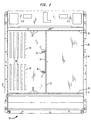
- FIG. 1 shows a card cage, designated generally by the reference numeral 10, with which the present invention finds utility.
- the card cage 10 is typically mounted to an equipment rack, by means of the flanges 12, and includes an exterior metal enclosure 14.
- the card cage 10 includes parallel spaced apart upper plate 16 and lower plate 18 secured to the enclosure 14.
- the upper and lower plates 16, 18 are substantially the same and provide a plurality of parallel guide slots 20 for a plurality of circuit packs.
- the plates 16, 18 are stamped and formed to have cutouts with upturned edges to provide the guide slots 20 between adjacent upturned edges.
- a separator plate 22 may be provided to which is secured a member 24 having opposed flanges 25, 26 on which are formed guide slots 27 so that smaller circuit packs may be accommodated in the card cage 10.
- a backplane 28 mounted to the back of the enclosure 14 is a backplane 28, as shown in Figure 2.
- the backplane 28 is a planar circuit board having an array of connectors 30 secured thereto.
- the connectors 30 are so situated on the backplane 28 that when a circuit pack is inserted into a pair of opposed guide slots 20, the connector on the circuit pack engages respective connector(s) 30 upon being fully inserted into the enclosure 14.
- the problem which the present invention solves arises due to the close spacing between adjacent guide slots 20. If a circuit pack is not initially inserted at the correct angle into a pair of guide slots, metal shielding on a circuit pack connector can inadvertently contact circuitry on an adjacent circuit pack.
- FIG. 3 illustrates a circuit pack, designated generally by the reference numeral 32, in which is incorporated the present invention.
- the circuit pack 32 includes a circuit board 34 having a pair of opposed parallel side edges 36, 38, and a forward edge 40 extending between the side edges 36, 38.
- Connector arrays 42 are secured to the circuit board 34 and extend forwardly beyond the forward edge 40 of the board 34.
- the connector arrays 42 have a forward mating end 44 adapted to engage respective connectors 30 on the backplane 28.
- Circuit components 46 are mounted to the circuit board 34 and circuitry 48 on the board 34 connects the circuit components 46 to the connector array 42.
- the circuit board 34 is formed to have a pair of tabs 50, 52 which extend forwardly beyond the mating end 44 of the connector arrays 42.
- Each of the tabs 50, 52 has an edge which is an extension of a respective one of the side edges 36, 38.
- the forward edge 40 of the circuit card 34 is recessed over a portion of its length to form the tabs 50, 52.
- the tabs 50, 52 extend forwardly to a line 54 which is orthogonal to the side edges 36, 38, and the mating end 44 of the connector arrays 42 is between the line 54 and the forward edge 40 of the circuit card 34.
- the tab 52 enters the guide slot in advance of the mating end 44 of the connector arrays 42.
- the circuit board 34 is properly aligned before the shielding 56 on the connector arrays 42 is inserted far enough to short an adjacent circuit pack.
- the broken line 40' is an extension of the forward edge 40 of the circuit card 34 and it is seen that without the tab 52 if the circuit card 34 was not properly in the guide slot until the forward edge 40 reached the beginning of the guide slot, the shielding 56 could be offset sufficiently to short an adjacent circuit pack.
- the tabs 50, 52 provide a degree of protection to the connector arrays 42 against inadvertent mishandling.
Landscapes
- Engineering & Computer Science (AREA)
- Microelectronics & Electronic Packaging (AREA)
- Details Of Connecting Devices For Male And Female Coupling (AREA)
- Mounting Of Printed Circuit Boards And The Like (AREA)
- Coupling Device And Connection With Printed Circuit (AREA)
- Casings For Electric Apparatus (AREA)
Applications Claiming Priority (2)
| Application Number | Priority Date | Filing Date | Title |
|---|---|---|---|
| US26814999A | 1999-03-15 | 1999-03-15 | |
| US268149 | 1999-03-15 |
Publications (2)
| Publication Number | Publication Date |
|---|---|
| EP1037516A2 true EP1037516A2 (de) | 2000-09-20 |
| EP1037516A3 EP1037516A3 (de) | 2001-04-11 |
Family
ID=23021700
Family Applications (1)
| Application Number | Title | Priority Date | Filing Date |
|---|---|---|---|
| EP00301873A Withdrawn EP1037516A3 (de) | 1999-03-15 | 2000-03-07 | Fortgeschrittene Führung in Nut für eine Leiterplattenbaugruppe und Verbinderschutz |
Country Status (5)
| Country | Link |
|---|---|
| EP (1) | EP1037516A3 (de) |
| JP (1) | JP2000277929A (de) |
| CN (1) | CN1267183A (de) |
| AU (1) | AU2077800A (de) |
| CA (1) | CA2299714A1 (de) |
Family Cites Families (2)
| Publication number | Priority date | Publication date | Assignee | Title |
|---|---|---|---|---|
| US5317480A (en) * | 1992-08-21 | 1994-05-31 | At&T Bell Laboratories | Circuit pack interconnection |
| JPH0846377A (ja) * | 1994-08-04 | 1996-02-16 | Fujitsu Ltd | プリント配線板パッケージ収容用シェルフ |
-
2000
- 2000-02-29 CA CA 2299714 patent/CA2299714A1/en not_active Abandoned
- 2000-03-07 EP EP00301873A patent/EP1037516A3/de not_active Withdrawn
- 2000-03-09 AU AU20778/00A patent/AU2077800A/en not_active Abandoned
- 2000-03-13 JP JP2000069356A patent/JP2000277929A/ja active Pending
- 2000-03-14 CN CN 00104123 patent/CN1267183A/zh active Pending
Also Published As
| Publication number | Publication date |
|---|---|
| EP1037516A3 (de) | 2001-04-11 |
| CN1267183A (zh) | 2000-09-20 |
| JP2000277929A (ja) | 2000-10-06 |
| AU2077800A (en) | 2000-09-21 |
| CA2299714A1 (en) | 2000-09-15 |
Similar Documents
| Publication | Publication Date | Title |
|---|---|---|
| US5961350A (en) | Modular side-by-side connectors | |
| US7686622B2 (en) | Plug connector with mating protection | |
| US7748997B2 (en) | Receptacle for electrical connectors | |
| US5221212A (en) | Shielding a surface mount electrical connector | |
| US7278856B2 (en) | Contact protector for electrical connectors | |
| US7303438B2 (en) | Plug connector with mating protection and alignment means | |
| US5688130A (en) | Electrical connector assembly for pc cards | |
| USRE43427E1 (en) | Plug connector with mating protection | |
| US5755592A (en) | Combined ground strap and board lock for electrical connector assembly | |
| US6120318A (en) | Stacked electrical connector having visual indicator subassembly | |
| EP0337634A1 (de) | Bezugsleitung zur Verbesserung der Integrität der Signale in elektrischen Steckverbindern | |
| EP0730324A2 (de) | Verbesserter abgeschirmter kompakter Datensteckverbinder | |
| GB2223634A (en) | Grounding clip for electrostatic dissipation in electrical connectors | |
| US6932626B2 (en) | Electrical card connector | |
| CN110323632A (zh) | 电连接器的触头模块的屏蔽结构 | |
| EP0584937B1 (de) | Abschirmung eines oberflächenmontierten elektrischen Verbinders | |
| EP0836147A2 (de) | System zur Erdung einer Chipkarte | |
| JP2020510294A (ja) | 通信システム用の回路カードアセンブリ | |
| US20040023537A1 (en) | ESD type connector | |
| US5317480A (en) | Circuit pack interconnection | |
| US6280257B1 (en) | Cable dock fixture with EMI shielding | |
| US6444900B1 (en) | Electromagnetic interference shielding gasket | |
| US6109969A (en) | Cable connector having improved EMI shields for securely grounding to a panel of a mating connector | |
| EP0774807A2 (de) | Elektrischer Verbinder | |
| CA2299714A1 (en) | Circuit pack advanced guidance into guide slot and connector protection |
Legal Events
| Date | Code | Title | Description |
|---|---|---|---|
| PUAI | Public reference made under article 153(3) epc to a published international application that has entered the european phase |
Free format text: ORIGINAL CODE: 0009012 |
|
| AK | Designated contracting states |
Kind code of ref document: A2 Designated state(s): AT BE CH CY DE DK ES FI FR GB GR IE IT LI LU MC NL PT SE |
|
| AX | Request for extension of the european patent |
Free format text: AL;LT;LV;MK;RO;SI |
|
| PUAL | Search report despatched |
Free format text: ORIGINAL CODE: 0009013 |
|
| AK | Designated contracting states |
Kind code of ref document: A3 Designated state(s): AT BE CH CY DE DK ES FI FR GB GR IE IT LI LU MC NL PT SE |
|
| AX | Request for extension of the european patent |
Free format text: AL;LT;LV;MK;RO;SI |
|
| RIC1 | Information provided on ipc code assigned before grant |
Free format text: 7H 05K 7/14 A, 7H 01R 13/631 B |
|
| AKX | Designation fees paid | ||
| REG | Reference to a national code |
Ref country code: DE Ref legal event code: 8566 |
|
| STAA | Information on the status of an ep patent application or granted ep patent |
Free format text: STATUS: THE APPLICATION IS DEEMED TO BE WITHDRAWN |
|
| 18D | Application deemed to be withdrawn |
Effective date: 20011012 |