EP1037342A2 - Semiconductor laser device and fabrication method thereof - Google Patents
Semiconductor laser device and fabrication method thereof Download PDFInfo
- Publication number
- EP1037342A2 EP1037342A2 EP00104472A EP00104472A EP1037342A2 EP 1037342 A2 EP1037342 A2 EP 1037342A2 EP 00104472 A EP00104472 A EP 00104472A EP 00104472 A EP00104472 A EP 00104472A EP 1037342 A2 EP1037342 A2 EP 1037342A2
- Authority
- EP
- European Patent Office
- Prior art keywords
- laser device
- semiconductor laser
- inp
- active regions
- layer
- Prior art date
- Legal status (The legal status is an assumption and is not a legal conclusion. Google has not performed a legal analysis and makes no representation as to the accuracy of the status listed.)
- Withdrawn
Links
Images





Classifications
-
- H—ELECTRICITY
- H01—ELECTRIC ELEMENTS
- H01S—DEVICES USING THE PROCESS OF LIGHT AMPLIFICATION BY STIMULATED EMISSION OF RADIATION [LASER] TO AMPLIFY OR GENERATE LIGHT; DEVICES USING STIMULATED EMISSION OF ELECTROMAGNETIC RADIATION IN WAVE RANGES OTHER THAN OPTICAL
- H01S5/00—Semiconductor lasers
- H01S5/10—Construction or shape of the optical resonator, e.g. extended or external cavity, coupled cavities, bent-guide, varying width, thickness or composition of the active region
- H01S5/12—Construction or shape of the optical resonator, e.g. extended or external cavity, coupled cavities, bent-guide, varying width, thickness or composition of the active region the resonator having a periodic structure, e.g. in distributed feedback [DFB] lasers
- H01S5/1228—DFB lasers with a complex coupled grating, e.g. gain or loss coupling
-
- B—PERFORMING OPERATIONS; TRANSPORTING
- B82—NANOTECHNOLOGY
- B82Y—SPECIFIC USES OR APPLICATIONS OF NANOSTRUCTURES; MEASUREMENT OR ANALYSIS OF NANOSTRUCTURES; MANUFACTURE OR TREATMENT OF NANOSTRUCTURES
- B82Y20/00—Nanooptics, e.g. quantum optics or photonic crystals
-
- H—ELECTRICITY
- H01—ELECTRIC ELEMENTS
- H01S—DEVICES USING THE PROCESS OF LIGHT AMPLIFICATION BY STIMULATED EMISSION OF RADIATION [LASER] TO AMPLIFY OR GENERATE LIGHT; DEVICES USING STIMULATED EMISSION OF ELECTROMAGNETIC RADIATION IN WAVE RANGES OTHER THAN OPTICAL
- H01S5/00—Semiconductor lasers
- H01S5/10—Construction or shape of the optical resonator, e.g. extended or external cavity, coupled cavities, bent-guide, varying width, thickness or composition of the active region
- H01S5/12—Construction or shape of the optical resonator, e.g. extended or external cavity, coupled cavities, bent-guide, varying width, thickness or composition of the active region the resonator having a periodic structure, e.g. in distributed feedback [DFB] lasers
- H01S5/1231—Grating growth or overgrowth details
-
- H—ELECTRICITY
- H01—ELECTRIC ELEMENTS
- H01S—DEVICES USING THE PROCESS OF LIGHT AMPLIFICATION BY STIMULATED EMISSION OF RADIATION [LASER] TO AMPLIFY OR GENERATE LIGHT; DEVICES USING STIMULATED EMISSION OF ELECTROMAGNETIC RADIATION IN WAVE RANGES OTHER THAN OPTICAL
- H01S5/00—Semiconductor lasers
- H01S5/20—Structure or shape of the semiconductor body to guide the optical wave ; Confining structures perpendicular to the optical axis, e.g. index or gain guiding, stripe geometry, broad area lasers, gain tailoring, transverse or lateral reflectors, special cladding structures, MQW barrier reflection layers
-
- H—ELECTRICITY
- H01—ELECTRIC ELEMENTS
- H01S—DEVICES USING THE PROCESS OF LIGHT AMPLIFICATION BY STIMULATED EMISSION OF RADIATION [LASER] TO AMPLIFY OR GENERATE LIGHT; DEVICES USING STIMULATED EMISSION OF ELECTROMAGNETIC RADIATION IN WAVE RANGES OTHER THAN OPTICAL
- H01S5/00—Semiconductor lasers
- H01S5/30—Structure or shape of the active region; Materials used for the active region
- H01S5/34—Structure or shape of the active region; Materials used for the active region comprising quantum well or superlattice structures, e.g. single quantum well [SQW] lasers, multiple quantum well [MQW] lasers or graded index separate confinement heterostructure [GRINSCH] lasers
- H01S5/341—Structures having reduced dimensionality, e.g. quantum wires
-
- H—ELECTRICITY
- H01—ELECTRIC ELEMENTS
- H01S—DEVICES USING THE PROCESS OF LIGHT AMPLIFICATION BY STIMULATED EMISSION OF RADIATION [LASER] TO AMPLIFY OR GENERATE LIGHT; DEVICES USING STIMULATED EMISSION OF ELECTROMAGNETIC RADIATION IN WAVE RANGES OTHER THAN OPTICAL
- H01S5/00—Semiconductor lasers
- H01S5/30—Structure or shape of the active region; Materials used for the active region
- H01S5/34—Structure or shape of the active region; Materials used for the active region comprising quantum well or superlattice structures, e.g. single quantum well [SQW] lasers, multiple quantum well [MQW] lasers or graded index separate confinement heterostructure [GRINSCH] lasers
- H01S5/343—Structure or shape of the active region; Materials used for the active region comprising quantum well or superlattice structures, e.g. single quantum well [SQW] lasers, multiple quantum well [MQW] lasers or graded index separate confinement heterostructure [GRINSCH] lasers in AIIIBV compounds, e.g. AlGaAs-laser, InP-based laser
- H01S5/34306—Structure or shape of the active region; Materials used for the active region comprising quantum well or superlattice structures, e.g. single quantum well [SQW] lasers, multiple quantum well [MQW] lasers or graded index separate confinement heterostructure [GRINSCH] lasers in AIIIBV compounds, e.g. AlGaAs-laser, InP-based laser emitting light at a wavelength longer than 1000nm, e.g. InP based 1300 and 1500nm lasers
-
- H—ELECTRICITY
- H01—ELECTRIC ELEMENTS
- H01S—DEVICES USING THE PROCESS OF LIGHT AMPLIFICATION BY STIMULATED EMISSION OF RADIATION [LASER] TO AMPLIFY OR GENERATE LIGHT; DEVICES USING STIMULATED EMISSION OF ELECTROMAGNETIC RADIATION IN WAVE RANGES OTHER THAN OPTICAL
- H01S5/00—Semiconductor lasers
- H01S5/30—Structure or shape of the active region; Materials used for the active region
- H01S5/34—Structure or shape of the active region; Materials used for the active region comprising quantum well or superlattice structures, e.g. single quantum well [SQW] lasers, multiple quantum well [MQW] lasers or graded index separate confinement heterostructure [GRINSCH] lasers
- H01S5/343—Structure or shape of the active region; Materials used for the active region comprising quantum well or superlattice structures, e.g. single quantum well [SQW] lasers, multiple quantum well [MQW] lasers or graded index separate confinement heterostructure [GRINSCH] lasers in AIIIBV compounds, e.g. AlGaAs-laser, InP-based laser
- H01S5/3434—Structure or shape of the active region; Materials used for the active region comprising quantum well or superlattice structures, e.g. single quantum well [SQW] lasers, multiple quantum well [MQW] lasers or graded index separate confinement heterostructure [GRINSCH] lasers in AIIIBV compounds, e.g. AlGaAs-laser, InP-based laser with a well layer comprising at least both As and P as V-compounds
Definitions
- the present invention relates to a semiconductor laser device suitable for use as a light source which is used for long distance, large optical communication.
- the present invention father relates to a method for fabricating such a semiconductor laser device.
- the quantum wire structure has a high gain property relative to a quantum thin film structure.
- the semiconductor laser having the quantum wire structure operates with a small current, with high efficiency, and with narrow spectral linewidth (M. Asada et al., IEEE JQE, vol. QE-22, No.9, pp.1915-1921, 1986).
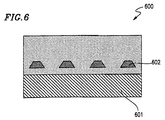
- Figure 6 shows a conventional semiconductor laser device 600 having a quantum wire structure (Arai et al., Proceedings of Electronics Society Conference of Institute of Electronics, Information and Communication Engineers. 1997, pp. 266-267).
- double-quantum well active regions 602 each having a trapezoid shape are formed above an InP substrate 601 , and the width of the trapezoid is about 35 nm in the center portion thereof.
- the well regions 602 each have a thickness of 10 nm, and form a quantum wire structure.
- a method for fabricating the conventional semiconductor laser device 600 having a quantum wire structure is described with reference to parts (a) to (c) of Figure 7 .
- an InGaAsP light confinement layer 603 in the first crystal growth process, an InGaAsP light confinement layer 603 .
- a quantum well active layer 604 having two wells, and an InGaAsP protective layer 605 are serially formed on a p-type InP substrate 601 .
- predetermined portions of the quantum well active layer 604 are selectively etched, thereby forming a plurality of double-quantum well active regions 602 each having a trapezoid shape in a periodic pattern.
- an undoped InP layer 606 , InGaAsP light confinement layer 607 , and an n-type InP cladding layer 608 are grown through a crystal growth process, thereby confining the double-quantum well active regions 602 each having a trapezoid shape.
- the quantum well active layer 604 it is necessary to once etch the quantum well active layer 604 so that the quantum well active layer 604 has a quantum wire structure, and faces exposed by etching are exposed to a thermal treatment during a subsequent regrowth process.
- a thermal treatment may introduce a defect by etching a portion of the quantum well active regions 602 , and the defect may deteriorate an optical property of the quantum well active regions 602 .
- the long-term reliability of the semiconductor laser device may decrease.
- the size of the quantum wire structure having a trapezoid shape, which is formed by etching varies according to even a small variation of the concentration of an etching solution. Thus, it is difficult to fabricate a quantum wire structure having a uniform size.
- a semiconductor laser device include. an InP substrate and a multi-layered structure farmed on the InP substrate, wherein the multi-layered structure includes at least a plurality of active regions for outputting a laser beam, and the plurality of active regions each are provided in each of a plurality of grooves dented toward the InP substrate.
- the cross-sectional shape of each of the plurality of grooves is a triangle dented toward the InP substrate.
- the plurality of active regions is made of InAsP.
- the active regions are formed in a periodic pattern in a direction parallel to the resonator length direction.
- the semiconductor laser device further includes: an InP layer; and a light confinement layer made of a semiconductor having a bandgap energy between the bandgap energy of a semiconductor constituting the active regions and the bandgap energy of InP, wherein the active regions are provided between the light confinement layer and the InP layer.
- the semiconductor laser device further include. a light confinement layer made of a semiconductor having a bandgap energy between the bandgap energy of a semiconductor constituting the active regions and the bandgap energy of InP, wherein the active regions are surrounded by the light confinement layer.
- the light confinement layer is made of InGaAsP.
- the active regions each has a multiquantum well structure.
- a well layer of the multiquantum well structure is made of InAsP.
- a barrier layer of the multiquantum well structure is made of InP.
- the active regions each has a size such that a quantum size effect is obtained.
- the pitch of the active regions is a multiple of (l/(2 ⁇ neff)) by a factor of any integer, where neff is the effective refractive index of the multi-layered structure with respect to an oscillation wavelength.
- a method for fabricating a semiconductor laser device includes steps of: forming a plurality of grooves in a surface of an InP layer: and thermally treating the InP layer in an atmosphere including at least a gas containing phosphorus and a gas containing arsenic in a mixed state, thereby forming a plurality of active regions made of InAsP in the plurality of grooves.
- each of the grooves is formed in a triangle shape such that a bottom of the triangle is on a surface of the InP layer.
- the InP layer is an uppermost layer of a multi-layered structure.
- the method for fabricating a semiconductor laser device further includes a step of forming a light confinement layer adjacent to the InP layer, wherein the light confinement layer made of a semiconductor having a bandgap energy between the bandgap energy of a semiconductor constituting the active regions between the InP substrate and the InP layer and the bandgap energy of InP.
- the step of thermally treating the InP layer includes a step of intermittently providing a gas containing arsenic, thereby forming a plurality of active regions each having a well layer made of InAsP in the plurality of grooves.
- the semiconductor laser device includes a step of forming a light confinement layer adjacent to the InP layer, wherein the light confinement layer made of a semiconductor having a bandgap energy between the bandgap energy of a semiconductor constituting the active regions between the InP substrate and the InP layer and the bandgap energy of InP.
- the light confinement layer is made of InGaAsP.
- the plurality of grooves have a periodic pattern in a direction parallel to a resonator length direction.
- the invention described herein makes possible the advantages of (1) providing a semiconductor laser device having a quick response property and a long-term reliability, and a fabrication method of such a semiconductor laser device: (2) providing a semiconductor laser device having active regions as small as several tens of nanometers which are arranged at a high density, and thus functioning as a quantumwire laser; and (3) providing a distributed feedback type semiconductor laser including periodically formed active regions that function as a diffraction grating, and thus being capable of oscillating with a single wavelength, providing a low noise property, enabling a long distance optical transmission, etc.
- Figure 1A is a crags-sectional view of a semiconductor laser device 100 according to one embodiment of the present invention showing a facet perpendicular to a resonator length direction.
- Figure 1B is a cross-sectional view showing a facet of the semiconductor laser device 100 parallel to the resonator length direction.
- Figure 1A is a cross-sectional view of the semiconductor laser device 100 taken along line A-A' of Figure 1B .
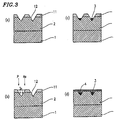
- Parts (a) to (e) of Figure 2 and parts (a) to (d) of Figure 3 are cross-sectional views showing a fabrication method of the semiconductor laser device 100 according to the present invention.
- Parts (a) to (e) of Figure 2 and parts (a) to (d) of Figure 3 each show a facet of the semiconductor laser device 100 parallel to the resonator length direction.
- Figure 4 is a graph showing a characteristic of the semiconductor laser device 100 according to the present invention.
- the semiconductor laser device 100 has a broad area structure having a stripe width of 100 ⁇ m.
- the resonator length is 750 ⁇ m.
- An n-side electrode 7 made of Ti/Au is formed on the back surface of the n-type InP substrate 1 .
- An SiO 2 insulating film 9 including a stripe-shaped window 8 (width: 100 ⁇ m) is formed on the p-type InGaAs contact layer 6 .
- a p-side electrode made of Ti/Au is formed on the SiO 2 insulating film 9 so as to be in contact with the p-type InGaAs contact layer 6 through the stripe-shaped window 8 .
- the plurality of InAsP active regions 3 are formed at a pitch of 238 nm in the resonator length direction between the undoped InGaAsP light confinement layer 2 and the undoped InP buffer layer 4 .
- the shape of the InAsP active regions 3 seen on a facet parallel to the resonator length direction and perpendicular to the top face of the n-type InP substrate 1 , is triangular. Each side of the triangle is about 25 nm, and one apex extends toward the n-type InP substrate 1 .
- the active region 3 will be described later with reference to Figure 2 .
- the semiconductor laser device 100 according to the present invention it is possible to uniformly form small active regions having a size of about several tens of nanometers because it is not necessary to etch the active regions. With such small active regions, the sought effects of quantum wire can be realized.
- the photoluminescence wavelength of the InAsP active regions 3 formed periodically in the resonator length direction is set to about 1.55 ⁇ m.
- the Bragg wavelength that is determined by the pitch of the InAsP active regions 3 is 1.53 ⁇ m, obtaining a laser oscillation having a single wavelength at the Bragg wavelength.
- the undoped InGaAsP light confinement layer 2 and the pitch of the InAsP active regions 3 are alternately provided in a resonator length direction in an interface area therebetween.
- the refractive index difference is small relative to that in a structure in which the undoped InP buffer layer 4 and the InAsP active region 3 are provided alternately in the resonator length direction.
- the ratio of a gain coupling becomes larger than that of a refractive index coupling, thereby increasing the probability of the oscillation with a single wavelength.
- FIG. 1A and 1B A fabrication method of the semiconductor laser device 100 shown in Figures 1A and 1B is described with reference to Figure 2 .
- the undoped InGaAsP light confinement layer 2 (thickness: 150 nm) and an InP provisional layer 11 are formed on the n-type InP substrate 1 by the metal organic vapor phase growing method.
- a diffraction grating 12 (pitch 238 nm, depth 200 nm) in the form of grooves dented toward the InP substrate 1 , having a stripe-shape in a ⁇ 1-10 ⁇ direction, is formed by etching and by a two luminous flux interference exposure method so that the etched groove is formed in the undoped InGaAsP light confinement layer 2 .
- tert-butyl phosphine and tert-butyl arsine are introduced into a hydrogen atmosphere, and the n-type InP substrate 1 is heated to 550°C in the resultant atmosphere.
- the InAsP active regions 3 are formed in concave portions of the diffraction grating 12 so as to have a thickness of about 10 nm as shown in part (c) of Figure 2 .
- the provision of tert-butyl arsine is stopped while the thermal treatment continues, whereby an undoped InP buffer layer 4 (thickness:150 nm) is formed on the InAsP active regions 3 so that the undoped InP buffer layer 4 has a flat top surface.
- an SiO 2 insulating film is formed on the p-type InGaAs contact layer 6 , and a stripe-shaped window (width: 100 ⁇ m) is formed in the SiO 2 insulating film. Then, a p-side electrode 10 made of Ti/Au is formed on the SiO 2 insulating film. Furthermore, a n-side electrode 7 made of Ti/Au is formed on the back face of the n-type InP substrate 1 . After the cleavage process, a semiconductor laser device 100 is completed.
- the active regions 3 are not etched. Thus, atoms rarely leak out from the surface of the active regions 3 even when the temperature becomes high during the time when the semiconductor film is grown after the etching.
- Part (a) of Figure 3 is a cross-sectional view of a structure including an n-type InP substrate 1 , an undoped InGaAsP light confinement layer 2 and an InP provisional layer 11 .
- a diffraction grating 12 is formed by etching as shown in part (a) of Figure 3 .
- the resultant structure shown in part (a) of Figure 3 is thermally treated in an atmosphere containing tert-butyl phosphine and tert-butyl arsine in a mixed state.
- the InAsP regions 3 are periodically provided, and each of them is formed in an inverted triangle shape.
- the supply of tert-butyl arsine is stopped while the thermal treatment continues, thereby forming an undoped InP buffer layer 4 of In mass-transported from the remaining InP provisional layer 11 and P from degraded tert-butyl.
- phosphine on the InAsP regions 3 and the undoped InGaAsP light confinement layer 2 so as to have a flat top surface.
- the flat surface of the undoped InP buffer layer 4 is significant for preventing the degradation of the crystal quality of layers to be formed on the undoped InP buffer layer 4 .
- the thickness of the InAsP regions 3 be 50 nm or less.
- tert-butyl phosphine and tert-butyl arsine are used as a gas containing phosphorus and a gas containing arsenic, respectively. Therefore, it is possible to maintain the degradation efficiency of each of the gases in a temperature range in which the mass-transport occurs during the increase of the temperature. Accordingly, it is possible to obtain the uniform composition in the InAsP active regions 3 along a direction of the thickness thereof.
- FIG 4 shows the oscillation spectrum of the semiconductor laser device 100 shown in Figure 1 .
- the measurement was carried out by supplying a pulse current having a cycle of 1 ⁇ s and a duty of 0.01% to the semiconductor laser device 100 at a room temperature.
- An oscillation in the vicinity of a Bragg wavelength of 1.53 ⁇ m was observed, even though the oscillation was a transverse multimode oscillation because the stripe width of the semiconductor laser device 100 is as large as 100 ⁇ m.
- a threshold current density was 0.16 kA/cm 2 . It is reported that in the conventional semiconductor laser device 600 shown in Figure 6 , a threshold current density was 2.4 kA/cm 2 . That is, according to the semiconductor laser device 100 of the present invention, the threshold current is significantly reduced.
- the present embodiment employs a broad area structure.
- a buried hetero structure it is possible to realize a lower threshold current characteristic.
- tert-butyl phosphine is used as a gas containing phosphorus.
- phosphine tert-butyl arsine is used as a gas containing arsenic.
- arsine is used as a gas containing arsenic.
- Figure 5A is a cross-sectional view of a semiconductor laser device 500 according to another embodiment of the present invention showing a facet thereof perpendicular to a resonator length direction.
- Figure 5B is a cross-sectional view of the semiconductor laser device 500 showing a facet thereof parallel to the resonator length direction.
- Figure 5A is a cross-sectional view of the semiconductor laser device 500 taken along line A-A' of Figure 5B .
- Figure 5C is an enlarged view of active regions 501 .
- the semiconductor laser device 500 has the same structure as that of the semiconductor laser device 100 shown in Figures 1A and 1B except for the active regions 501 .
- the active regions 501 of the semiconductor laser device 500 each have a multiquantum well structure including barrier layers 502 and well layers 503 deposited alternately in concave portions of the light confinement layer 2 .
- the barrier layers 502 are made of InP
- the well layers 503 are made of InAsP.
- each of the well layers 503 has a thickness of 10 nm or less so that a quantum size effect is obtained.
- a fabrication method of the semiconductor laser device 500 is substantially the same as that of the semiconductor laser device 100 which has been described with reference to Figures 2 and 3 . However, between these methods, there is a difference in that the active regions 501 of the semiconductor laser device 500 are formed so that the active regions 501 each include the barrier layers 502 and the well layers 503 .
- a well layer 503 is formed of InAsP in a groove by the same method as used for forming the active regions 3 of the semiconductor laser device 100 , a barrier layer 502 is formed of InP on the resultant well layer 503 by the same method as used for forming the buffer layer 4 of the semiconductor laser device 100 , i.e., by stopping the provision of tert-butyl arsine halfway in the thermal treatment, and these steps may be alternately repeated, thereby forming the multiquantum well structure of the active regions 501 .
- a band gap energy of the light confinement layer is between a band gap energy of InP and a band gap energy of the active regions.
- a desirable band gap energy is described in Japanese Laid-Open Publication No. 3-25990.
- the undoped InGaAsP light confinement layer 2 and the undoped InP buffer layer 4 may be made of the same material, and the active regions 3 may be sandwiched by the light confinement layer 2 and the buffer layer 4 (i.e., another light confinement layer).
- each active region is formed in the groove in a triangle shape.
- the shape of the grooves i.e., the shape of active regions formed in the grooves
- the shape of the grooves is not limited to a triangle as long as grooves are formed so as to have any shape, and the active regions are formed in these grooves.
- the active regions are formed in a periodic pattern (i.e., the grooves are formed in a periodic pattern in the light confinement layer 2 ).
- the pitch of the active regions is a multiple of (l/(2 ⁇ neff)) by a factor of any integer, where neff is the effective refractive index of the multi-layered structure with respect to an oscillation wavelength.
- a semiconductor laser of the present invention since the size of semiconductor regions formed in grooves is uniform, an effect of a quantum wire can be easily obtained.
- a semiconductor laser device of the present invention is a gain coupled, distributed feedback type semiconductor laser device, the semiconductor laser device produces a quantum wire effect, and there is a high probability that the oscillation occurs with a single wavelength in such a semiconductor laser device. Furthermore, even in the presence of return light from outside of the laser device, the mode of the laser does not change, and the laser device is not susceptible to noise.
- active regions are periodically formed without the active regions being subjected to an etching step. Therefore, after the active regions are formed, it is possible to grow semiconductor layers of fine quality.
- a semiconductor laser device fabricated according to such a fabrication method exhibits high reliability for a long term. Furthermore, since the active regions are formed not by etching but by a vapor phase growing method, the active regions can be formed with considerable control accuracy.
- the fabrication process is simple and easy, and is a process of great versatility.
- a semiconductor laser device of the present invention is a distributed feedback type semiconductor laser device
- the semiconductor laser device produces a quantum wire effect
- a light source can be fabricated with relatively loose restrictions in design of a spectral linewidth at a high production yield.
- a light source can be fabricated with relatively loose restrictions in design of a spectral linewidth through a considerably simple process with great applicability.
- a semiconductor laser device fabricated according to the present invention has a great practical value.
Landscapes
- Physics & Mathematics (AREA)
- Optics & Photonics (AREA)
- Chemical & Material Sciences (AREA)
- Engineering & Computer Science (AREA)
- Nanotechnology (AREA)
- Condensed Matter Physics & Semiconductors (AREA)
- General Physics & Mathematics (AREA)
- Electromagnetism (AREA)
- Life Sciences & Earth Sciences (AREA)
- Biophysics (AREA)
- Crystallography & Structural Chemistry (AREA)
- Semiconductor Lasers (AREA)
Abstract
Description
Claims (20)
- A semiconductor laser device comprising an InP substrate and a multi-layered structure formed on the InP substrate, whereinthe multi-layered structure includes at least a plurality of active regions for outputting a laser beam, andthe plurality of active regions each are provided in each of a plurality of grooves dented toward the InP substrate.
- A semiconductor laser device according to claim 1, wherein the cross-sectional shape of each of the plurality of grooves is a triangle dented toward the InP substrate.
- A semiconductor laser device according to claim 1 or 2, wherein the plurality of active regions is made of InAsP.
- A semiconductor laser device according to any of claims 1 to 3, wherein the active regions are formed in a periodic pattern in a direction parallel to the resonator length direction.
- A semiconductor laser device according to any of claims 1 to 4, further comprising:an InP layer; anda light confinement layer made of a semiconductor having a bandgap energy between the bandgap energy of a semiconductor constituting the active regions and the bandgap energy of InP,
wherein the active regions are provided between the light confinement layer and the InP layer. - A semiconductor laser device according to any of claims 1 to 4, further comprising a light confinement layer made of a semiconductor having a bandgap energy between the bandgap energy of a semiconductor constituting the active regions and the bandgap energy of InP,
wherein the active regions are surrounded by the light confinement layer. - A semiconductor laser device according to claim 5 or 6, wherein the light confinement layer is made of InGaAsP.
- A semiconductor laser device according to any of claims 1 to 7, wherein the active regions each has a multiquantum well structure.
- A semiconductor laser device according to claim 8, wherein a well layer of the multiquantum well structure is made of InAsP.
- A semiconductor laser device according to claim 8, wherein a barrier layer of the multiquantum well structure is made of InP.
- A semiconductor laser device according to any of claims 1 to 7, wherein the active regions each has a size such that a quantum size effect is obtained.
- A semiconductor laser device according to any of claims 1 to 11, wherein the pitch of the active regions is a multiple of (l/(2×neff)) by a factor of any integer, where neff is the effective refractive index of the multi-layered structure with respect to an oscillation wavelength.
- A method for fabricating a semiconductor laser device comprising steps of:forming a plurality of grooves in a surface of an InP layer;thermally treating the InP layer in an atmosphere including at least a gas containing phosphorus and a gas containing arsenic in a mixed state, thereby forming a plurality of active regions made of InAsP in the plurality of grooves.
- A method for fabricating a semiconductor laser device according to claim 13, wherein each of the grooves is formed in a triangle shape such that a bottom of the triangle is on a surface of the InP layer.
- A method for fabricating a semiconductor laser device according to claim 13, wherein the InP layer is an uppermost layer of a multi-layered structure.
- A method for fabricating a semiconductor laser device according to claim 15, further comprising a step of forming a light confinement layer adjacent to the InP layer, wherein the light confinement layer made of a semiconductor having a bandgap energy between the bandgap energy of a semiconductor constituting the active regions between the InP substrate and the InP layer and the bandgap energy of InP.
- A method for fabricating a semiconductor laser device according to claim 13 or 15, wherein the step of thermally treating the InP layer includes a step of intermittently providing a gas containing arsenic, thereby forming a plurality of active regions each having a well layer made of InAsP in the plurality of grooves.
- A method for fabricating a semiconductor laser device according to claim 17, comprising a step of forming a light confinement layer adjacent to the InP layer, wherein the light confinement layer made of a semiconductor having a bandgap energy between the bandgap energy of a semiconductor constituting the active regions between the InP substrate and the InP layer and the bandgap energy of InP.
- A method for fabricating a semiconductor laser device according to claim 16 or 18, wherein the light confinement layer is made of InGaAsP.
- A method for fabricating a semiconductor laser device according to any of claims 13 to 19, wherein the plurality of grooves have a periodic pattern in a direction parallel to a resonator length direction.
Applications Claiming Priority (2)
| Application Number | Priority Date | Filing Date | Title |
|---|---|---|---|
| JP11059790A JP2000261104A (en) | 1999-03-08 | 1999-03-08 | Semiconductor laser device and method of manufacturing the same |
| JP5979099 | 1999-03-08 |
Publications (2)
| Publication Number | Publication Date |
|---|---|
| EP1037342A2 true EP1037342A2 (en) | 2000-09-20 |
| EP1037342A3 EP1037342A3 (en) | 2001-12-05 |
Family
ID=13123442
Family Applications (1)
| Application Number | Title | Priority Date | Filing Date |
|---|---|---|---|
| EP00104472A Withdrawn EP1037342A3 (en) | 1999-03-08 | 2000-03-08 | Semiconductor laser device and fabrication method thereof |
Country Status (3)
| Country | Link |
|---|---|
| US (2) | US6625189B1 (en) |
| EP (1) | EP1037342A3 (en) |
| JP (1) | JP2000261104A (en) |
Cited By (1)
| Publication number | Priority date | Publication date | Assignee | Title |
|---|---|---|---|---|
| CN103545711A (en) * | 2013-10-22 | 2014-01-29 | 中国科学院半导体研究所 | Distributed feedback laser and its preparation method |
Families Citing this family (5)
| Publication number | Priority date | Publication date | Assignee | Title |
|---|---|---|---|---|
| JP3681693B2 (en) * | 2002-02-21 | 2005-08-10 | Nec化合物デバイス株式会社 | Semiconductor laser and semiconductor optical integrated circuit including this element |
| US6724795B2 (en) * | 2002-05-10 | 2004-04-20 | Bookham Technology, Plc | Semiconductor laser |
| JP4325558B2 (en) * | 2005-01-05 | 2009-09-02 | 住友電気工業株式会社 | Semiconductor laser and method of manufacturing the semiconductor laser |
| JP5181787B2 (en) | 2008-04-01 | 2013-04-10 | 三菱電機株式会社 | Manufacturing method of semiconductor device |
| US10896601B2 (en) | 2016-09-21 | 2021-01-19 | Drive Safe Enforcement, Llc | Mobile traffic violation detection, recording and evidence processing system |
Family Cites Families (9)
| Publication number | Priority date | Publication date | Assignee | Title |
|---|---|---|---|---|
| US4673846A (en) | 1984-03-02 | 1987-06-16 | Mitsubishi Denki Kabushiki Kaisha | Microwave discharge light source apparatus |
| JPH01106489A (en) * | 1987-10-20 | 1989-04-24 | Fujitsu Ltd | Semiconductor device and manufacture thereof |
| JPH0325990A (en) * | 1989-06-23 | 1991-02-04 | Nec Corp | Optical semiconductor element |
| US5114877A (en) * | 1991-01-08 | 1992-05-19 | Xerox Corporation | Method of fabricating quantum wire semiconductor laser via photo induced evaporation enhancement during in situ epitaxial growth |
| US5138625A (en) * | 1991-01-08 | 1992-08-11 | Xerox Corporation | Quantum wire semiconductor laser |
| IT1245541B (en) * | 1991-05-13 | 1994-09-29 | Cselt Centro Studi Lab Telecom | SEMICONDUCTOR LASER WITH DISTRIBUTED REACTION AND PAIR OF GAIN, AND PROCEDURE FOR ITS MANUFACTURE |
| JP2763090B2 (en) | 1994-09-28 | 1998-06-11 | 松下電器産業株式会社 | Semiconductor laser device, manufacturing method thereof, and crystal growth method |
| EP0706243A3 (en) * | 1994-09-28 | 1996-11-13 | Matsushita Electric Industrial Co Ltd | Semiconductor laser with distributed reflector and method of making |
| JPH1022564A (en) * | 1996-07-02 | 1998-01-23 | Nec Corp | Semiconductor laser, and semiconductor light modulator, and manufacture of semiconductor laser |
-
1999
- 1999-03-08 JP JP11059790A patent/JP2000261104A/en active Pending
-
2000
- 2000-03-08 US US09/521,512 patent/US6625189B1/en not_active Expired - Fee Related
- 2000-03-08 EP EP00104472A patent/EP1037342A3/en not_active Withdrawn
-
2003
- 2003-07-28 US US10/628,550 patent/US6933159B2/en not_active Expired - Fee Related
Cited By (2)
| Publication number | Priority date | Publication date | Assignee | Title |
|---|---|---|---|---|
| CN103545711A (en) * | 2013-10-22 | 2014-01-29 | 中国科学院半导体研究所 | Distributed feedback laser and its preparation method |
| CN103545711B (en) * | 2013-10-22 | 2015-12-30 | 中国科学院半导体研究所 | Distributed feedback laser and preparation method thereof |
Also Published As
| Publication number | Publication date |
|---|---|
| JP2000261104A (en) | 2000-09-22 |
| US20040022290A1 (en) | 2004-02-05 |
| EP1037342A3 (en) | 2001-12-05 |
| US6933159B2 (en) | 2005-08-23 |
| US6625189B1 (en) | 2003-09-23 |
Similar Documents
| Publication | Publication Date | Title |
|---|---|---|
| US6426515B2 (en) | Semiconductor light-emitting device | |
| US6541297B2 (en) | Method for fabricating semiconductor device and semiconductor device | |
| US5684823A (en) | Method of fabricating a diffraction grating and a distributed feedback semiconductor laser incorporating the diffraction grating | |
| US20130267052A1 (en) | Semiconductor light emitting device and method for manufacturing the same | |
| US20040042516A1 (en) | DFB semiconductor laser device having ununiform arrangement of a diffraction grating | |
| JP2001244576A (en) | Optical semiconductor device and its manufacturing method | |
| KR100632308B1 (en) | Gain-coupled distributed feedback semiconductor laser device and manufacturing method thereof | |
| JP3204474B2 (en) | Gain-coupled distributed feedback semiconductor laser and its fabrication method | |
| US6625189B1 (en) | Semiconductor laser device and fabrication method thereof | |
| JPH11163464A (en) | Distribution feedback type semiconductor laser | |
| US20050123018A1 (en) | Ridge type distributed feedback semiconductor laser | |
| KR100278546B1 (en) | Semiconductor laser device | |
| KR100602973B1 (en) | Single-mode laser diode using strain-compensated multilayer quantum well and its manufacturing method | |
| US6867057B2 (en) | Method of manufacturing a semiconductor laser | |
| JP4999038B2 (en) | Manufacturing method of semiconductor device | |
| JP2763090B2 (en) | Semiconductor laser device, manufacturing method thereof, and crystal growth method | |
| JP2950297B2 (en) | Distributed feedback semiconductor laser and method of manufacturing the same | |
| JP3250270B2 (en) | Semiconductor laser device and method of manufacturing the same | |
| JP2903321B2 (en) | Method of manufacturing semiconductor laser device | |
| JP3189881B2 (en) | Semiconductor laser and method of manufacturing the same | |
| JPH06283802A (en) | Semiconductor laser device and fabrication thereof | |
| JPH09283850A (en) | Semiconductor distributed feedback laser device and manufacturing method thereof | |
| JP4178901B2 (en) | Semiconductor optical device and method of manufacturing semiconductor optical device | |
| JPH11168261A (en) | Semiconductor laser device | |
| US20040151224A1 (en) | Distributed feedback semiconductor laser oscillating at longer wavelength mode and its manufacture method |
Legal Events
| Date | Code | Title | Description |
|---|---|---|---|
| PUAI | Public reference made under article 153(3) epc to a published international application that has entered the european phase |
Free format text: ORIGINAL CODE: 0009012 |
|
| AK | Designated contracting states |
Kind code of ref document: A2 Designated state(s): DE FR GB Kind code of ref document: A2 Designated state(s): AT BE CH CY DE DK ES FI FR GB GR IE IT LI LU MC NL PT SE |
|
| AX | Request for extension of the european patent |
Free format text: AL;LT;LV;MK;RO;SI |
|
| PUAL | Search report despatched |
Free format text: ORIGINAL CODE: 0009013 |
|
| AK | Designated contracting states |
Kind code of ref document: A3 Designated state(s): AT BE CH CY DE DK ES FI FR GB GR IE IT LI LU MC NL PT SE |
|
| AX | Request for extension of the european patent |
Free format text: AL;LT;LV;MK;RO;SI |
|
| 17P | Request for examination filed |
Effective date: 20020411 |
|
| AKX | Designation fees paid |
Free format text: DE FR GB |
|
| 17Q | First examination report despatched |
Effective date: 20050121 |
|
| STAA | Information on the status of an ep patent application or granted ep patent |
Free format text: STATUS: THE APPLICATION IS DEEMED TO BE WITHDRAWN |
|
| 18D | Application deemed to be withdrawn |
Effective date: 20060817 |