EP1037205A2 - Optical recording/reproducing apparatus - Google Patents
Optical recording/reproducing apparatus Download PDFInfo
- Publication number
- EP1037205A2 EP1037205A2 EP00400625A EP00400625A EP1037205A2 EP 1037205 A2 EP1037205 A2 EP 1037205A2 EP 00400625 A EP00400625 A EP 00400625A EP 00400625 A EP00400625 A EP 00400625A EP 1037205 A2 EP1037205 A2 EP 1037205A2
- Authority
- EP
- European Patent Office
- Prior art keywords
- output
- amplifier
- recording
- optical head
- inverting
- Prior art date
- Legal status (The legal status is an assumption and is not a legal conclusion. Google has not performed a legal analysis and makes no representation as to the accuracy of the status listed.)
- Withdrawn
Links
Images


Classifications
-
- G—PHYSICS
- G11—INFORMATION STORAGE
- G11B—INFORMATION STORAGE BASED ON RELATIVE MOVEMENT BETWEEN RECORD CARRIER AND TRANSDUCER
- G11B7/00—Recording or reproducing by optical means, e.g. recording using a thermal beam of optical radiation by modifying optical properties or the physical structure, reproducing using an optical beam at lower power by sensing optical properties; Record carriers therefor
- G11B7/12—Heads, e.g. forming of the optical beam spot or modulation of the optical beam
- G11B7/125—Optical beam sources therefor, e.g. laser control circuitry specially adapted for optical storage devices; Modulators, e.g. means for controlling the size or intensity of optical spots or optical traces
- G11B7/126—Circuits, methods or arrangements for laser control or stabilisation
-
- G—PHYSICS
- G11—INFORMATION STORAGE
- G11B—INFORMATION STORAGE BASED ON RELATIVE MOVEMENT BETWEEN RECORD CARRIER AND TRANSDUCER
- G11B7/00—Recording or reproducing by optical means, e.g. recording using a thermal beam of optical radiation by modifying optical properties or the physical structure, reproducing using an optical beam at lower power by sensing optical properties; Record carriers therefor
- G11B7/004—Recording, reproducing or erasing methods; Read, write or erase circuits therefor
- G11B7/0055—Erasing
-
- G—PHYSICS
- G11—INFORMATION STORAGE
- G11B—INFORMATION STORAGE BASED ON RELATIVE MOVEMENT BETWEEN RECORD CARRIER AND TRANSDUCER
- G11B7/00—Recording or reproducing by optical means, e.g. recording using a thermal beam of optical radiation by modifying optical properties or the physical structure, reproducing using an optical beam at lower power by sensing optical properties; Record carriers therefor
- G11B7/004—Recording, reproducing or erasing methods; Read, write or erase circuits therefor
- G11B7/006—Overwriting
Definitions
- the present invention relates to an optical recording/reproducing apparatus and more particularly to an optical recording/reproducing apparatus for recording and reproducing data out of an overwritable optical recording/reproducing medium, e.g., a phase change optical medium.
- an overwritable optical recording/reproducing medium e.g., a phase change optical medium.
- the prerequisite with an overwritable optical recording/reproducing medium, particularly a phase change optical medium, is that in the event of overwriting an optical head outputs each of erasing power and recording power stably. Accordingly, when erasing power and/or recording power differ from optimal power, record marks formed on the recording film of the medium deteriorates and thereby a record/reproduction error rate becomes worse.
- a conventional optical recording/reproducing apparatus includes a mechanism functioning to maintain the mean output of an optical head constant. This function corresponds to a function of maintaining recording power constant at the time of overwriting. As for erasing power, while the minimum value in the binary modulation condition of an optical head must be maintained constant, it has been customary to fix a current that sets the minimum value.
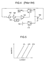
- the apparatus includes a monitor sensor 110, an amplifier 120, a comparator 130, current amplifiers 140 and 170 each for setting an amount of laser diode emission, a reference recording power value generator 150, a reference erasing power value generator 160, and a laser diode 180 playing the role of an optical head.
- the monitor sensor 110 senses the amount of emission from the laser diode or optical head 180 during recording.
- the output signal of the monitor sensor 110 is input to the amplifier 120 and amplified to a DC level necessary for control thereby.
- An amplified signal output from the amplifier 120 is fed to one input of the comparator 130.
- a reference recording power value output from the reference recording power value generator 150 is applied to the other input of the comparator 130.
- the comparator 130 compares the amplified signal and the reference recording power value and delivers the result of comparison to the current amplifier 140.
- Binary record data are also input to the current amplifier 140.
- a current set by the current amplifier 140 is output when the record data is, e.g., (logical) ONE "1", but it is not output when the record data is (logical) ZERO "0".
- the current set by the current amplifier 140 is fed to the laser diode 180.
- the reference erasing power value generator 160 feeds a constant current to the current amplifier 170.
- a current set by the current amplifier 170 is also input to the laser diode 180. In this manner, recording power and erasing power necessary for overwriting are delivered to the laser diode or optical head 180.
- Japanese Patent Laid-Open Publication No. 6-28676 discloses circuitry for controlling not only recording power but also erasing power.
- the circuitry includes a pin photodiode for sensing the output of a semiconductor laser and sets erasing power and recording power on the basis of the output of the pin photodiode.
- a sample-and-hold circuit holds the set erasing power and recording power and continuously applies them to the semiconductor laser until the end of recording and erasing operation.
- the circuitry may output adequate erasing power just after the start of a recording operation.
- the circuitry does not guarantee that the erasing power remains adequate despite the variation of ambient temperature that may occur after the start of recording.
- Japanese Patent Laid-Open Publication Nos. 4-362525, 7-262560 and 10-134352 also teach technologies of the kind described. None of them, however, teaches an implementation for maintaining the erasing power adequate against the varying ambient temperature.
- An optical recording/reproducing apparatus of the present invention includes a mean value detecting device for detecting a mean value in the binary modulation condition of the output of an optical head, a minimum value detecting device for detecting a minimum value in the binary modulation condition of the output of the optical head, and an input current setting device for setting a current to be input to the optical head in accordance with the above mean value and minimum value.
- the apparatus includes a monitor sensor 1, a narrow-band amplifier 2, a comparator 3, a current amplifier 4 for setting an amount of laser diode emission, a reference recording power value generator 5, a non-inverting wide-band amplifier 6, a signal generator 7 for DC offset adjustment, an inverting amplifier 8 with a DC offset adjuster, an envelope detector 9, an amplifier 10, a reference erasing power value generator 11, a comparator 12, a current amplifier for setting an amount of laser diode emission, and a laser diode or optical head 14.
- the monitor sensor 1 senses the amount of emission of the laser diode 14.
- the resulting output of the monitor sensor 1 is input to the narrow-band amplifier 2 and amplified to a DC level necessary for recording power control thereby.
- An amplified signal output from the narrow-band amplifier 2 is applied to the inverting input of the comparator 3.
- a reference recording power value output from the reference recording power generator 5 is applied to the non-inverting input of the comparator 3.
- the comparator 3 compares the amplified signal and reference recording power value and delivers the result of comparison to the current amplifier 4.
- Binary record data are also input to the current amplifier 4.
- a current set by the current amplifier 4 is output when the record data is "1", but it is not output when the record data is "0".
- an overwriting operation is effected during recording.
- the monitor sensor 1 senses the amount of optical head emission during recording.
- the resulting output of the monitor sensor 1 is input to the non-inverting wide-band amplifier 6.
- An amplified signal output form the amplifier 6 is delivered to the inverting input of the inverting amplifier 8 including the DC offset adjuster.
- a DC signal output from the signal generator 7 for DC offset adjustment is input to the non-inverting input of the inverting amplifier 8.
- the resulting output of the inverting amplifier 8 is fed to the envelope detector 9.
- the envelope detector 9 detects the envelope of the input signal and delivers its output to the amplifier 10.
- the amplifier 10 amplifies the output of the envelope detector 9 to a DC level necessary for erasing power control.
- the signal amplified by the amplifier 10 corresponds to a sensed erasing power value.
- the output of the amplifier 10 is input to the inverting input of the comparator 12.
- a reference erasing power value output from the reference erasing power value generator 11 is fed to the non-inverting input of the comparator 12.
- the comparator 12 compares the output of the amplifier 10 and the reference erasing power value and delivers the result of comparison to the current amplifier 13 which sets an amount of laser diode emission.
- the signal input to the current amplifier 13 and the signal input to the current amplifier 4 previously each are amplified by the respective amplifier and then fed to the laser diode 14 as a set current. In this manner, recording power and erasing power necessary for overwriting are input to the optical head.
- FIG. 2 shows the waveform of a signal A shown in FIG. 1 which is the signal input to the monitor sensor 1, i.e., the signal output from the laser diode 14, and the waveform of the output of the narrow-band amplifier 2 appearing at a point C also shown in FIG. 1.
- FIG. 1 shows the signal input to the monitor sensor 1, i.e., the signal output from the laser diode 14, and the waveform of the output of the narrow-band amplifier 2 appearing at a point C also shown in FIG. 1.
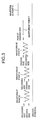
- FIG. 3 shows the waveform of the output of the monitor sensor 1 appearing at a point B, the waveform of the output of the non-inverting wide-band amplifier 6 appearing at a point D, the waveform of the output of the inverting amplifier 8 appearing at a point E, the waveform of the output of the envelope detector 9 appearing at a point F, and the waveform of the output of the amplifier 10 appearing at a point G.
- recording power control is executed with the mean value of the emission conditions. Therefore, the recording power output is input to and amplified by the narrow-band amplifier 2.
- erasing power control is executed with the peak values of the emission conditions. To detect peak values, the erasing power is input to and amplified by the non-inverting wide-band amplifier 6.
- the envelope detector 9 detects the envelope of the output of the wide-band amplifier while maintaining its waveform.
- the signal A has a sinusoidal waveform of positive potentials.
- the maximum value and minimum value of this waveform are respectively representative of the peak of the recording power and the peak of the erasing power.
- the waveform at the point C is representative of a DC signal having a negative potential. That is, the DC signal appearing at the point C is the mean value of the outputs of the monitor sensor 1 amplified and inverted by the narrow-band amplifier 2.
- the waveform at the point B is sinusoidal and has positive potentials like the signal A.
- the waveform at the point D is substantially identical with the waveform at the point B.
- the waveform at the point D differs in amplitude from the waveform at the point B because it is output from the non-inverting wide-band amplifier 6 that amplifies the signal appearing at the point B.
- the waveform at the point E is the inverted form of the waveform at the point D. Therefore, the maximum value and minimum value of the waveform at the point E are respectively representative of the peak value of the erasing power and the peak value of the recording power.
- the waveform at the point E has a value corresponding to the output of the signal generator 7 including the AD offset adjuster.
- the waveform at the point F is representative of DC having a positive potential. This is because the envelope detector 9 detects the envelope of the waveform at the point E and thereby causes the peak values at the erasure side to appear in the form of a continuous signal.
- the waveform at the point G is output from the amplifier 10 which DC amplifies the waveform at the point G.
- the illustrative embodiment senses the emission conditions of the laser diode 14 throughout the interval between the start of a recording operation and the end of the same so as to cause each of recording power and erasing power to constantly coincide with a particular reference value. It is therefore possible to maintain the output of the laser diode or optical head 14 at a value necessary for recording.
- an optical recording/reproducing apparatus includes mean value detecting means for detecting a mean value in the binary modulation condition of the output of an optical head, minimum value detecting means for detecting a minimum value in the binary modulation condition of the output of the optical head, and input current setting means for setting a current to be input to the optical head in accordance with the above mean value and minimum value.
- the apparatus is therefore capable of maintaining not only recording power but also erasing power at respective adequate values necessary for recording even when temperature around the apparatus varies. This allows a recording/reproducing error rate to be maintained.
Landscapes
- Physics & Mathematics (AREA)
- Optics & Photonics (AREA)
- Optical Head (AREA)
- Optical Recording Or Reproduction (AREA)
Abstract
Description
Claims (8)
- An optical recording/reproducing apparatus comprising:mean value detecting means for detecting a mean value in a binary modulation condition of an output of an optical head;minimum value detecting means for detecting a minimum value in the binary modulation condition of the output of said optical head; andinput current setting means for setting a current to be input to said optical head in accordance with the mean value and the minimum value.
- An apparatus as claimed in claim 1, wherein said input current setting means sets recording power of said optical head on the basis of the mean value.
- An apparatus as claimed in claim 1, said input current setting means sets erasing power of said optical head on the basis of the minimum value.
- An apparatus as claimed in claim 1, wherein said mean value detecting means comprises a narrow-band amplifier for amplifying the output of said optical head.
- An apparatus as claimed in claim 1, wherein said minimum value detecting means comprises:a non-inverting wide-band amplifier for amplifying an output of said optical head;an inverting amplifier for inverting an output of said non-inverting wide-band amplifier; andan envelope detector for detecting an envelope of an output of said inverting amplifier.
- An apparatus as claimed in claim 1, wherein said input current setting means comprises a comparator for comparing the mean value and a preselected recording power value and sets the recording power in accordance with a result of comparison output from said comparator.
- An apparatus as claimed in claim 1, wherein said input current setting means comprises a comparator for comparing the minimum value and a preselected reference erasing power value and sets the erasing power in accordance with a result of comparison output from said comparator.
- An apparatus as claimed in claim 1, wherein said apparatus records and reproduces data out of an overwritable optical recording/reproducing medium.
Applications Claiming Priority (2)
| Application Number | Priority Date | Filing Date | Title |
|---|---|---|---|
| JP6247999 | 1999-03-10 | ||
| JP11062479A JP2000260024A (en) | 1999-03-10 | 1999-03-10 | Optical recording and reproducing device |
Publications (2)
| Publication Number | Publication Date |
|---|---|
| EP1037205A2 true EP1037205A2 (en) | 2000-09-20 |
| EP1037205A3 EP1037205A3 (en) | 2001-01-10 |
Family
ID=13201375
Family Applications (1)
| Application Number | Title | Priority Date | Filing Date |
|---|---|---|---|
| EP00400625A Withdrawn EP1037205A3 (en) | 1999-03-10 | 2000-03-08 | Optical recording/reproducing apparatus |
Country Status (3)
| Country | Link |
|---|---|
| US (1) | US6556535B1 (en) |
| EP (1) | EP1037205A3 (en) |
| JP (1) | JP2000260024A (en) |
Families Citing this family (2)
| Publication number | Priority date | Publication date | Assignee | Title |
|---|---|---|---|---|
| US6980006B1 (en) * | 2001-01-22 | 2005-12-27 | Cadence Design Systems, Inc. | High speed envelope detector and method |
| KR100459702B1 (en) | 2002-02-22 | 2004-12-04 | 삼성전자주식회사 | Apparatus and method for controlling recording optical power in the optical driver |
Family Cites Families (15)
| Publication number | Priority date | Publication date | Assignee | Title |
|---|---|---|---|---|
| US4685097A (en) * | 1985-07-25 | 1987-08-04 | Laser Magnetic Storage International Company | Power control system for a semiconductor laser |
| JPH07111782B2 (en) * | 1986-08-13 | 1995-11-29 | ソニー株式会社 | Optical disc recording / reproducing device |
| JP2687544B2 (en) * | 1989-02-01 | 1997-12-08 | 日本電気株式会社 | Optical recording / reproducing device |
| JPH04157632A (en) * | 1990-10-20 | 1992-05-29 | Ricoh Co Ltd | Semiconductor laser drive circuit |
| JPH04362525A (en) | 1991-06-07 | 1992-12-15 | Ricoh Co Ltd | Optical disc recording/playback device |
| US5260956A (en) | 1991-09-30 | 1993-11-09 | Nikon Corporation | Laser drive circuit |
| JPH0628676A (en) | 1992-07-13 | 1994-02-04 | Matsushita Electric Ind Co Ltd | Optical disk device |
| JP3477770B2 (en) * | 1992-12-16 | 2003-12-10 | 松下電器産業株式会社 | Laser power control device and control method |
| US5768245A (en) | 1993-12-27 | 1998-06-16 | Fujitsu Limited | Optical disk apparatus |
| JPH07262560A (en) | 1994-03-24 | 1995-10-13 | Toshiba Corp | Recording / playback device |
| US5648952A (en) * | 1994-09-28 | 1997-07-15 | Ricoh Company, Ltd. | Phase-change optical disc recording method and apparatus, and information recording apparatus and recording pre-compensation method |
| JP3441212B2 (en) | 1995-01-19 | 2003-08-25 | 株式会社リコー | Power control method |
| JPH09107144A (en) * | 1995-10-11 | 1997-04-22 | Sony Corp | Laser diode deterioration judgment circuit |
| JPH10134352A (en) | 1996-10-31 | 1998-05-22 | Ricoh Co Ltd | Optical disk drive |
| JPH11144288A (en) * | 1997-11-05 | 1999-05-28 | Yamaha Corp | Laser power control method for optical disk recording and laser diode driving circuit for optical disk recorder |
-
1999
- 1999-03-10 JP JP11062479A patent/JP2000260024A/en active Pending
-
2000
- 2000-03-08 US US09/520,510 patent/US6556535B1/en not_active Expired - Fee Related
- 2000-03-08 EP EP00400625A patent/EP1037205A3/en not_active Withdrawn
Also Published As
| Publication number | Publication date |
|---|---|
| EP1037205A3 (en) | 2001-01-10 |
| US6556535B1 (en) | 2003-04-29 |
| JP2000260024A (en) | 2000-09-22 |
Similar Documents
| Publication | Publication Date | Title |
|---|---|---|
| US5436880A (en) | Laser power control in an optical recording system using partial correction of reflected signal error | |
| EP0314390B1 (en) | Semiconductor laser control circuit | |
| US7760597B2 (en) | Optimal recording apparatus and method for determining an optical recording condition | |
| US7778127B2 (en) | Optimal recording method for optical recording media and optical recording medium stored with information about optimum recording conditions | |
| US20040027949A1 (en) | Information recording method and information recording apparatus | |
| JPH06267008A (en) | Recording device of information signal to magnetic recording carrier | |
| US4663555A (en) | Method and apparatus for controlling a bimorph leaf which supports a deflectable head | |
| US6556535B1 (en) | Optical recording/reproducing apparatus | |
| US6798728B2 (en) | Optical disk device and luminescent power control method for semiconductor laser | |
| WO2003021584A1 (en) | Method and device for running optimum power control | |
| KR19980078070A (en) | Optical record and playback device for optimal recording power control | |
| KR100446307B1 (en) | Automatic power calibration apparatus for optical recording device, and the method thereof | |
| US6438077B1 (en) | Optical disk unit | |
| WO2003065357A3 (en) | Record carrier, device and method for scanning the record carrier | |
| JP3257287B2 (en) | Optical disk recording device | |
| US6754156B2 (en) | Recording apparatus for use with optical recording medium and method thereof | |
| EP1098305A3 (en) | Optical disk recording/reproducing device employing waveform correction of laser output signal | |
| JPH10134352A (en) | Optical disk drive | |
| JPH01173477A (en) | Information recording and reproducing device | |
| JPH0945982A (en) | Laser drive | |
| JP2002334440A (en) | Optical recording / reproducing device | |
| JPH0636327A (en) | Optical disk device | |
| JPS6260129A (en) | optical recording and reproducing device | |
| JPH07153106A (en) | Optical disk device | |
| JPH04134639A (en) | Laser power generator |
Legal Events
| Date | Code | Title | Description |
|---|---|---|---|
| PUAI | Public reference made under article 153(3) epc to a published international application that has entered the european phase |
Free format text: ORIGINAL CODE: 0009012 |
|
| AK | Designated contracting states |
Kind code of ref document: A2 Designated state(s): FR NL |
|
| AX | Request for extension of the european patent |
Free format text: AL;LT;LV;MK;RO;SI |
|
| PUAL | Search report despatched |
Free format text: ORIGINAL CODE: 0009013 |
|
| AK | Designated contracting states |
Kind code of ref document: A3 Designated state(s): AT BE CH CY DE DK ES FI FR GB GR IE IT LI LU MC NL PT SE |
|
| AX | Request for extension of the european patent |
Free format text: AL;LT;LV;MK;RO;SI |
|
| 17P | Request for examination filed |
Effective date: 20010630 |
|
| AKX | Designation fees paid |
Free format text: AT BE |
|
| REG | Reference to a national code |
Ref country code: DE Ref legal event code: 8566 |
|
| RBV | Designated contracting states (corrected) |
Designated state(s): FR NL |
|
| GRAP | Despatch of communication of intention to grant a patent |
Free format text: ORIGINAL CODE: EPIDOSNIGR1 |
|
| STAA | Information on the status of an ep patent application or granted ep patent |
Free format text: STATUS: THE APPLICATION IS DEEMED TO BE WITHDRAWN |
|
| 18D | Application deemed to be withdrawn |
Effective date: 20080619 |