EP1037054B1 - Elementary low loss calibrating structure for calibrating an integrated circuit probe - Google Patents
Elementary low loss calibrating structure for calibrating an integrated circuit probe Download PDFInfo
- Publication number
- EP1037054B1 EP1037054B1 EP00430005A EP00430005A EP1037054B1 EP 1037054 B1 EP1037054 B1 EP 1037054B1 EP 00430005 A EP00430005 A EP 00430005A EP 00430005 A EP00430005 A EP 00430005A EP 1037054 B1 EP1037054 B1 EP 1037054B1
- Authority
- EP
- European Patent Office
- Prior art keywords
- standard
- probe
- circuit
- circuits
- integrated circuit
- Prior art date
- Legal status (The legal status is an assumption and is not a legal conclusion. Google has not performed a legal analysis and makes no representation as to the accuracy of the status listed.)
- Expired - Lifetime
Links
Images


Classifications
-
- G—PHYSICS
- G01—MEASURING; TESTING
- G01R—MEASURING ELECTRIC VARIABLES; MEASURING MAGNETIC VARIABLES
- G01R35/00—Testing or calibrating of apparatus covered by the other groups of this subclass
- G01R35/005—Calibrating; Standards or reference devices, e.g. voltage or resistance standards, "golden" references
-
- G—PHYSICS
- G01—MEASURING; TESTING
- G01R—MEASURING ELECTRIC VARIABLES; MEASURING MAGNETIC VARIABLES
- G01R1/00—Details of instruments or arrangements of the types included in groups G01R5/00 - G01R13/00 and G01R31/00
- G01R1/28—Provision in measuring instruments for reference values, e.g. standard voltage, standard waveform
-
- H—ELECTRICITY
- H01—ELECTRIC ELEMENTS
- H01L—SEMICONDUCTOR DEVICES NOT COVERED BY CLASS H10
- H01L2224/00—Indexing scheme for arrangements for connecting or disconnecting semiconductor or solid-state bodies and methods related thereto as covered by H01L24/00
- H01L2224/01—Means for bonding being attached to, or being formed on, the surface to be connected, e.g. chip-to-package, die-attach, "first-level" interconnects; Manufacturing methods related thereto
- H01L2224/02—Bonding areas; Manufacturing methods related thereto
- H01L2224/04—Structure, shape, material or disposition of the bonding areas prior to the connecting process
- H01L2224/05—Structure, shape, material or disposition of the bonding areas prior to the connecting process of an individual bonding area
- H01L2224/0554—External layer
- H01L2224/0555—Shape
- H01L2224/05552—Shape in top view
- H01L2224/05554—Shape in top view being square
-
- H—ELECTRICITY
- H01—ELECTRIC ELEMENTS
- H01L—SEMICONDUCTOR DEVICES NOT COVERED BY CLASS H10
- H01L2224/00—Indexing scheme for arrangements for connecting or disconnecting semiconductor or solid-state bodies and methods related thereto as covered by H01L24/00
- H01L2224/01—Means for bonding being attached to, or being formed on, the surface to be connected, e.g. chip-to-package, die-attach, "first-level" interconnects; Manufacturing methods related thereto
- H01L2224/02—Bonding areas; Manufacturing methods related thereto
- H01L2224/04—Structure, shape, material or disposition of the bonding areas prior to the connecting process
- H01L2224/06—Structure, shape, material or disposition of the bonding areas prior to the connecting process of a plurality of bonding areas
Definitions
- the present invention relates to the electrical test of so-called "RF" integrated circuits, with inputs or outputs provided for receiving or delivering signals alternatives in the field of radio frequencies.
- the present invention relates more particularly to electrical test of RF integrated circuits present on a silicon wafer, commonly called "wafer", before the cutting of the wafer into individual components.
- Figure 1 represents a wafer of silicon 1 on which has been made, by photolithography, a large number of integrated circuits 2 of same structure.
- an integrated circuit 2 has an active zone 3 and connection pads 4 electrically connected to the area active 3.
- Higher magnification of the active zone 3 would show hundreds or even thousands of integrated components together forming various functions electronic devices to be tested.
- the circuit electrical test integrated 2 still present on the wafer 1 to identify and to reject defective integrated circuits or those that do not present the expected characteristics, before the wafer cutting and assembly of integrated circuits individualized in a housing or their assembly on a interconnect support. This operation is therefore essential for reducing production costs, especially in the context of mass production.
- Figure 3 very schematically represents a system conventional wafer integrated circuit test, comprising a test station 11 connected to a probe 12 by through a bundle of electrical cables 13.
- the probe 12 is a printed circuit board 14 provided with metal tips arranged to coincide with the connection pads of an integrated circuit 2.
- the wafer 1 is disposed on a plate 16 movable in the horizontal plane and the integrated circuits are tested one after the other, by movements and movements of lifting and The entire system is piloted by a test program loaded into a memory 17, which determines the electrical characteristics of the signals of test to be applied to integrated circuits and the measurements to be carry out.
- This conventional method of testing integrated circuits in means of a probe constituted by a spiked card finds its limits when one wants to test RF integrated circuits comprising RF inputs / outputs requiring measurement frequencies ranging from a few hundred MegaHertz to some Gigahertz.
- These include integrated circuits with analog modulation functions and demodulation, mixers, amplifiers, filters, voltage controlled oscillators (VCOs), phase-locked loops (PLL) ..., intended for radio, television, radio receivers GPS receivers ...
- VCOs voltage controlled oscillators
- PLL phase-locked loops
- electrical signals have short wavelengths and we see appear in the probe 12 and in the drivers 13 connecting the probe to the test station 11 various phenomena of reflection and phase rotation that distort the measurements by creating interferences and changes in electrical levels.
- the tracks copper of the printed circuit board 14 and the tips 15 of the probe 12 have capacitances and inductances not insignificant parasites.
- RF probes satisfactory characteristics at high frequency.
- Cascade TM Microtech located at Oregon 97005, USA, proposes RF points ("transmission line probes") of reference “Air Coplanar” and membrane probes ("RFIC membrane probe cards ”) with HF conductors at microstrip (microstrip) and Nickel contact balls ("contact bumps").
- Such probes offer a band passing several tens of GigaHertz, a weak reflection coefficient S11 and a coefficient of S12 transmission with attenuation lower than 3dB (Cf. presentation of Cascade TM products on http // www.cmicro.com).
- the OSL method consists of carry out three measurements applying successively to the output of the probe at least three standard loads, in general infinite impedance (open circuit), zero impedance (short circuit), an impedance of 50 ⁇ (load).
- the network analyzer determines the parameters "S" of the probe and the test station performs, during subsequent measurements, automatic error correction to compensate for the influence of these parameters for obtaining accurate and reliable measurements.
- the standard loads used are thin layers on a ceramic substrate, calibrated by a National Metrology Laboratory.
- the RF points of the "Air Coplanar" type require manual adjustment of spike orientation and remain reserved for laboratory measurements or small productions.
- Membrane probes with balls of contact although specially designed for the test of integrated circuits on wafer, require to be calibrated the use of specific thin-layer standard circuits a high cost price. For various other reasons practices, the applicant considers that the probes membranes are not suitable for mass production of integrated circuits that can represent several million rooms.
- the tips or probes contact balls are forcefully applied on the connection ranges of the standard circuits, so that breaking a surface layer of oxide forming on contact air and establish a good electrical contact ("welding
- the thin-film standard circuits in addition to their high price, are therefore subject to wear and have a low lifetime.
- the thin-film standard circuits do not do not have the same thickness as silicon wafers and require for their installation a setting of the plateau 16 ( Figure 3) necessarily followed by another adjustment of the tray at the time of installation of the wafer.
- This inconvenience is compounded with the fact that RF probes require several calibrations during the test of a batch of fleas. These various calibrations involve the intervention of a qualified engineer and represent 5 to 10% of the time spent to the electrical test.
- a general objective of the present invention is to provide a method for calibrating an RF probe that is suitable for mass production, economical, simple to put implemented while being accurate and reliable, and who can may be implemented by unqualified personnel.
- a more particular object of the present invention is to provide a standard circuit which is of a low price of returns and simplifies calibration of a circuit probe RF integrated.
- a standard circuit comprising a plurality of elementary standard structures having standard charges of the same type, arranged in such a way as to have corresponding contact areas by their location to RF connection pads of the integrated circuit to test.
- the standard circuit includes a non-volatile memory connected to corresponding contact by their location to beaches of non-RF connection of the integrated circuit to be tested.
- a plate is also produced of silicon comprising a plurality of standard circuits according to the invention, or comprising both circuits integrated test and standard circuits according to the invention.
- each standard structure may be delimited laterally by engraving, or by furrows practiced in the substrate.
- one of the contact pads of a structure elementary standard is connected to the driver screen.
- an elementary standard structure may include two series standard loads connected by their point middle to the driver screen.
- a standard structure can also include at least one contact area to access in the middle point of the two standard loads.
- a standard load can be an open circuit formed by two sections of tracks conductors do not meet, a short circuit between two sections of conductive tracks, a resistive element connecting two sections of conductive tracks, or a capacity comprising a conductive plate deposited on the insulating layer and overhanging the buried conductor screen.
- RF integrated circuits are also realized comprising at least one conductive screen buried under two RF connection pads.
- the screen conductor may be delimited laterally by etching, or by grooves made in the circuit substrate integrated.
- a calibration method according to the invention of a test probe of an RF integrated circuit includes a step of determining the characteristics of the RF transmission lines of the probe made by means of a network analyzer and standard circuits according to the invention present on a silicon wafer.
- the present invention also relates to a method of electrical test of an RF integrated circuit present on a silicon wafer, by means of a test station provided with RF ports, a network analyzer and a probe, comprising a step of determining RF characteristics of the probe carried out by means of standard circuits according to the present invention on a silicon wafer, the RF characteristics of the probe being used as terms patches during the electrical test of the integrated circuit.
- the general objective of the invention is to perform the circuit electrical test embedded RF on silicon wafer in an environment industrial, in a simple, fast and inexpensive way by obtaining accurate and reliable measurements.
- the current invention includes various aspects that will be described each independently of each other.
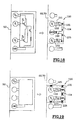
- the electrical test of RF integrated circuits is carried out at by means of a probe 20 comprising a printed circuit 21 provided 22.
- the printed circuit board is shaped ring and the points 22, oriented towards the center of the structure, are arranged to coincide with the connection pads of an integrated circuit 50.
- the probe 20 is similar in structure to conventional circuit probes printed but has RF transmission lines offering satisfactory characteristics at high frequency. As as we will see later, these characteristics will be measured in the form of "S" parameters and compensated by the techniques classic error correction.
- the probe 20 constitutes an alternative to HF membrane probes, optional but advantageous in terms of flexibility of use and price cost, for measuring frequencies falling within the low of the RF range, ranging from a few hundred megahertz to some GigaHertz. Most RF ICs current operating in this frequency range, the probe 20 can cover almost all needs industrial.
- the printed circuit 21 is a multilayer circuit preferably having a ground plane 23 buried and uninterrupted, metallized crossings 24 to connect the various conductive levels, and RF-type connectors.
- the tips 22, of a short length of the order of 3 to 9 mm, are soldered by their base on the printed circuit 21 and are held by an electrically insulating piece 29 forming a kind of ring extending under the printed circuit 21.
- the printed circuit 21 has on its two faces of passive components 26, 27 as capabilities and inductors, allowing to match the impedances of transmission lines of the probe 20 connecting the connectors 25 to the spikes 22.
- the printed circuit 21 also includes transformers 28, for delivering symmetrical signals to test the differential inputs of a circuit integrated.
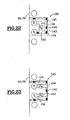
- Figure 6 shows the diagram of an embodiment of a line of transmission 30 provided for testing inputs differential of an integrated circuit ("balanced inputs").
- the line 30 comprises two conductive tracks 31, 32 of the circuit printed 21 leading to two points 22-1, 22-2.
- Tracks 31, 32 are connected to the terminals of the secondary coil of a transformer 28 whose midpoint is connected to the mass, the primary coil of the transformer being connected to a connector 25.
- the tracks 31, 32 each comprise a tuning capacity Ca1, Ca2 in series and are connected by a chord inductance La1.
- Capacities Ca1, Ca2 and the inductance La1 make it possible to compensate the influence parasitic elements present in the transmission line 30, in particular a parasitic capacitance Cp1 present between the transformer primary 27 and mass, capabilities parasites Cp2, Cp3 present between each terminal of the secondary and the mass, parasitic capacitances Cp4, Cp5 present between each point 22-1, 22-2 and the mass, and the inductances parasites Lp1, Lp2 of the points 22-1, 22-2. More particularly, the Ca1, Ca2 and inductance La1 make it possible to adjust the frequency of resonance of the transmission line 30 so that the probe 20 behaves like a "transparent window" allowing access to an integrated circuit.
- FIG. 7 shows the diagram of an embodiment of a line of unsymmetrical transmission 40 intended to test inputs unipolar of an integrated circuit ("single-ended inputs").
- the transmission line 40 includes a phase track 41 (signal) and a ground track 42 (reference) leading to points 22-3, 22-4.
- the tracks of phase 41 and mass 42 each have a Ca 3, Ca 4 series and are connected to ground by a La2 inductor, A3.
- these components make it possible compensate for the influence of parasitic elements Lp1, Lp2, Cp6 present in the transmission line.
- the coefficients S12 and S21 are considered equal.
- the "S" parameters of each of the lines RF transmission of the probe 20 will be determined at means of a network analyzer, after three measurements requiring to successively connect the spikes 22 to minus three standard loads Z1, Z2, Z3.
- the problem posed the calibration of the probe 20, and generally the calibration of an RF probe intended to be applied on a integrated circuit, is essentially practical and is related to number of transmission lines to be calibrated, and that multiple recalibrations are necessary during electrical test of a batch of integrated circuits.
- FIG. 9A represents a circuit integrated 50 having an active area 51 and ranges of aluminum connection.
- connection pads P1, P2, P3 ... P12 corresponding to RF inputs / outputs of the integrated circuit.
- These inputs / outputs can be of unipolar type ("single-ended") or of balanced type.
- Others connection pads, not referenced in the figure, are "non-RF" connection pads corresponding to I / O low frequency (logic signals) or current continuous (bias voltages, supply voltages, etc.).
- FIG. 9B represents a standard circuit 60 according to the invention, made on a silicon substrate.
- the circuit 60 is a kind of dummy integrated circuit 50 not including the active area 51, in which there are the RF and non-RF connection pads of the integrated circuit 50.
- the connection pads P1 to P12 corresponding to the RF ranges of same reference of the circuit 50, are connected two by two to an elementary standard charge, respectively Z 1,2 , Z 3,4 , Z 5,6 , Z 7,8 , Z 9,10 , Z 11,12 .
- Non-RF ranges remain without connection.
- Each pair of tracks P1 / P2, P3 / P4,... P11 / P12 thus forms, with the reference charge Z associated therewith, an elemental reference structure on a silicon substrate, examples of which will be described below.
- FIG. 9C represents a variant embodiment in which the standard circuit, referenced 70, comprises in in addition to an active area 71 connected to the non-RF ranges.
- the area active 71 is a remanent type memory, for example a EEPROM memory comprising floating gate transistors, to store the values of standard loads elementary Z present across the RF ranges P1 to P12.
- the invention it is carried out on a silicon wafer at least three standard circuits 60 differing by the characteristic impedance of the Z standard loads they behave.
- the first standard circuit type "O" ("Open")
- the second circuit standard type “S” (“Short”)
- the third standard circuit of type "L” (“Load”)
- circuits are also provided.
- type "C1” and type “C2” standards, in which the Z loads are capacitors or inductances.
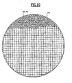
- Figures 10 and 11 illustrate two modes of realization of a wafer according to the invention.
- the wafer 75 includes only standard circuits 60 or 70 of type “O", “S”, “L”, “C1” and “C2" succeeding each other others and occupying all the useful surface of the wafer.
- the wafer 76 is a "production” wafer comprising integrated circuits 50 to be tested and marketed, as well as some 60 or 70 standard circuits arranged in place of certain integrated circuits 50.
- the wafer 76 has two rows five standard circuits of type "O", “S", “L” "C1” and “C2, taking the place of ten integrated circuits 50.
- circuits are thus available standards 60 or 70 (FIGS. 9B, 9C) of the same shape and likewise the size of the integrated circuits 50 to be tested (FIG. 9A), arranged on a wafer 75 of the same thickness as the wafer "production” ( Figure 10) or on the “production” wafer 76 itself ( Figure 11).
- These standard circuits include elementary standard structures with contact pads coinciding with the tips of the probe 20 ( Figure 4), dedicated to the electrical test of integrated circuits 50. As we will see below, these basic elementary structures go serve as "transfer standards" for bring them to the production sites, where the electrical test of integrated circuits is realized, a calibration reference given by calibrated thin-layer ceramic circuits by a national metrology laboratory.
- two RF peaks are calibrated 80 by means of a measuring bench 81 and a circuit 82 to thin layers having standard structures 83, 84, 85 type "O", "S", “L” calibrated by an approved laboratory.
- the tips 80 are for example Cascade TM Microtech tips the "Air Coplanar” series.
- the measuring bench 81 is provided with a conventional network analyzer, commonly available in the trade. The "S" parameters measured by the analyzer of network are used to calibrate the measurement system to the tips of the tips 80.
- the wafer 75 (FIG 10) is placed on the worktable and the RF peaks 80 measure the electrical characteristics of each elementary standard structure of each standard circuit 60 present on the wafer.
- the measurement is made at several frequencies, for example five frequencies, chosen according to the nominal frequency F0 of the integrated circuits to be tested later. For example, frequencies of 780, 790, 800, 810 and 820 MHz are chosen for integrated circuits having a nominal frequency of 800 MHz.
- the measurement bench 81 delivers the results of the measurements to a computer 86. These results are recorded on a support 87, for example a diskette, which will later accompany the wafer 75 on a production site.
- FIG. 14 schematically illustrates a variant of the calibration step in which the standard circuits 70 present on the wafer 75 each comprise a non-volatile memory 71, as described above in relation with FIG. 9C.
- the files containing the values of the elementary standard charges Z 1.2 .... Z 11.12 are stored in the memory 71 instead of being recorded on a diskette.
- the programming of the memory is done in a conventional manner, by means of a programmer 88 receiving the values to be recorded from the computer 86.
- the programmer 88 is connected to the non-RF contact pads of the circuit 70 by means of spikes 89.
- the standard wafer 75 is sent to a production site, which can be located thousands of kilometers from the place where it was calibrated.
- a production site which can be located thousands of kilometers from the place where it was calibrated.
- the probe 20 is connected to the RF and non-RF ports of the station 90 by coaxial cables or other types of cables.
- the cables connected to the RF ports are previously calibrated by the OSL method using standard commercially available loads.
- the probe 20 is calibrated by means of three standard circuits 60, 70 of type "O", "S” and "L" selected on the wafer 75 from the set of available standard circuits.
- the standard circuits are used only a specified number of times, for reasons relating to the degradation of the contact pads by the test points and the search for an optimal electrical contact.
- the values of the elementary standard impedances Z 1.2 , Z 3.4 ... Z 11.12 are given by the diskette 87 ( Figure 13) or are read directly into the integrated memory 71, by means of the probe 20.
- the data can also be transmitted via a computer network.
- the probe 20 is applied successively to three standard circuits, and station 90 measures the reflection coefficients ⁇ n of the various lines of RF transmission of the probe.
- the network analyzer of station 90 is able to determine the "S" parameters of the RF transmission lines of the probe. These parameters are kept in memory as corrective parameters of measurements made later during the electrical test of RF integrated circuits present on a "production" wafer.
- the calibration method according to the invention is simple and quick to implement. It only requires installing the wafer 75 on the test tray ("chuck") and the successive positioning of the probe 20 on three standard circuits.
- the process of the invention can be fully automated, and does not require intervention a qualified RF engineer.
- complementary standard circuits of type "C1" and “C2" verify the correct calibration of the probe and detect an isolated error. If the impedance values of "C1" and “C2" circuits measured with probe 20 do not do not correspond to the values given by the measuring bench reference number (FIG. 13 or 14), a signal can be generated alarm to make an operator intervene. The operator is going carry out a cleaning of the probe or a new calibration.
- FIG. 16A shows a sectional view of an "O" type elementary standard structure 100 (open circuit) produced on a silicon substrate 101, in particular a silicon wafer.
- the structure 100 comprises two contact pads 102, 103 deposited on the substrate 101 via an electrically insulating layer 104, for example silicon oxide. It is assumed here that the substrate is placed on a metal plate 105 connected to the ground.
- the application of a VRF voltage between the range 102 and the range 103 reveals an electric field E which radiates in the thickness of the substrate 101 and causes the standard structure to exhibit electrical losses.
- 16B shows that the ranges 102, 103, between which there is a resistor R0 representing the open circuit, are connected to the ground via a circuit C, R, L comprising a parasitic capacitance Cs1, the electrical resistance Rs1 of the substrate and a leakage inductance Ls1 of the metal plate 105 connected to the test equipment.
- the capacity Csl is of high value because its armatures are formed by the whole surface of the substrate, which extends well beyond the standard structure.
- Figure 17A is a sectional view of a structure 110 according to the invention, which differs from the previous in that a conductive screen 106 is buried under the oxide layer 104.
- the screen 106, metal, silicon polycrystalline or highly doped silicon is connected to the 104 (mass) by a conductive port 107 passing through the oxide layer, filled with metal or silicon strongly dope.
- the screen 106 extends over a limited area with regard to the surface of the substrate but underlie the whole area occupied by the standard structure, so that the beaches of contact 102, 103 overhang the screen 106.
- the field electrical E is confined between the range 102 and the screen 106 and electrical losses are diminished.
- FIG. 17B shows that the beach 102 is isolated from the substrate 101 and the metal tray 105.
- Beach 103 remains connected to the ground via Cs2 capacity, Rsl resistance and inductance Lsl of the metal tray 105.
- the capacity Cs2 is much lower than the capacity Csl of Figure 16B because its frames are defined by the size of the screen 106, which is much lower than that of the substrate.
- the standard structure 110 is therefore more satisfactory than the structure 100.
- Figures 18 and 19 show two structures elementary standards 120, 130 (right portion of the figures) and the initial arrangement of the connection pads on the circuit integrated 50 (left side of the figures).
- These structures standards 120, 130 are symmetrical and intended for the calibration of symmetrical transmission lines (figure 6), making it possible to test differential inputs of the integrated circuit. At the time of calibration of the probe, structures 120, 130 will thus receive a symmetrical signal.
- the "Air Coplanar" type RF tips used for calibrating the standard structures can not perform differential mode measurements, for reasons inherent to their HF structure.
- the standard structures 120, 130 solve this drawback, as we will see him now.
- the integrated circuit 50 for example includes a Vcc power supply range, a range GND, and two ranges P1, P2 corresponding to one differential input, schematically represented by a mounting two transistors T1, T2 to common emitter.
- the basic standard structure 120 includes the two ranges P1, P2 and is delimited by a conductive screen 121 buried under an insulating layer, including the edges are materialized by dashed lines.
- the P1, P2 are each connected to a load Z1, Z2 by sections of conductive tracks 122, 123.
- Charges Z1, Z2 are represented as a shape location square that can be left empty (open circuit) or receive a conductive material, for example an aluminum deposit of particular shape, wide or narrow (short circuit or resistance), or a resistive material such as doped silicon (resistance).
- the charges Z1, Z2 are connected to each other by a third section of track 124.
- the track section 124 is itself connected to the screen 106 by various conductive orifices 125 passing through the insulating layer.
- section 124 is extended in its central part in the form of an arm 126 leading to a GNDV virtual mass range, arranged between the beaches P1, P2, in alignment with the latter.
- the load Z1 is first measured by placing the points (80) on the P1 and GNDV ranges. We then measure the Z2 load via the P2 and GNDV ranges. The elementary standard charge for the calibration of a line of differential transmission is calculated by doing the sum two charges Z1 and Z2.
- the elementary structure 130 of FIG. distinguished from the structure 120 by the fact that two ranges of virtual mass GNDV1, GNDV2 are arranged in relation to P1 and P2, on the other side of the charges Z1, Z2, the P1 and P2 ranges being too close to each other for allow insertion of a measuring range.
- the section of track 124 connects the GNDV1, GNDV2 and extends beyond of these to follow the area occupied by the screen 121 and guarantee a good connection to the latter, thanks to various conducting orifices 125.
- the load Z1 is measured between the ranges P1 and GNDV1 and the load Z2 is measured between the P2 and GNDV2 ranges.
- Fig. 20 shows a symmetrical standard structure 160 of type "C1" or “C2".
- This structure looks like strongly to an "S" type structure that would be realized in accordance with Figure 18, the elementary charges being formed by squares of conductive material, or plates 161, 162, connected to the ranges P1, P2.
- the plates 161, 162 do not come into contact with the section of central track 163 (runway section 163, connected to the buried screen 164, is preserved because the structure 160 is performed in the same way as a structure of type "O", "S” or “L”).
- the plates 161, 162 form with the buried driver screen 164 two capacitors in series Ca, Cb.
- the total impedance of structure 160 is a capacitor whose value depends on the size of the plates 161, 162.
- Figure 22 shows a standard structure elementary element 140 of unsymmetrical type, in which the P1 range is intended to receive the phase and the range P2 to receive the mass of a measurement signal.
- the P1 range is connected to a load Z3 by a section of track 141 and the P2 range is connected to the other end of the Z3 load by a section of runway 142.
- Runway section 142 is connected to a buried driver screen 143 via of conducting orifices 144, arranged in particular along a arm 145 along the area occupied by the screen 143.
- Figure 23 shows a symmetrical structure 150 in which the range P1 is connected by a section of track 151 to a Z4 load and the P2 range is connected by a track section 152 at a load Z5.
- a section of track 153 connects the charges Z4, Z5 whose sum forms the impedance standard.
- the track section 153 is connected to a buried screen 154, by orifices 155.
- the screen 154 thus forms a virtual mass, although the structure does not has no virtual mass range.
- Non-capacitive type capacitive structures symmetric can also be achieved by following the teaching of Figure 20, charges Z3, or Z4 and Z5 then taking the form of conductive plates connected only at P1, P2.
- structures inductive effects can be achieved by means of metal shaped flat coils.
- the standard structures according to the invention are preferably made using the same technology than the corresponding integrated circuit.
- the technology called "HSB2" High Speed Bipolar
- HSD2 High Speed Bipolar
- furrows are practiced all around each standard structure according to the invention for cutting the buried conductive layer, and show under each elemental structure a conductive screen insulated from the rest of the conductive layer.
- a another embodiment, in itself more conventional, is to burn the buried layer before the deposit of the oxide layer, so that only the conductive screens.
- a standard circuit according to the invention has electrical properties that are as close as possible to those of the integrated circuit to be tested. So, he enters the of the present invention to provide circuits integrated circuits, for example the circuit 50 of FIG. 9A, having under each pair of RF ranges a conductive screen.
- the forecasting such a screen can only improve the performance of the high-frequency circuit, reducing its electrical losses.
- the screen is arranged as illustrated by one of FIGS. 18 to 23, according to which the tracks of the circuit integrated correspond to symmetrical inputs / outputs or unsymmetrical.
- the screen can be connected to the range of mass in the case of an unsymmetrical input.
- the screen In the case of a differential input, the screen can be connected to the midpoint of the load seen from the connection pads. This midpoint is for example the connection point of the transmitters of transistors T1, T2 shown in FIG. 18.
- the first aspect of the invention relates to the use of optional RF probe made from a circuit printed, replacing conventional membrane probes.
- the second aspect relates to the realization of circuits standards on silicon with coinciding contact pads with the connection pads of an integrated circuit to be tested and, therefore, with the tips or the balls of contact a probe for testing the integrated circuit.
- the third aspect of the invention relates to the calibration a test probe by means of these standard circuits, used as transfer standards.
- the fourth aspect of the invention relates to the production of structures Low-loss silicon standards with a display buried, and to the generalization of the screen buried at RF integrated circuits themselves.
- the fifth aspect of the invention relates to embodiments of elementary standard structures, including structures symmetrical with additional contact areas to be calibrated with unsymmetrical RF tips. he it will be clear to those skilled in the art that these various aspects of the invention are independent of one another, although their combination forms an advantageous whole to achieve in the most direct way the general objective of the invention.
Landscapes
- Physics & Mathematics (AREA)
- General Physics & Mathematics (AREA)
- Testing Or Measuring Of Semiconductors Or The Like (AREA)
- Testing Of Individual Semiconductor Devices (AREA)
- Semiconductor Integrated Circuits (AREA)
Description
La présente invention concerne le test électrique de circuits intégrés dits "RF", comportant des entrées ou des sorties prévues pour recevoir ou délivrer des signaux alternatifs dans le domaine des radiofréquences.The present invention relates to the electrical test of so-called "RF" integrated circuits, with inputs or outputs provided for receiving or delivering signals alternatives in the field of radio frequencies.
La présente invention concerne plus particulièrement le test électrique des circuits intégrés RF présents sur une plaquette de silicium, communément appelée "wafer", avant la découpe de la plaquette en composants individuels.The present invention relates more particularly to electrical test of RF integrated circuits present on a silicon wafer, commonly called "wafer", before the cutting of the wafer into individual components.
Pour fixer les idées, la figure 1 représente un wafer
de silicium 1 sur lequel a été réalisé, par
photolithographie, un grand nombre de circuits intégrés 2 de
même structure. Sur la vue agrandie de la figure 2, il
apparaít qu'un circuit intégré 2 présente une zone active 3
et des plages de connexion 4 reliées électriquement à la zone
active 3. Un plus fort grossissement de la zone active 3
ferait apparaítre des centaines voire des milliers de
composants intégrés formant ensemble diverses fonctions
électroniques devant être testées.To fix ideas, Figure 1 represents a wafer
of
Les rendements de fabrication des circuits intégrés
étant inférieurs à 100%, le test électrique des circuits
intégrés 2 encore présents sur le wafer 1 permet d'identifier
et de rejeter les circuits intégrés défectueux ou ceux qui ne
présentent pas les caractéristiques attendues, avant la
découpe du wafer et le montage des circuits intégrés
individualisés dans un boítier ou leur assemblage sur un
support d'interconnexion. Cette opération est donc
essentielle pour la diminution des coûts de production,
notamment dans le cadre d'une production de masse.Manufacturing efficiencies of integrated circuits
being less than 100%, the circuit electrical test
integrated 2 still present on the
La figure 3 représente très schématiquement un système
classique de test de circuits intégrés sur wafer, comprenant
une station de test 11 reliée à une sonde 12 par
l'intermédiaire d'un faisceau de câbles électriques 13. La
sonde 12 est une carte à circuit imprimé 14 pourvue de
pointes métalliques 15 agencées pour coïncider avec les
plages de connexion d'un circuit intégré 2. Le wafer 1 est
disposé sur un plateau 16 mobile dans le plan horizontal et
les circuits intégrés sont testés les uns après les autres,
par des déplacements et des mouvements de levée et de
descente du plateau 16. L'ensemble du système est piloté par
un programme de test chargé dans une mémoire 17, qui
détermine les caractéristiques électriques des signaux de
test à appliquer aux circuits intégrés et les mesures à
effectuer.Figure 3 very schematically represents a system
conventional wafer integrated circuit test, comprising
a
Ce procédé de test classique de circuits intégrés au
moyen d'une sonde constituée par une carte à pointes, d'un
emploi généralisé dans l'industrie, trouve ses limites
lorsque l'on veut tester des circuits intégrés RF comportant
des entrées/sorties RF nécessitant des fréquences de mesure
allant de quelques centaines de MégaHertz à quelques
GigaHertz. Il s'agit notamment des circuits intégrés
comportant des fonctions analogiques de modulation et
démodulation, des mélangeurs, des amplificateurs, des
filtres, des oscillateurs contrôlés en tension (VCO), des
boucles à verrouillage de phase (PLL)..., destinés aux
récepteurs de radio, de télévision, aux radiotéléphones
mobiles, aux récepteurs GPS... Dans ce domaine de fréquence,
les signaux électriques ont des longueurs d'ondes courtes et
l'on voit apparaítre dans la sonde 12 et dans les conducteurs
13 reliant la sonde à la station de test 11 divers phénomènes
de réflexion et de rotation de phase qui faussent les mesures
électriques en créant des interférences et des changements de
niveaux électriques. De plus, à haute fréquence, les pistes
de cuivre de la carte à circuit imprimé 14 et les pointes 15
de la sonde 12 présentent des capacités et des inductances
parasites non négligeables.This conventional method of testing integrated circuits in
means of a probe constituted by a spiked card, a
widespread employment in industry, finds its limits
when one wants to test RF integrated circuits comprising
RF inputs / outputs requiring measurement frequencies
ranging from a few hundred MegaHertz to some
Gigahertz. These include integrated circuits
with analog modulation functions and
demodulation, mixers, amplifiers,
filters, voltage controlled oscillators (VCOs),
phase-locked loops (PLL) ..., intended for
radio, television, radio receivers
GPS receivers ... In this frequency domain,
electrical signals have short wavelengths and
we see appear in the
Pour pallier ces inconvénients, des sociétés spécialisées ont développé des sondes RF offrant des caractéristiques satisfaisantes à haute fréquence. Notamment, la société Cascade™ Microtech, sise Oregon 97005, USA, propose des pointes RF ("transmission line probes") de référence "Air Coplanar" et des sondes à membrane ("RFIC membrane probe cards") pourvues de conducteurs HF à microbandes ("microstrip") et de boules de contact en Nickel ("contact bumps"). De telles sondes offrent une bande passante de plusieurs dizaines de GigaHertz, un faible coefficient de réflexion S11 et un coefficient de transmission S12 d'une atténuation inférieure à 3dB (Cf. présentation des produits Cascade™ sur http//www.cmicro.com).To overcome these disadvantages, companies specialized companies have developed RF probes satisfactory characteristics at high frequency. Especially, Cascade ™ Microtech, located at Oregon 97005, USA, proposes RF points ("transmission line probes") of reference "Air Coplanar" and membrane probes ("RFIC membrane probe cards ") with HF conductors at microstrip (microstrip) and Nickel contact balls ("contact bumps"). Such probes offer a band passing several tens of GigaHertz, a weak reflection coefficient S11 and a coefficient of S12 transmission with attenuation lower than 3dB (Cf. presentation of Cascade ™ products on http // www.cmicro.com).
Parallèlement, les fabricants d'appareils de mesure comme la société Teradyne™ ont développé des stations de test (série A580) comportant des ports RF équipés d'un analyseur de réseau intégré ("vector network analyzer"), capable de déterminer les paramètres "S" (S11, S12/S21 et S22) d'une sonde par la méthode OSL ("Open, Short, Load"). Comme cela est bien connu de l'homme de l'art, la méthode OSL consiste à réaliser trois mesures en appliquant successivement à la sortie de la sonde au moins trois charges étalons, en général une impédance infinie (circuit ouvert), une impédance nulle (court-circuit), une impédance de 50Ω (charge). A partir de ces trois mesures, qui sont conservées dans la mémoire de l'appareil, l'analyseur de réseau détermine les paramètres "S" de la sonde et la station de test réalise, au cours de mesures ultérieures, une correction d'erreur automatique visant à compenser l'influence de ces paramètres pour l'obtention de mesures précises et fiables. A l'heure actuelle, les charges étalons utilisées sont des circuits couches minces sur substrat de céramique, calibrés par un laboratoire national de métrologie.At the same time, manufacturers of measuring devices like Teradyne ™ have developed test stations (A580 series) with RF ports equipped with an analyzer integrated network ("vector network analyzer") capable of determine the parameters "S" (S11, S12 / S21 and S22) of a probe by the OSL method ("Open, Short, Load"). Like this is well known to those skilled in the art, the OSL method consists of carry out three measurements applying successively to the output of the probe at least three standard loads, in general infinite impedance (open circuit), zero impedance (short circuit), an impedance of 50Ω (load). From these three measures, which are kept in the memory of the device, the network analyzer determines the parameters "S" of the probe and the test station performs, during subsequent measurements, automatic error correction to compensate for the influence of these parameters for obtaining accurate and reliable measurements. On time current, the standard loads used are thin layers on a ceramic substrate, calibrated by a National Metrology Laboratory.
La demanderesse est toutefois arrivée à la constatation que ces divers moyens de test électrique de circuits intégrés RF ne permettent pas de mettre en oeuvre un procédé de test "en ligne", c'est-à-dire sur les lieux mêmes de production, qui soit réellement satisfaisant.However, the plaintiff arrived at the finding that these various means of electrical testing of integrated circuits RF do not allow to implement a test method "online", that is to say on the very premises of production, which is really satisfying.
D'une part, les pointes RF du type "Air Coplanar" nécessitent un réglage manuel de l'orientation de pointes et demeurent réservées à des mesures de laboratoire ou à des petites productions. Les sondes à membrane pourvues de boules de contact, bien que spécialement conçues pour le test de circuits intégrés sur wafer, nécessitent pour être étalonnées l'emploi de circuits étalons à couches minces spécifiques d'un prix de revient élevé. Pour diverses autres raisons pratiques, la demanderesse considère que les sondes à membranes ne conviennent pas à une production de masse de circuits intégrés pouvant représenter plusieurs millions de pièces.On the one hand, the RF points of the "Air Coplanar" type require manual adjustment of spike orientation and remain reserved for laboratory measurements or small productions. Membrane probes with balls of contact, although specially designed for the test of integrated circuits on wafer, require to be calibrated the use of specific thin-layer standard circuits a high cost price. For various other reasons practices, the applicant considers that the probes membranes are not suitable for mass production of integrated circuits that can represent several million rooms.
D'autre part, à chaque étalonnage, les pointes ou boules de contact des sondes sont appliquées avec force sur les plages de connexion des circuits étalons, de manière à briser une couche superficielle d'oxyde se formant au contact de l'air et établir un bon contact électrique ("soudure froide"). Les circuits étalons à couches minces, outre leur prix élevé, sont donc sujets à l'usure et ont une faible durée de vie.On the other hand, at each calibration, the tips or probes contact balls are forcefully applied on the connection ranges of the standard circuits, so that breaking a surface layer of oxide forming on contact air and establish a good electrical contact ("welding The thin-film standard circuits, in addition to their high price, are therefore subject to wear and have a low lifetime.
Enfin, les circuits étalons à couches minces ne présentent pas la même épaisseur que les wafers de silicium et nécessitent pour leur installation un réglage du plateau 16 (figure 3) nécessairement suivi d'un autre réglage du plateau au moment de l'installation du wafer. Cet inconvénient se cumule avec le fait que les sondes RF nécessitent plusieurs étalonnages pendant le test d'un lot de puces. Ces divers étalonnages impliquent l'intervention d'un ingénieur qualifié et représentent 5 à 10% du temps consacré au test électrique.Finally, the thin-film standard circuits do not do not have the same thickness as silicon wafers and require for their installation a setting of the plateau 16 (Figure 3) necessarily followed by another adjustment of the tray at the time of installation of the wafer. This inconvenience is compounded with the fact that RF probes require several calibrations during the test of a batch of fleas. These various calibrations involve the intervention of a qualified engineer and represent 5 to 10% of the time spent to the electrical test.
Ainsi, un objectif général de la présente invention est de prévoir un procédé d'étalonnage d'une sonde RF qui soit adapté à une production de masse, économique, simple à mettre en oeuvre tout en étant précis et fiable, et qui puisse le cas échéant être mis en oeuvre par un personnel non qualifié.Thus, a general objective of the present invention is to provide a method for calibrating an RF probe that is suitable for mass production, economical, simple to put implemented while being accurate and reliable, and who can may be implemented by unqualified personnel.
Un objectif plus particulier de la présente invention est de prévoir un circuit étalon qui soit d'un faible prix de revient et simplifie l'étalonnage d'une sonde de circuit intégré RF. A more particular object of the present invention is to provide a standard circuit which is of a low price of returns and simplifies calibration of a circuit probe RF integrated.
Ces objectifs sont atteints par la prévision d'une structure étalon élémentaire comprenant au moins deux plages de contact déposées sur un substrat de silicium par l'intermédiaire d'une couche électriquement isolante, au moins une chargé étalon mesurable depuis les plages de contact, et un écran conducteur enterré sous la couche isolante.These objectives are achieved by predicting a basic standard structure comprising at least two ranges contacts deposited on a silicon substrate by through an electrically insulating layer, at least a measurable standard load since the beaches of contact, and a conductive screen buried under the layer insulating.
Selon l'invention, on réalise un circuit étalon comprenant une pluralité de structures étalons élémentaires ayant des charges étalons de même type, agencées de manière à présenter des plages de contact correspondant par leur emplacement à des plages de connexion RF du circuit intégré à tester.According to the invention, a standard circuit is produced comprising a plurality of elementary standard structures having standard charges of the same type, arranged in such a way as to have corresponding contact areas by their location to RF connection pads of the integrated circuit to test.
Selon un mode de réalisation, le circuit étalon comprend une mémoire rémanente connectée à des plages de contact correspondant par leur emplacement à des plages de connexion non-RF du circuit intégré à tester.According to one embodiment, the standard circuit includes a non-volatile memory connected to corresponding contact by their location to beaches of non-RF connection of the integrated circuit to be tested.
Selon l'invention, on réalise également une plaquette de silicium comprenant une pluralité de circuits étalons selon l'invention, ou comprenant à la fois des circuits intégrés à tester et des circuits étalons selon l'invention.According to the invention, a plate is also produced of silicon comprising a plurality of standard circuits according to the invention, or comprising both circuits integrated test and standard circuits according to the invention.
L'écran conducteur présent dans chaque structure étalon peut être délimité latéralement par gravure, ou par des sillons pratiqués dans le substrat. Selon un mode de réalisation, l'une des plages de contact d'une structure étalon élémentaire est connectée à l'écran conducteur. Par ailleurs, une structure étalon élémentaire peut comprendre deux charges étalons en série connectées par leur point milieu à l'écran conducteur. Une structure étalon peut aussi comprendre au moins une plage de contact permettant d'accéder au point milieu des deux charges étalons. Une charge étalon peut être un circuit ouvert formé par deux tronçons de pistes conductrices ne se rejoignant pas, un court-circuit entre deux tronçons de pistes conductrices, un élément résistif reliant deux tronçons de pistes conductrices, ou encore une capacité comprenant une plaque conductrice déposée sur la couche isolante et surplombant l'écran conducteur enterré. The conductive screen present in each standard structure may be delimited laterally by engraving, or by furrows practiced in the substrate. According to a mode of realization, one of the contact pads of a structure elementary standard is connected to the driver screen. By elsewhere, an elementary standard structure may include two series standard loads connected by their point middle to the driver screen. A standard structure can also include at least one contact area to access in the middle point of the two standard loads. A standard load can be an open circuit formed by two sections of tracks conductors do not meet, a short circuit between two sections of conductive tracks, a resistive element connecting two sections of conductive tracks, or a capacity comprising a conductive plate deposited on the insulating layer and overhanging the buried conductor screen.
Pour rendre homogène les caractéristiques électriques des circuits étalons selon l'invention et celles de circuits intégrés RF, on réalise également des circuit intégré RF comprenant au moins un écran conducteur enterré sous deux plages de connexion RF. Comme précédemment, l'écran conducteur peut être délimité latéralement par gravure, ou par des sillons pratiqués dans le substrat du circuit intégré.To make the electrical characteristics homogeneous standard circuits according to the invention and those of circuits integrated RF, RF integrated circuits are also realized comprising at least one conductive screen buried under two RF connection pads. As before, the screen conductor may be delimited laterally by etching, or by grooves made in the circuit substrate integrated.
Ainsi, en pratique, un procédé d'étalonnage selon l'invention d'une sonde de test d'un circuit intégré RF, comprend une étape de détermination des caractéristiques des lignes de transmission RF de la sonde réalisée au moyen d'un analyseur de réseau et de circuits étalons selon l'invention présents sur une plaquette de silicium.Thus, in practice, a calibration method according to the invention of a test probe of an RF integrated circuit, includes a step of determining the characteristics of the RF transmission lines of the probe made by means of a network analyzer and standard circuits according to the invention present on a silicon wafer.
La présente invention concerne également un procédé de test électrique d'un circuit intégré RF présent sur une plaquette de silicium, au moyen d'une station de test pourvue de ports RF, d'un analyseur de réseau et d'une sonde, comprenant une étape de détermination des caractéristiques RF de la sonde réalisée au moyen de circuits étalons selon l'invention présents sur une plaquette de silicium, les caractéristiques RF de la sonde étant utilisées comme termes correctifs au cours du test électrique du circuit intégré.The present invention also relates to a method of electrical test of an RF integrated circuit present on a silicon wafer, by means of a test station provided with RF ports, a network analyzer and a probe, comprising a step of determining RF characteristics of the probe carried out by means of standard circuits according to the present invention on a silicon wafer, the RF characteristics of the probe being used as terms patches during the electrical test of the integrated circuit.
Ces objets, caractéristiques et avantages de la présente invention ainsi que d'autres seront exposés plus en détail dans la description suivante du procédé de l'invention et de divers exemples de réalisation de structures et de circuits étalons selon l'invention, en relation avec les figures jointes parmi lesquelles :
- la figure 1 précédemment décrite représente une plaquette ou "wafer" de silicium comprenant des circuits intégrés,
- la figure 2 représente un circuit intégré présent sur le wafer de la figure 1,
- la figure 3 représente un système de test classique de circuit intégré non-RF,
- la figure 4 est une vue de dessus d'une sonde de circuit intégré RF selon l'invention,
- la figure 5 est une vue en coupe de la sonde selon l'invention,
- les figures 6 et 7 sont des schémas électriques de lignes de transmission RF de la sonde selon l'invention,
- la figure 8 illustre une modélisation sous forme de réseau RF d'une ligne de transmission RF,
- la figure 9A représente un circuit intégré RF et les figures 9B et 9C représentent deux circuits étalons,
- les figures 10 et 11 représentent des wafer de silicium comportant des circuits étalons selon l'invention,
- les figures 12, 13, 14 et 15 illustrent un procédé d'étalonnage selon l'invention d'une sonde de test RF,
- les figures 16A et 17A sont des vues en coupe de deux structures étalons élémentaires et illustrent un aspect de l'invention,
- les figures 16B et 17B sont des schémas électriques des structures étalons des figures 16A et 17A,
- les figures 18, 19, 20, 22 et 23 représentent par des vues de dessus divers modes de réalisation de structures étalons élémentaires selon l'invention, et
- la figure 21 est une vue en coupe de la structure étalon de la figure 20.
- FIG. 1 previously described represents a wafer or wafer of silicon comprising integrated circuits,
- FIG. 2 represents an integrated circuit present on the wafer of FIG. 1,
- FIG. 3 represents a conventional non-RF integrated circuit test system,
- FIG. 4 is a view from above of an RF integrated circuit probe according to the invention,
- FIG. 5 is a sectional view of the probe according to the invention,
- FIGS. 6 and 7 are electrical diagrams of RF transmission lines of the probe according to the invention,
- FIG. 8 illustrates a modeling in the form of an RF network of an RF transmission line,
- FIG. 9A represents an RF integrated circuit and FIGS. 9B and 9C represent two standard circuits,
- FIGS. 10 and 11 show silicon wafers comprising standard circuits according to the invention,
- FIGS. 12, 13, 14 and 15 illustrate a calibration method according to the invention of an RF test probe,
- FIGS. 16A and 17A are sectional views of two elementary standard structures and illustrate one aspect of the invention,
- FIGS. 16B and 17B are electrical diagrams of the standard structures of FIGS. 16A and 17A,
- FIGS. 18, 19, 20, 22 and 23 show, from above, various embodiments of elementary standard structures according to the invention, and
- Figure 21 is a sectional view of the standard structure of Figure 20.
Comme mentionné au préambule, l'objectif général de l'invention est de réaliser le test électrique de circuits intégrés RF sur wafer de silicium dans un environnement industriel, d'une façon simple, rapide et peu coûteuse tout en obtenant des mesures précises et fiables. La présente invention comprend divers aspects qui seront décrits chacun indépendamment de l'autre.As mentioned in the preamble, the general objective of the invention is to perform the circuit electrical test embedded RF on silicon wafer in an environment industrial, in a simple, fast and inexpensive way by obtaining accurate and reliable measurements. The current invention includes various aspects that will be described each independently of each other.
Selon un aspect de l'invention illustré par la figure
4, le test électrique de circuits intégrés RF est effectué au
moyen d'une sonde 20 comprenant un circuit imprimé 21 pourvu
de pointes métalliques 22. Le circuit imprimé est en forme
d'anneau et les pointes 22, orientées vers le centre de la
structure, sont agencées de manière à coïncider avec les
plages de connexion d'un circuit intégré 50. La sonde 20
s'apparente par sa structure aux sondes classiques à circuit
imprimé mais comporte des lignes de transmission RF offrant
des caractéristiques satisfaisantes à haute fréquence. Comme
on le verra plus loin, ces caractéristiques seront mesurées
sous forme de paramètres "S" et compensées par les techniques
classiques de correction d'erreur. La sonde 20 constitue
ainsi une alternative aux sondes HF à membrane, optionnelle
mais avantageuse en termes de souplesse d'emploi et de prix
de revient, pour des fréquences de mesure se situant dans le
bas du domaine RF, allant de quelques centaines de Mégahertz
à quelques GigaHertz. La plupart des circuits intégrés RF
actuels fonctionnant dans cette gamme de fréquences, la sonde
20 permet de couvrir la quasi-totalité des besoins
industriels.According to one aspect of the invention illustrated by the figure
4, the electrical test of RF integrated circuits is carried out at
by means of a
Comme illustré schématiquement par la vue en coupe de
la figure 5, le circuit imprimé 21 est un circuit multicouche
ayant de préférence un plan de masse 23 enterré et
ininterrompu, des traversées métallisées 24 pour relier les
divers niveaux conducteurs, et des connecteurs 25 de type RF.
Les pointes 22, d'une faible longueur de l'ordre de 3 à 9 mm,
sont soudées par leur base sur le circuit imprimé 21 et sont
maintenues par une pièce électriquement isolante 29 formant
une sorte de couronne s'étendant sous le circuit imprimé 21.
Par ailleurs, le circuit imprimé 21 comporte sur ses deux
faces des composants passifs 26, 27 comme des capacités et
des inductances, permettant d'apparier les impédances des
lignes de transmission de la sonde 20 reliant les connecteurs
25 aux pointes 22. Le circuit imprimé 21 comporte également
des transformateurs 28, pour délivrer des signaux symétriques
permettant de tester les entrées différentielles d'un circuit
intégré.As illustrated schematically by the sectional view of
FIG. 5, the printed
Pour fixer les idées, la figure 6 représente le schéma
électrique d'un mode de réalisation d'une ligne de
transmission 30 prévue pour tester des entrées
différentielles d'un circuit intégré ("balanced inputs"). La
ligne 30 comprend deux pistes conductrices 31, 32 du circuit
imprimé 21 conduisant à deux pointes 22-1, 22-2. Les pistes
31, 32 sont connectées aux bornes de la bobine secondaire
d'un transformateur 28 dont le point milieu est connecté à la
masse, la bobine primaire du transformateur étant reliée à un
connecteur 25. Les pistes 31, 32 comportent chacune une
capacité d'accord Ca1, Ca2 en série et sont reliées par une
inductance d'accord La1. Les capacités Ca1, Ca2 et
l'inductance La1 permettent de compenser l'influence
d'éléments parasites présents dans la ligne de transmission
30, notamment une capacité parasite Cp1 présente entre le
primaire du transformateur 27 et la masse, des capacités
parasites Cp2, Cp3 présentes entre chaque borne du secondaire
et la masse, des capacités parasites Cp4, Cp5 présentes entre
chaque pointe 22-1, 22-2 et la masse, et les inductances
parasites Lp1, Lp2 des pointes 22-1, 22-2. Plus
particulièrement, les capacités d'accord Ca1, Ca2 et
l'inductance La1 permettent de régler la fréquence de
résonance de la ligne de transmission 30 de manière que la
sonde 20 se comporte comme une "fenêtre transparente"
permettant d'accéder à un circuit intégré.To fix ideas, Figure 6 shows the diagram
of an embodiment of a line of
De façon semblable, la figure 7 représente le schéma
électrique d'un mode de réalisation d'une ligne de
transmission 40 non symétrique prévue pour tester des entrées
unipolaires d'un circuit intégré ("single-ended inputs"). La
ligne de transmission 40 comprend une piste de phase 41
(signal) et une piste de masse 42 (référence) conduisant à
des pointes 22-3, 22-4. Les pistes de phase 41 et de masse 42
sont pourvues chacune d'une capacité d'accord Ca3, Ca4 en
série et sont connectées à la masse par une inductance La2,
La3. Comme précédemment, ces composants permettent de
compenser l'influence d'éléments parasites Lp1, Lp2, Cp6
présents dans la ligne de transmission.Similarly, Figure 7 shows the diagram
of an embodiment of a line of
On ne décrira pas plus en détail la sonde 20, dont la
réalisation est en soi à la portée de l'homme de l'art et
nécessite l'application de règles classiques dans le domaine
des circuits haute fréquence. Le fait d'utiliser une sonde à
circuit imprimé pour le test de circuits intégrés RF n'en
demeure pas moins un aspect de la présente invention, qui se
combine avec le procédé d'étalonnage décrit plus loin pour
l'obtention d'un procédé de test simple à mettre en oeuvre et
adapté à une production de masse.We will not describe in more detail the
On va maintenant décrire des circuits étalons selon
l'invention permettant d'étalonner la sonde 20 par la méthode
OSL ("Open", "Short", "Load"). On rappelle préalablement en
se référant à la figure 8 que les lignes de transmission RF
de la sonde 20, par exemple les lignes 30 et 40 représentées
sur les figures 6 et 7, peuvent être modélisées sous la forme
d'un réseau RF à deux ports A, B comportant, vu du port A, un
paramètre de réflexion S11 et un paramètre de transmission
S21 et, vu du port B, un paramètre de réflexion S22 et un
paramètre de transmission S12. En désignant par a1 une onde
incidente envoyée sur le port A, par b1 l'onde renvoyée par
le port A, par b2 l'onde transmise sur le port B et par a2
l'onde réfléchie par une charge Z à laquelle le port B est
connecté, le réseau est défini par les relations suivantes :
Le réseau étant passif et linéaire, les coefficients S12 et
S21 sont considérés comme égaux. Par ailleurs, la charge Z
présente un coefficient de réflexion Γz obéissant à la
relation classique :
La combinaison des relations (1), (2) et (3) donne la
relation suivante :
En pratique, les paramètres "S" de chacune des lignes
de transmission RF de la sonde 20 vont être déterminés au
moyen d'un analyseur de réseau, après trois mesures
nécessitant de connecter successivement les pointes 22 à au
moins trois charges étalons Z1, Z2, Z3. Le problème que pose
l'étalonnage de la sonde 20, et de façon générale
l'étalonnage d'une sonde RF prévue pour s'appliquer sur un
circuit intégré, est essentiellement pratique et est lié au
nombre important de lignes de transmission à étalonner, et au
fait que de multiples réétalonnages sont nécessaires au cours
du test électrique d'un lot de circuits intégrés.In practice, the "S" parameters of each of the lines
RF transmission of the
Selon l'invention, on propose de réaliser des charges
étalons sous la forme d'un circuit étalon sur substrat de
silicium, reproduisant le schéma d'implantation des plages de
connexion du circuit intégré à tester. Ce circuit étalon va
permettre d'étalonner toutes les lignes de transmission RF de
la sonde 20 avec un nombre de manipulations limité.According to the invention, it is proposed to carry out
standards in the form of a standard circuit on a substrate of
silicon, reproducing the layout of the beaches of
connection of the integrated circuit to be tested. This standard circuit is going
allow to calibrate all the RF transmission lines of
the
A titre d'exemple, la figure 9A représente un circuit
intégré 50 comportant une zone active 51 et des plages de
connexion en aluminium. Parmi ces plages de connexion, on
distingue des plages de connexion P1, P2, P3... P12
correspondant à des entrées/sorties RF du circuit intégré.
Ces entrées/sorties peuvent être de type unipolaire ("single-ended")
ou de type différentiel ("balanced"). Les autres
plages de connexion, non référencées sur la figure, sont des
plages de connexion "non-RF" correspondant à des entrées-sorties
basse fréquence (signaux logiques) ou à courant
continu (tensions de biais, tensions d'alimentation, etc.).By way of example, FIG. 9A represents a circuit
integrated 50 having an
La figure 9B représente un circuit étalon 60 selon
l'invention, réalisé sur un substrat de silicium. Le circuit
60 est une sorte de circuit intégré 50 factice ne comportant
pas la zone active 51, dans lequel on retrouve les plages de
connexion RF et non-RF du circuit intégré 50. Les plages de
connexion P1 à P12, correspondant aux plages RF de même
référence du circuit 50, sont connectées deux par deux à une
charge étalon élémentaire, respectivement Z1,2, Z3,4, Z5,6, Z7,8,
Z9,10, Z11,12. Les plages non-RF demeurent sans connexion.
Chaque paire de plages P1/P2, P3/P4, ...P11/P12 forme ainsi,
avec la charge étalon Z qui lui est associée, une structure
étalon élémentaire sur substrat de silicium dont des exemples
de réalisation seront décrits plus loin.FIG. 9B represents a
La figure 9C représente une variante de réalisation
dans laquelle le circuit étalon, référencé 70, comporte en
outre une zone active 71 connectée aux plages non-RF. La zone
active 71 est une mémoire de type rémanent, par exemple une
mémoire EEPROM comprenant des transistors à grille flottante,
permettant de stocker les valeurs des charges étalons
élémentaires Z présentes aux bornes des plages RF P1 à P12.FIG. 9C represents a variant embodiment
in which the standard circuit, referenced 70, comprises in
in addition to an
Selon l'invention, on réalise sur un wafer de silicium
au moins trois circuits étalons 60 se différenciant par
l'impédance caractéristique des charges étalons Z qu'ils
comportent. Le premier circuit étalon, de type "O" ("Open"),
comporte des plages RF non connectées, les charges Z étant
alors des impédances présumées infinies. Le second circuit
étalon, de type "S" ("Short"), comporte des plages RF mises
en court-circuit deux par deux au moyen de pistes
métalliques, les charges Z étant des résistances de valeur
nulle. Le troisième circuit étalon, de type "L" ("Load"),
comporte des plages RF reliées deux à deux par une
résistance. De préférence, on prévoit également des circuits
étalons de type "C1" et de type "C2", dans lesquels les
charges Z sont des capacités ou des inductances. Ces circuits
étalons complémentaires, optionnels, permettront de vérifier
des résultats d'étalonnage comme on le verra plus loin.According to the invention, it is carried out on a silicon wafer
at least three
Les figures 10 et 11 illustrent deux modes de
réalisation d'un wafer selon l'invention. Sur la figure 10,
le wafer 75 ne comporte que des circuits étalons 60 ou 70 de
type "O", "S", "L", "C1" et "C2" se succédant les uns aux
autres et occupant toute la surface utile du wafer. Sur la
figure 11, le wafer 76 est un wafer "production" comportant
des circuits intégrés 50 destinés à être testés et
commercialisés, ainsi que quelques circuits étalons 60 ou 70
agencés en lieu et place de certains circuits intégrés 50.
Dans l'exemple représenté, le wafer 76 comporte deux rangées
de cinq circuit étalons de type "O", "S", "L" "C1" et "C2,
prenant la place de dix circuits intégrés 50.Figures 10 and 11 illustrate two modes of
realization of a wafer according to the invention. In Figure 10,
the
Grâce à l'invention, on dispose ainsi de circuits
étalons 60 ou 70 (figures 9B, 9C) de même forme et de même
taille que les circuits intégrés 50 à tester (figure 9A),
agencés sur un wafer 75 de même épaisseur que le wafer
"production" (figure 10) ou sur le wafer "production" 76 lui-même
(figure 11). Ces circuits étalons comportent des
structures étalons élémentaires ayant des plages de contact
coïncidant avec les pointes de la sonde 20 (figure 4), dédiée
au test électrique des circuits intégrés 50. Comme on va le
voir ci-après, ces structures étalons élémentaires vont
servir "d'étalons de transfert" ("transfer standards") pour
amener sur les lieux de production, où le test électrique des
circuits intégrés est réalisé, une référence d'étalonnage
donnée par des circuits couches minces sur céramique calibrés
par un laboratoire national de métrologie.Thanks to the invention, circuits are thus
Au cours d'une première étape représentée
schématiquement sur la figure 12, on étalonne deux pointes RF
80 au moyen d'un banc de mesure 81 et d'un circuit 82 à
couches minces comportant des structures étalons 83, 84, 85
de type "O", "S", "L" calibrées par un laboratoire agréé. Les
pointes 80 sont par exemple des pointes Cascade™ Microtech de
la série "Air Coplanar". Le banc de mesure 81 est pourvu d'un
analyseur de réseau classique, couramment disponible dans le
commerce. Les paramètres "S" mesurés par l'analyseur de
réseau sont utilisés pour calibrer le système de mesure
jusqu'au bout des pointes 80.During a first step represented
schematically in FIG. 12, two RF peaks are calibrated
80 by means of a measuring
Au cours d'une étape de calibrage des circuits étalons
selon l'invention, représentée schématiquement sur la figure
13, on dispose le wafer 75 (fig. 10) sur le plateau de
travail et l'on mesure au moyen des pointes RF 80 les
caractéristiques électriques de chaque structure étalon
élémentaire de chaque circuit étalon 60 présent sur le wafer.
La mesure est effectuée à plusieurs fréquences, par exemple
cinq fréquences, choisies en fonction de la fréquence
nominale F0 des circuits intégrés devant être testés
ultérieurement. Par exemple, on choisit des fréquences de
780, 790, 800, 810 et 820 MHz pour des circuits intégrés
ayant une fréquence nominale de 800 MHz. Le banc de mesure 81
délivre les résultats des mesures à un ordinateur 86. Ces
résultats sont enregistrée sur un support 87, par exemple une
disquette, qui accompagnera ultérieurement le wafer 75 sur un
site de production. Les mesures sont présentées sous la forme
de N fichiers du type décrit par le tableau ci-après, chaque
fichier donnant le coefficient de réflexion et la phase d'une
charge étalon élémentaire Z1,2....Z11,12 d'un circuit étalon de
type "O", "S", "L", "C1", ou "C2". Les fichiers peuvent être
enregistrés sous le format "S1P", connu de l'homme de l'art.During a step of calibration of the standard circuits according to the invention, shown schematically in FIG 13, the wafer 75 (FIG 10) is placed on the worktable and the RF peaks 80 measure the electrical characteristics of each elementary standard structure of each
La figure 14 illustre schématiquement une variante de
l'étape de calibrage dans laquelle les circuits étalons 70
présents sur le wafer 75 comportent chacun une mémoire
rémanente 71, comme décrit plus haut en relation avec la
figure 9C. Dans ce cas, les fichiers contenant les valeurs
des charges étalons élémentaires Z1,2....Z11,12 sont stockés
dans la mémoire 71 au lieu d'être enregistrés sur une
disquette. La programmation de la mémoire est faite de façon
en soi classique, au moyen d'un programmeur 88 recevant les
valeurs à enregistrer de l'ordinateur 86. Le programmeur 88
est connecté aux plages de contact non-RF du circuit 70 au
moyen de pointes 89.
L'étape de calibrage étant terminée, le wafer étalon 75
est envoyé sur un site de production, qui peut se situer à
des milliers de kilomètres du lieu où il a été calibré. Sur
le site de production, comme représenté schématiquement sur
la figure 15, on dispose d'une station de test RF 90
connectée à un ordinateur 91, et de la sonde 20 déjà décrite.
La sonde 20 est connectée aux ports RF et non-RF de la
station 90 par des câbles coaxiaux ou autres types de câbles.
Les câbles connectés aux ports RF sont préalablement
étalonnés par la méthode OSL au moyen de charges standards
disponibles dans le commerce. On procède à l'étalonnage de la
sonde 20 au moyen de trois circuits étalons 60, 70 de type
"O", "S" et "L" choisis sur le wafer 75 parmi l'ensemble des
circuits étalons disponibles. De préférence, les circuits
étalons ne sont utilisés qu'un nombre de fois déterminé, pour
des raisons tenant à la dégradation des plages de contact par
les pointes de test et la recherche d'un contact électrique
optimal. Par ailleurs, selon que les circuits étalons 60, 70
présents sur le wafer 75 comportent ou non une mémoire
intégrée 71, les valeurs des impédances étalons élémentaires
Z1,2, Z3,4...Z11,12 sont données par la disquette 87 (figure 13)
ou sont lues directement dans la mémoire intégrée 71, au
moyen de la sonde 20. Bien entendu, au lieu d'une disquette,
les données peuvent aussi être transmises par l'intermédiaire
d'un réseau informatique.The calibration step being completed, the
Ainsi, la sonde 20 est appliquée successivement sur
trois circuits étalons, et la station 90 mesure les
coefficients de réflexion Γn des diverses lignes de
transmission RF de la sonde. Au terme des trois étapes,
l'analyseur de réseau de la station 90 est en mesure de
déterminer les paramètres "S" des lignes de transmission RF
de la sonde. Ces paramètres sont conservés en mémoire comme
paramètres correcteurs des mesures effectuées ultérieurement
au cours du test électrique des circuit intégrés RF présents
sur un wafer "production".Thus, the
Le procédé d'étalonnage selon l'invention est simple et
rapide à mettre en oeuvre. Il nécessite seulement
l'installation du wafer 75 sur le plateau de test ("chuck")
et le positionnement successif de la sonde 20 sur trois
circuits étalons. Le procédé de l'invention peut être
entièrement automatisé, et ne nécessite pas l'intervention
d'un ingénieur qualifié RF.The calibration method according to the invention is simple and
quick to implement. It only requires
installing the
Dans une variante du procédé de l'invention, on réalise
l'étalonnage de la sonde au moyen des circuits étalons
présents sur un wafer "production" 76 représenté sur la
figure 11. Dans ce cas, les charges étalons élémentaires des
circuits étalons peuvent être calibrées préalablement, selon
la méthode illustrée par les figures 12 et 13, au moyen d'un
banc de mesure installé dans les salles de production des
plaquettes de silicium. Une autre solution, envisagée par la
demanderesse, consiste à fournir à la station de test 90 des
valeurs estimées des charges étalons élémentaires, déduites
d'un grand nombre de mesures effectuées sur d'autres wafers.
Cette méthode estimative, conduite avec rigueur, est à même
de simplifier encore plus l'étalonnage des sondes de circuits
intégrés RF.In a variant of the process of the invention,
calibration of the probe using standard circuits
present on a "production"
Par ailleurs, avant de retirer le wafer 75, les
circuits étalons complémentaires de type "C1" et "C2"
permettent de vérifier le bon étalonnage de la sonde et de
déceler une erreur isolée. Si les valeurs des impédances des
circuits "C1" et "C2" mesurées avec la sonde 20 ne
correspondent pas aux valeurs données par le banc de mesure
de référence (figure 13 ou 14), on peut générer un signal
d'alarme pour faire intervenir un opérateur. L'opérateur va
procéder à un nettoyage de la sonde ou à un nouvel
étalonnage.In addition, before removing
On va maintenant décrire un aspect de l'invention se rapportant aux structures étalons élémentaires présentes dans les circuits étalons de type "O", "S", "L", et "C1" ou "C2". Le silicium, en raison de ses propriétés de semi-conducteur, est réputé inapproprié à la réalisation de charges étalons. C'est pourquoi les charges étalons conventionnelles ont été jusqu'à présent réalisées en couches minces sur des substrats en céramique. Toutefois, grâce au procédé de l'invention décrit plus haut, qui permet de réaliser un "transfert d'étalons", on ne cherche pas ici à obtenir des impédances étalons de grande qualité se comportant comme des résistances pures. On cherche simplement à réaliser des impédances étalons dont les valeurs mesurables sont stables dans le temps, peu sensible à l'environnement et notamment aux divers parasites électriques pouvant remonter depuis le plateau de mesure. On cherche également à réaliser des étalons à faibles pertes RF, et à faible capacité répartie ("stray capacitance").We will now describe an aspect of the invention relating to the elementary standard structures present in the standard circuits of type "O", "S", "L", and "C1" or "C2". Silicon, because of its semiconductor properties, is deemed inappropriate for achieving standard loads. This is why conventional standard loads have been until now made in thin layers on substrates ceramic. However, thanks to the process of the invention described above, which makes it possible to carry out a "transfer of standards ", we do not seek here to obtain impedances high quality standards behaving like resistors pure. We are simply looking for impedances standards whose measurable values are stable in the time, insensitive to the environment and in particular to various electrical parasites that can rise from the plateau of measured. We are also looking to produce low standards RF losses, and low distributed capacitance ("stray capacitance").
Pour fixer les idées, la figure 16A représente par une
vue en coupe une structure étalon élémentaire 100 de type "O"
(circuit ouvert) réalisée sur un substrat de silicium 101,
notamment un wafer de silicium. La structure 100 comprend
deux plages de contact 102, 103 déposées sur le substrat 101
par l'intermédiaire d'une couche électriquement isolante 104,
par exemple en oxyde de silicium. On suppose ici que le
substrat est posé sur un plateau métallique 105 connecté à la
terre. L'application d'une tension VRF entre la plage 102 et
la plage 103 fait apparaítre un champ électrique E qui
rayonne dans l'épaisseur du substrat 101 et fait que la
structure étalon présente des pertes électriques. En outre,
le schéma électrique équivalent de la figure 16B montre que
les plages 102, 103, entre lesquelles se trouve une
résistance R0 représentant le circuit ouvert, sont connectées
à la terre par l'intermédiaire d'un circuit C,R,L comprenant
une capacité parasite Csl, la résistance électrique Rsl du
substrat et une inductance de fuite Lsl du plateau métallique
105 relié à l'équipement de test. La capacité Csl est de
forte valeur car ses armatures sont formées par toute la
surface du substrat, qui s'étend bien au-delà de la structure
étalon. Ainsi, si la masse de l'appareillage délivrant la
tension VRF n'est pas isolée de la terre, comme c'est
généralement le cas, on voit apparaítre une boucle de terre
favorisant la remontée de parasites électriques dans la
structure étalon 100. La structure étalon 100 qui vient
d'être décrite n'est donc pas entièrement satisfaisante. Il
en irait de même si les plages 102, 103 étaient reliées par
un court-circuit ou une résistance.For the sake of clarity, FIG. 16A shows a sectional view of an "O" type elementary standard structure 100 (open circuit) produced on a
La figure 17A est une vue en coupe d'une structure
étalon 110 selon l'invention, qui se distingue de la
précédente par le fait qu'un écran conducteur 106 est enterré
sous la couche d'oxyde 104. L'écran 106, en métal, silicium
polycristallin ou silicium fortement dopé est connecté à la
plage 104 (masse) par un orifice conducteur 107 traversant la
couche d'oxyde, rempli de métal ou de silicium fortement
dopé. L'écran 106 s'étend sur une aire limitée au regard de
la surface du substrat mais sous-tend toutefois toute l'aire
occupée par la structure étalon, de manière que les plages de
contact 102, 103 surplombent l'écran 106. Ainsi, le champ
électrique E est confiné entre la plage 102 et l'écran 106 et
les pertes électriques sont diminuées. En outre, le schéma
électrique équivalent de la figure 17B montre que la plage
102 est isolée du substrat 101 et du plateau métallique 105.
La plage 103 demeure connectée à la terre par l'intermédiaire
d'une capacité Cs2, de la résistance Rsl et de l'inductance
Lsl du plateau métallique 105. Toutefois, la capacité Cs2 est
beaucoup plus faible que la capacité Csl de la figure 16B car
ses armatures sont définies par la taille de l'écran 106, qui
est très inférieure à celle du substrat. La structure étalon
110 est donc plus satisfaisante que la structure 100. On
décrira plus loin des structures étalons de type
différentiel, dans lesquelles l'écran conducteur forme une
masse virtuelle. Ces structures sont considérées par les
inventeurs comme entièrement satisfaisantes et entièrement
protégées contre les influences parasites. De façon générale,
il est important que l'écran conducteur 106 soit à un
potentiel RF "froid" ("RF cold"). En d'autres termes, l'écran
ne doit pas recevoir la phase du signal de mesure et doit
être connecté à la plage de masse, ou former une masse
virtuelle.Figure 17A is a sectional view of a
On va maintenant décrire des exemples de structures étalons élémentaires comportant d'autres caractéristiques selon l'invention. Examples of structures will now be described elementary standards with other characteristics according to the invention.
Les figures 18 et 19 représentent deux structures
étalons élémentaires 120, 130 (partie droite des figures) et
l'arrangement initial des plages de connexion sur le circuit
intégré 50 (partie gauche des figures). Ces structures
étalons 120, 130 sont de type symétrique et destinées à
l'étalonnage de lignes de transmission symétriques (figure
6), permettant de tester des entrées différentielles du
circuit intégré. Au moment de l'étalonnage de la sonde, les
structures 120, 130 vont ainsi recevoir un signal symétrique.
Toutefois, les pointes RF de type "Air Coplanar" utilisées
pour le calibrage des structures étalons (étape de la figure
13) ne peuvent effectuer de mesures en mode différentiel,
pour des raisons inhérentes à leur structure HF. Les
structures étalons 120, 130 résolvent cet inconvénient, comme
on va le voir maintenant.Figures 18 and 19 show two structures
Sur la figure 18, partie gauche, le circuit intégré 50
comporte par exemple une plage d'alimentation Vcc, une plage
de masse GND, et deux plages P1, P2 correspondant à une
entrée différentielle, représentée schématiquement par un
montage de deux transistors T1, T2 à émetteur commun. Sur la
partie droite de la figure, la structure étalon élémentaire
120 comprend les deux plages P1, P2 et est délimitée par un
écran conducteur 121 enterré sous une couche isolante, dont
les bords sont matérialisés par des traits pointillés. Les
plages P1, P2 sont connectées chacune à une charge Z1, Z2 par
des tronçons de pistes conductrices 122, 123. Les charges Z1,
Z2 sont représentées sous la forme d'un emplacement de forme
carrée pouvant être laissé vide (circuit ouvert) ou recevoir
une matière conductrice, par exemple un dépôt d'aluminium de
forme particulière, large ou étroite (court-circuit ou
résistance), ou une matière résistive comme du silicium dopé
(résistance). A leurs autres extrémités, les charges Z1, Z2
sont connectées l'une à l'autre par un troisième tronçon de
piste 124. Le tronçon de piste 124 est lui-même connecté à
l'écran 106 par divers orifices conducteurs 125 traversant la
couche isolante. Par ailleurs, le tronçon 124 se prolonge
dans sa partie centrale sous la forme d'un bras 126
conduisant à une plage de masse virtuelle GNDV, agencée entre
les plages P1, P2, dans l'alignement de ces dernières.In Figure 18, left side, the
Ainsi, au cours de l'étape de mesure illustrée par la figure 13, on mesure tout d'abord la charge Z1 en plaçant les pointes (80) sur les plages P1 et GNDV. On mesure ensuite la charge Z2 par l'intermédiaire des plages P2 et GNDV. La charge étalon élémentaire pour l'étalonnage d'une ligne de transmission différentielle est calculée en faisant la somme des deux charges Z1 et Z2.Thus, during the measurement step illustrated by the FIG. 13, the load Z1 is first measured by placing the points (80) on the P1 and GNDV ranges. We then measure the Z2 load via the P2 and GNDV ranges. The elementary standard charge for the calibration of a line of differential transmission is calculated by doing the sum two charges Z1 and Z2.
Il découle de qui précède qu'un circuit étalon selon l'invention peut comprendre des plages de mesure supplémentaires qui ne figurent pas dans le schéma initial du circuit intégré à tester. Ces plages n'ont pas été représentées sur les figures 9B et 9C dans un souci de simplicité.It follows from the foregoing that a standard circuit the invention may comprise measurement ranges additional information that does not appear in the original diagram of the integrated circuit to be tested. These beaches have not been shown in Figures 9B and 9C for the sake of simplicity.
La structure élémentaire 130 de la figure 19 se
distingue de la structure 120 par le fait que deux plages de
masse virtuelle GNDV1, GNDV2 sont agencées en regard des
plages P1 et P2, de l'autre côté des charges Z1, Z2, les
plages P1 et P2 étant trop proches l'une de l'autre pour
permettre l'insertion d'une plage de mesure. Le tronçon de
piste 124 relie les plages GNDV1, GNDV2 et se prolonge au-delà
de ces dernières pour longer l'aire occupée par l'écran
121 et garantir une bonne connexion à ce dernier, grâce à
divers orifices conducteurs 125. Ici, la charge Z1 est
mesurée entre les plages P1 et GNDV1 et la charge Z2 est
mesurée entre les plages P2 et GNDV2.The
La figure 20 représente une structure étalon symétrique
160 de type "C1" ou "C2". Cette structure 160 ressemble
fortement à une structure de type "S" qui serait réalisée
conformément à la figure 18, les charges élémentaires étant
formées par des carrés de matière conductrice, ou plaques
161, 162, connectées aux plages P1, P2. Toutefois, ici, les
plaques 161, 162 ne viennent pas au contact du tronçon de
piste central 163 (le tronçon de piste 163, connecté à
l'écran enterré 164, est conservé car la structure 160 est
réalisée de la même manière qu'une structure de type "O", "S"
ou "L"). Ainsi, comme cela apparaít plus clairement sur la
vue en coupe de la figure 21, les plaques 161, 162 forment
avec l'écran conducteur enterré 164 deux condensateurs en
série Ca, Cb. L'impédance totale de la structure 160 est un
condensateur dont la valeur dépend de la dimension des
plaques 161, 162.Fig. 20 shows a symmetrical
La figure 22 représente une structure étalon
élémentaire 140 de type non symétrique, dans laquelle la
plage P1 est destinée à recevoir la phase et la plage P2 à
recevoir la masse d'un signal de mesure. La plage P1 est
reliée à une charge Z3 par un tronçon de piste 141 et la
plage P2 est reliée à l'autre extrémité de la charge Z3 par
un tronçon de piste 142. Le tronçon de piste 142 est connecté
à un écran conducteur enterré 143 par l'intermédiaire
d'orifices conducteurs 144, agencés notamment le long d'un
bras 145 longeant l'aire occupée par l'écran 143.Figure 22 shows a standard structure
Enfin, la figure 23 représente une structure symétrique
150 dans laquelle la plage P1 est connectée par un tronçon de
piste 151 à une charge Z4 et la plage P2 est connectée par un
tronçon de piste 152 à une charge Z5. Un tronçon de piste 153
relie les charges Z4, Z5 dont la somme forme l'impédance
étalon. Ici, seul le tronçon de piste 153 est connecté à un
écran enterré 154, par des orifices conducteurs 155. L'écran
154 forme donc une masse virtuelle, bien que la structure ne
comporte pas de plage de masse virtuelle.Finally, Figure 23 shows a
Des structures étalon capacitives de type non symétrique peuvent également être réalisées en suivant l'enseignement de la figure 20, les charges Z3, ou Z4 et Z5 prenant alors la forme de plaque conductrices connectées uniquement aux plages P1, P2. De même, des structures inductives peuvent être réalisées au moyen de motifs métalliques en forme de bobines plates.Non-capacitive type capacitive structures symmetric can also be achieved by following the teaching of Figure 20, charges Z3, or Z4 and Z5 then taking the form of conductive plates connected only at P1, P2. Similarly, structures inductive effects can be achieved by means of metal shaped flat coils.
En pratique, les structures étalons selon l'invention sont de préférence réalisées au moyen de la même technologie que le circuit intégré correspondant. Ainsi, par exemple, la technologie dite "HSB2" ("High Speed Bipolar") utilisée pour la fabrication de circuits intégrés RF permet de réaliser dans le substrat des sillons isolants, ou fossés ("trench"), atteignant des couches enterrées fortement dopées ou des couches de silicium épitaxiales. Dans ce cas, on réalise tout d'abord une couche conductrice recouvrant tout le substrat, par bombardement ionique ou épitaxie de silicium en présence d'un agent dopant. Après dépôt d'une ou plusieurs couches d'oxyde et réalisation des autres éléments, des sillons sont pratiqués tout autour de chaque structure étalon selon l'invention afin de découper la couche conductrice enterrée, et faire apparaítre sous chaque structure élémentaire un écran conducteur isolé du reste de la couche conductrice. Un autre mode de réalisation, en soi plus conventionnel, consiste à graver la couche enterrée avant le dépôt de la couche d'oxyde, de manière à ne laisser subsister que les écrans conducteurs.In practice, the standard structures according to the invention are preferably made using the same technology than the corresponding integrated circuit. So, for example, the technology called "HSB2" ("High Speed Bipolar") used for the manufacture of RF integrated circuits makes it possible to realize in the substrate of the insulating furrows, or ditches ("trench"), reaching heavily doped buried layers or epitaxial silicon layers. In this case, we realize everything first a conductive layer covering the entire substrate, by ion bombardment or silicon epitaxy in the presence of a doping agent. After depositing one or more layers oxide and other elements, furrows are practiced all around each standard structure according to the invention for cutting the buried conductive layer, and show under each elemental structure a conductive screen insulated from the rest of the conductive layer. A another embodiment, in itself more conventional, is to burn the buried layer before the deposit of the oxide layer, so that only the conductive screens.
Comme cela apparaítra clairement à l'homme de l'art, il
est avantageux qu'un circuit étalon selon l'invention ait des
propriétés électriques qui se rapprochent le plus possible de
celles du circuit intégré à tester. Ainsi, il entre dans le
cadre de la présente invention de réaliser des circuits
intégrés, par exemple le circuit 50 de la figure 9A, ayant
sous chaque paire de plages RF un écran conducteur. La
prévision d'un tel écran ne peut qu'améliorer les
performances du circuit à haute fréquence, en réduisant ses
pertes électriques. L'écran est agencé comme illustré par
l'une des figures 18 à 23, selon que les plages du circuit
intégré correspondent à des entrées/sorties symétriques ou
non symétriques. L'écran peut être connecté à la plage de
masse dans le cas d'une entrée non symétrique. Dans le cas
d'une entrée différentielle, l'écran peut être connecté au
point milieu de la charge vue depuis les plages de connexion.
Ce point milieu est par exemple le point de connexion des
émetteurs des transistors T1, T2 représentés sur la figure
18. As will be clear to those skilled in the art,
is advantageous that a standard circuit according to the invention has
electrical properties that are as close as possible to
those of the integrated circuit to be tested. So, he enters the
of the present invention to provide circuits
integrated circuits, for example the
On a décrit dans ce qui précède divers aspects de la présente invention concourrant à l'obtention d'un résultat commun, à savoir l'amélioration, la rationalisation et la simplification du test électrique des circuits intégrés RF. Le premier aspect de l'invention se rapporte à l'utilisation optionnelle d'une sonde RF réalisée à partir d'un circuit imprimé, en remplacement des sondes à membrane classiques. Le second aspect se rapporte à la réalisation de circuits étalons sur silicium ayant des plages de contact coïncidant avec les plages de connexion d'un circuit intégré à tester et, par conséquent, avec les pointes ou les boules de contact d'une sonde prévue pour tester le circuit intégré. Le troisième aspect de l'invention se rapporte à l'étalonnage d'une sonde de test au moyen de ces circuits étalons, utilisés en tant qu'étalons de transfert. Le quatrième aspect de l'invention se rapporte à la réalisation de structures étalons sur silicium à faibles pertes, comportant un écran enterré, et à la généralisation de l'écran enterré aux circuits intégrés RF eux-mêmes. Enfin, le cinquième aspect de l'invention se rapporte à des modes de réalisation de structures étalons élémentaires, notamment des structures symétriques comportant des plages de contact supplémentaires pour être calibrées avec des pointes RF non symétriques. Il apparaítra clairement à l'homme de l'art que ces divers aspects de l'invention sont indépendants les uns des autres, bien que leur combinaison forme un tout avantageux permettant d'atteindre de la façon la plus directe l'objectif général de l'invention.In the foregoing, various aspects of present invention contributing to obtaining a result common, namely improvement, rationalization and simplification of the electrical test of RF integrated circuits. The first aspect of the invention relates to the use of optional RF probe made from a circuit printed, replacing conventional membrane probes. The second aspect relates to the realization of circuits standards on silicon with coinciding contact pads with the connection pads of an integrated circuit to be tested and, therefore, with the tips or the balls of contact a probe for testing the integrated circuit. The third aspect of the invention relates to the calibration a test probe by means of these standard circuits, used as transfer standards. The fourth aspect of the invention relates to the production of structures Low-loss silicon standards with a display buried, and to the generalization of the screen buried at RF integrated circuits themselves. Finally, the fifth aspect of the invention relates to embodiments of elementary standard structures, including structures symmetrical with additional contact areas to be calibrated with unsymmetrical RF tips. he it will be clear to those skilled in the art that these various aspects of the invention are independent of one another, although their combination forms an advantageous whole to achieve in the most direct way the general objective of the invention.
Claims (16)
- A basic standard structure (110, 120, 130, 140, 150, 160) for determining the RF characteristics of an RF integrated circuit probe (20), characterised in that it comprises at least two contact pads (P1, P2, GNDV, GNDV1, GNDV2) deposited on a silicon substrate (101) through an electrically-insulating layer (104), at least one standard charge (Z1, Z2, Z3, Z4, Z5, Ca, Cb) that can be measured from the contact pads, and a current-carrying shield (106, 121, 143, 154, 164) buried beneath the insulating layer.
- Standard structure according to claim 1, wherein the current-carrying shield (106, 121, 143, 154, 164) is laterally delimited by etching.
- Standard structure according to claim 1, wherein the current-carrying shield (106, 121, 143, 154, 164) is laterally delimited by grooves made in the substrate.
- Standard structure according to one of claims 1 to 3, wherein one of the contact pads (P2, GNDV, GNDV1, GNDV2) is connected to the current-carrying shield.
- Standard structure according to one of claims 1 to 3, comprising two standard charges (Z1, Z2, Z4, Z5, Ca, Cb) in series connected to the current-carrying shield by their midpoint.
- Standard structure according to claim 5, comprising at least one contact pad (GNDV, GNDV1, GNDV2), for accessing the midpoint of the two standard charges.
- Standard structure according to one of claims 1 to 6, wherein a standard charge is an open circuit formed by two sections of conductor paths (122, 123, 141, 142) which do not meet.
- Standard structure according to one of claims 1 to 6, wherein a standard charge is a short-circuit between two sections of conductor paths (122, 123, 141, 142).
- Standard structure according to one of claims 1 to 6, wherein a standard charge is a resistance element linking two sections of conductor paths (122, 123, 141, 142).
- Standard structure (160) according to one of claims 1 to 6, wherein a standard charge is a capacitor (Ca, Cb) comprising a conducting plate (161, 162) deposited on the insulating layer and overhanging the buried current-carrying shield (164).
- A standard circuit (60, 70) for measuring the RF characteristics of an RF integrated circuit test probe (20), characterised in that it comprises a plurality of basic standard structures according to one of claims 1 to 10, having standard charges of the same type ("O", "S", "L", "C1", "C2") arranged so as to have contact pads (P1-P12) corresponding by their location to RF connecting pads of the integrated circuit (50) to be tested.
- Standard circuit (70) according to claim 11, further comprising a non-volatile memory (71) connected to contact pads of the standard circuit corresponding by their location to non-RF connecting pads of the integrated circuit (50) to be tested.
- A silicon wafer (75), comprising a plurality of standard circuits (60, 70) according to one of claims 11 and 12.
- A silicon wafer (76), comprising both integrated circuits to be tested (50) and standard circuits (60, 70) according to one of claims 11 and 12.
- A method for calibrating a test probe (20) for testing an RF integrated circuit (50), comprising a step of determining the characteristics of the RF transmission lines (30, 40) of the probe by means of a network analyser (90) and of standard circuits, characterised in that the step of determining is performed by means of standard circuits (60, 70) present on a silicon wafer (75, 76) according to one of claims 13 and 14.
- A method for electrically testing an RF integrated circuit (50) present on a silicon wafer, by means of a test station (90) equipped with RF ports, a network analyser and a probe (20), characterised in that it comprises a step of determining the RF characteristics of the probe (20) performed in accordance with the method of claim 15, and in that the RF characteristics of the probe (20) are used as corrective terms during the electrical test of the integrated circuit.
Applications Claiming Priority (2)
| Application Number | Priority Date | Filing Date | Title |
|---|---|---|---|
| FR9902197A FR2790096B1 (en) | 1999-02-18 | 1999-02-18 | LOW LOSS ELEMENTARY STANDARD STRUCTURE FOR THE CALIBRATION OF AN INTEGRATED CIRCUIT PROBE |
| FR9902197 | 1999-02-18 |
Publications (2)
| Publication Number | Publication Date |
|---|---|
| EP1037054A1 EP1037054A1 (en) | 2000-09-20 |
| EP1037054B1 true EP1037054B1 (en) | 2005-07-27 |
Family
ID=9542384
Family Applications (1)
| Application Number | Title | Priority Date | Filing Date |
|---|---|---|---|
| EP00430005A Expired - Lifetime EP1037054B1 (en) | 1999-02-18 | 2000-02-10 | Elementary low loss calibrating structure for calibrating an integrated circuit probe |
Country Status (4)
| Country | Link |
|---|---|
| US (1) | US6423981B1 (en) |
| EP (1) | EP1037054B1 (en) |
| DE (1) | DE60021457D1 (en) |
| FR (1) | FR2790096B1 (en) |
Families Citing this family (9)
| Publication number | Priority date | Publication date | Assignee | Title |
|---|---|---|---|---|
| US7250626B2 (en) * | 2003-10-22 | 2007-07-31 | Cascade Microtech, Inc. | Probe testing structure |
| WO2006002508A1 (en) * | 2004-07-02 | 2006-01-12 | Research In Motion Limited | Rf test access for testing antenna in mobile communication device |
| US7130032B2 (en) * | 2005-03-11 | 2006-10-31 | Northrop Grumman Corporation | Alternate test method for RF cable testing to avoid long test cables |
| US20060224345A1 (en) * | 2005-04-04 | 2006-10-05 | Ives Fred H | System and method for improving electrical equipment accuracy by environmental condition compensation |
| US7323948B2 (en) * | 2005-08-23 | 2008-01-29 | International Business Machines Corporation | Vertical LC tank device |
| KR100819561B1 (en) * | 2007-01-12 | 2008-04-08 | 삼성전자주식회사 | Semiconductor device and signal termination method thereof |
| DE102007027155A1 (en) * | 2007-04-03 | 2008-10-23 | Rohde & Schwarz Gmbh & Co. Kg | Waveguide system with differential waveguide |
| US7994801B2 (en) * | 2007-05-08 | 2011-08-09 | Tektronix, Inc. | Calibrated S-parameter measurements of a high impedance probe |
| US11380681B2 (en) * | 2017-03-06 | 2022-07-05 | Jerusalem College Of Technology | Integrated rectifier |
Family Cites Families (9)
| Publication number | Priority date | Publication date | Assignee | Title |
|---|---|---|---|---|
| JPS6164138A (en) * | 1984-09-06 | 1986-04-02 | Nec Corp | Monolithic integrated circuit |
| DE3502713A1 (en) * | 1985-01-28 | 1986-07-31 | Robert Bosch Gmbh, 7000 Stuttgart | Monolithically integrated circuit with lower-level tunnelling |
| JPS6341041A (en) * | 1986-08-06 | 1988-02-22 | Mitsubishi Electric Corp | Semiconductor device |
| JPH02168674A (en) * | 1988-12-21 | 1990-06-28 | Mitsubishi Electric Corp | Nonvolatile semiconductor storage device |
| US4994737A (en) * | 1990-03-09 | 1991-02-19 | Cascade Microtech, Inc. | System for facilitating planar probe measurements of high-speed interconnect structures |
| US5684301A (en) * | 1994-04-28 | 1997-11-04 | The United States Of America As Represented By The Secretary Of Commerce | Monocrystalline test structures, and use for calibrating instruments |
| JP2570147B2 (en) * | 1993-11-18 | 1997-01-08 | 日本電気株式会社 | Semiconductor device |
| JP3376731B2 (en) * | 1994-11-09 | 2003-02-10 | 東京エレクトロン株式会社 | High frequency printed circuit board and probe card using the same |
| JP2900908B2 (en) * | 1997-03-31 | 1999-06-02 | 日本電気株式会社 | Semiconductor device and manufacturing method thereof |
-
1999
- 1999-02-18 FR FR9902197A patent/FR2790096B1/en not_active Expired - Fee Related
-
2000
- 2000-02-10 DE DE60021457T patent/DE60021457D1/en not_active Expired - Lifetime
- 2000-02-10 EP EP00430005A patent/EP1037054B1/en not_active Expired - Lifetime
- 2000-02-18 US US09/507,991 patent/US6423981B1/en not_active Expired - Lifetime
Also Published As
| Publication number | Publication date |
|---|---|
| EP1037054A1 (en) | 2000-09-20 |
| FR2790096A1 (en) | 2000-08-25 |
| US6423981B1 (en) | 2002-07-23 |
| DE60021457D1 (en) | 2005-09-01 |
| FR2790096B1 (en) | 2001-04-13 |
Similar Documents
| Publication | Publication Date | Title |
|---|---|---|
| EP1030182A1 (en) | Calibrating a RF integrated circuit sensor | |
| US4764723A (en) | Wafer probe | |
| US7071707B2 (en) | Method for calibrating and de-embedding, set of devices for de-embedding and vector network analyzer | |
| EP1037054B1 (en) | Elementary low loss calibrating structure for calibrating an integrated circuit probe | |
| US20100013512A1 (en) | Apparatus and methods for through substrate via test | |
| FR2733598A1 (en) | MULTI-CONDUCTOR VOLTAGE PROBE | |
| US7723999B2 (en) | Calibration structures for differential signal probing | |
| KR0153390B1 (en) | Semiconductor circuit device capable of reducing influence of a parasitic capacitor | |
| FR2823568A1 (en) | Integrated circuit tester calibration method e.g. for memory involves inserting selected reference block having signal trace connecting signal terminals to reference terminals, into fixture | |
| FR2780162A1 (en) | Test structure for measurement of multilayered interconnect capacitance for VLSI technology | |
| FR2892521A1 (en) | MAGNETIC PERMEABILITY MEASUREMENT SYSTEM AND REFERENCE SAMPLE USED THEREIN | |
| EP0053213B1 (en) | Capacitor with four-pole structure, the integrity of which can be controlled by direct current tests | |
| EP0589518B1 (en) | Appliance for hyperfrequent calibration | |
| CH692162A5 (en) | Measuring method for detecting a short circuit between turns of a coil integrated on a chip, and integrated circuit structure suitable for such a measuring method. | |
| JP4870211B2 (en) | Differential signal test structure and probe | |
| US7427802B2 (en) | Irreversible reduction of the value of a polycrystalline silicon resistor | |
| JP3971627B2 (en) | Method for evaluating characteristics of intermediate layer circuits | |
| EP0596773A1 (en) | Appliance for in-situ broadband hyperfrequency tests | |
| KR20100066024A (en) | Test pattern for measuring quality factor in high frequency boundary in semiconductor device and method thereof | |
| FR2644896A1 (en) | CARD WITH POINTS FOR TESTING SEMICONDUCTOR HYPERFREQUENCY COMPONENTS | |
| EP0867726B1 (en) | Measuring method for detecting of a short circuit between windings of a coil integrated on a chip, and integrated circuit adapted to such a measuring method | |
| WO1990008327A2 (en) | Interface system for measuring by logic analyser digital signals derived from an integrated circuit | |
| WO2023104737A1 (en) | System and method for testing a variable resistance memory | |
| EP0360700A1 (en) | Magneto-electric probe and method of using same | |
| CN114388381A (en) | Method for measuring parasitic resistance of deep-groove capacitor |
Legal Events
| Date | Code | Title | Description |
|---|---|---|---|
| PUAI | Public reference made under article 153(3) epc to a published international application that has entered the european phase |
Free format text: ORIGINAL CODE: 0009012 |
|
| AK | Designated contracting states |
Kind code of ref document: A1 Designated state(s): DE FR GB IT |
|
| AX | Request for extension of the european patent |
Free format text: AL;LT;LV;MK;RO;SI |
|
| 17P | Request for examination filed |
Effective date: 20010131 |
|
| AKX | Designation fees paid |
Free format text: DE FR GB IT |
|
| RAP1 | Party data changed (applicant data changed or rights of an application transferred) |
Owner name: STMICROELECTRONICS S.A. |
|
| RAP1 | Party data changed (applicant data changed or rights of an application transferred) |
Owner name: STMICROELECTRONICS SA |
|
| 17Q | First examination report despatched |
Effective date: 20040315 |
|
| GRAP | Despatch of communication of intention to grant a patent |
Free format text: ORIGINAL CODE: EPIDOSNIGR1 |
|
| GRAS | Grant fee paid |
Free format text: ORIGINAL CODE: EPIDOSNIGR3 |
|
| GRAA | (expected) grant |
Free format text: ORIGINAL CODE: 0009210 |
|
| AK | Designated contracting states |
Kind code of ref document: B1 Designated state(s): DE FR GB IT |
|
| PG25 | Lapsed in a contracting state [announced via postgrant information from national office to epo] |
Ref country code: IT Free format text: LAPSE BECAUSE OF FAILURE TO SUBMIT A TRANSLATION OF THE DESCRIPTION OR TO PAY THE FEE WITHIN THE PRESCRIBED TIME-LIMIT;WARNING: LAPSES OF ITALIAN PATENTS WITH EFFECTIVE DATE BEFORE 2007 MAY HAVE OCCURRED AT ANY TIME BEFORE 2007. THE CORRECT EFFECTIVE DATE MAY BE DIFFERENT FROM THE ONE RECORDED. Effective date: 20050727 |
|
| REG | Reference to a national code |
Ref country code: GB Ref legal event code: FG4D Free format text: NOT ENGLISH |
|
| REF | Corresponds to: |
Ref document number: 60021457 Country of ref document: DE Date of ref document: 20050901 Kind code of ref document: P |
|
| PG25 | Lapsed in a contracting state [announced via postgrant information from national office to epo] |
Ref country code: DE Free format text: LAPSE BECAUSE OF FAILURE TO SUBMIT A TRANSLATION OF THE DESCRIPTION OR TO PAY THE FEE WITHIN THE PRESCRIBED TIME-LIMIT Effective date: 20051028 |
|
| GBT | Gb: translation of ep patent filed (gb section 77(6)(a)/1977) |
Effective date: 20051116 |
|
| PLBE | No opposition filed within time limit |
Free format text: ORIGINAL CODE: 0009261 |
|
| STAA | Information on the status of an ep patent application or granted ep patent |
Free format text: STATUS: NO OPPOSITION FILED WITHIN TIME LIMIT |
|
| 26N | No opposition filed |
Effective date: 20060428 |
|
| PGFP | Annual fee paid to national office [announced via postgrant information from national office to epo] |
Ref country code: GB Payment date: 20080129 Year of fee payment: 9 |
|
| PGFP | Annual fee paid to national office [announced via postgrant information from national office to epo] |
Ref country code: FR Payment date: 20080228 Year of fee payment: 9 |
|
| GBPC | Gb: european patent ceased through non-payment of renewal fee |
Effective date: 20090210 |
|
| REG | Reference to a national code |
Ref country code: FR Ref legal event code: ST Effective date: 20091030 |
|
| PG25 | Lapsed in a contracting state [announced via postgrant information from national office to epo] |
Ref country code: FR Free format text: LAPSE BECAUSE OF NON-PAYMENT OF DUE FEES Effective date: 20090302 Ref country code: GB Free format text: LAPSE BECAUSE OF NON-PAYMENT OF DUE FEES Effective date: 20090210 |