EP1035642A1 - Pulsweitenmodulation zum Betrieb eines Drehstromumrichters für Drehstrommotoren - Google Patents
Pulsweitenmodulation zum Betrieb eines Drehstromumrichters für Drehstrommotoren Download PDFInfo
- Publication number
- EP1035642A1 EP1035642A1 EP00100094A EP00100094A EP1035642A1 EP 1035642 A1 EP1035642 A1 EP 1035642A1 EP 00100094 A EP00100094 A EP 00100094A EP 00100094 A EP00100094 A EP 00100094A EP 1035642 A1 EP1035642 A1 EP 1035642A1
- Authority
- EP
- European Patent Office
- Prior art keywords
- transistors
- phase
- modulation
- base vectors
- switching
- Prior art date
- Legal status (The legal status is an assumption and is not a legal conclusion. Google has not performed a legal analysis and makes no representation as to the accuracy of the status listed.)
- Granted
Links
- 239000013598 vector Substances 0.000 claims abstract description 44
- 238000000034 method Methods 0.000 claims abstract description 16
- 239000003990 capacitor Substances 0.000 claims description 11
- 230000000903 blocking effect Effects 0.000 claims description 3
- 238000010586 diagram Methods 0.000 description 7
- 230000009191 jumping Effects 0.000 description 4
- 238000005259 measurement Methods 0.000 description 3
- 238000002955 isolation Methods 0.000 description 2
- 239000004020 conductor Substances 0.000 description 1
- 230000006378 damage Effects 0.000 description 1
- 230000010349 pulsation Effects 0.000 description 1
- 238000005086 pumping Methods 0.000 description 1
- 238000004804 winding Methods 0.000 description 1
Images



Classifications
-
- H—ELECTRICITY
- H02—GENERATION; CONVERSION OR DISTRIBUTION OF ELECTRIC POWER
- H02M—APPARATUS FOR CONVERSION BETWEEN AC AND AC, BETWEEN AC AND DC, OR BETWEEN DC AND DC, AND FOR USE WITH MAINS OR SIMILAR POWER SUPPLY SYSTEMS; CONVERSION OF DC OR AC INPUT POWER INTO SURGE OUTPUT POWER; CONTROL OR REGULATION THEREOF
- H02M7/00—Conversion of AC power input into DC power output; Conversion of DC power input into AC power output
- H02M7/42—Conversion of DC power input into AC power output without possibility of reversal
- H02M7/44—Conversion of DC power input into AC power output without possibility of reversal by static converters
- H02M7/48—Conversion of DC power input into AC power output without possibility of reversal by static converters using discharge tubes with control electrode or semiconductor devices with control electrode
- H02M7/53—Conversion of DC power input into AC power output without possibility of reversal by static converters using discharge tubes with control electrode or semiconductor devices with control electrode using devices of a triode or transistor type requiring continuous application of a control signal
- H02M7/537—Conversion of DC power input into AC power output without possibility of reversal by static converters using discharge tubes with control electrode or semiconductor devices with control electrode using devices of a triode or transistor type requiring continuous application of a control signal using semiconductor devices only, e.g. single switched pulse inverters
- H02M7/5387—Conversion of DC power input into AC power output without possibility of reversal by static converters using discharge tubes with control electrode or semiconductor devices with control electrode using devices of a triode or transistor type requiring continuous application of a control signal using semiconductor devices only, e.g. single switched pulse inverters in a bridge configuration
- H02M7/53871—Conversion of DC power input into AC power output without possibility of reversal by static converters using discharge tubes with control electrode or semiconductor devices with control electrode using devices of a triode or transistor type requiring continuous application of a control signal using semiconductor devices only, e.g. single switched pulse inverters in a bridge configuration with automatic control of output voltage or current
- H02M7/53875—Conversion of DC power input into AC power output without possibility of reversal by static converters using discharge tubes with control electrode or semiconductor devices with control electrode using devices of a triode or transistor type requiring continuous application of a control signal using semiconductor devices only, e.g. single switched pulse inverters in a bridge configuration with automatic control of output voltage or current with analogue control of three-phase output
Definitions
- the invention relates to a method for operating a three-phase converter according to the preamble of claim 1.
- the power section of a three-phase converter or ⁇ inverter exists usually from three bridge arrangements with power transistors, mostly the Type MOS or IGBT.
- Each bridge contains one or a plurality of transistors transistors connected in parallel, which have the positive potential and a Transistor or a plurality of transistors connected in parallel, which with are connected to the negative potential.
- the former are called high-side transistors and the latter referred to as low-side transistors.
- Each is a three-phase phase on the connection between a high-side and a low-side transistor connected.
- control electronics for the power transistors require a reference potential.
- a measuring amplifier that works with the shunt in one Phase is connected to measure the current flowing to the motor for the control. It is known to supply and control these modules Isolation. This requires a lot of effort.
- Another possibility is to provide a so-called charge pump.
- the control of the low-side transistors can be done easily because of this have the same negative power supply as reference potential as the control part and the power supply for this.
- the reference potential for controlling the high-side transistors is their source or emitter connection, which is connected to the drain or Collector connection of the low-side transistors is connected and, if necessary, interposed Current measuring shunt forms the connection of a motor phase. Due to the rapid switching operations of the transistors jumps the reference potential of the high-side transistors of each bridge arrangement between the potentials of the negative and positive power supply back and forth. The same applies to that Reference potential and the measurement inputs of the current measuring amplifier. Without special Circuit measures are a control and supply of the measuring amplifier not possible from a power supply with a fixed reference potential.
- Another problem is that if all transistors are blocked, so too applies to the low-side transistors.
- the capacitors Charge pumps of the high-side control electronics and the current measuring amplifier cannot be charged. After the inverter has been released, the current measuring amplifier becomes not supplied immediately. This has the consequence that a required starting torque is not immediately available.
- the invention has for its object a method for operating a three-phase converter after space vector modulation, where all transistors and the measuring amplifier of a current measuring shunt from control electronics and power supply can be controlled or supplied without electrical isolation can.
- the base vectors are applied in a first direction of rotation in the odd-numbered sectors of the vector diagram and in the opposite direction of rotation in the even-numbered sectors in such a way that the zero vector is only generated by switching on the transistors which are at minus potential.
- the method according to the invention ensures that the zero vector is generated by switching on all low-side transistors. In this way, the advantageous supply of electronics with jumping potentials " Pumping "charge by means of a charge pump, made up of storage capacitor and diode, has become possible.
- the jumping Reference conductor connection of the capacitors of the charge pumps, that with the motor phase is connected, in the case of the blocked inverter by an auxiliary transistor placed on the potential of negative current conduction.
- a three-phase inverter with three half bridges is shown, from each of which contains two MOSFETs.
- the connected to positive potential V + Transistors are high-side transistors and those connected to negative potential Transistors are low-side transistors.
- the three-phase motor for example drive or lifting motor in an industrial truck, is not shown.
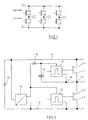
- the drive circuit 10 receives its power supply from a capacitor 16 connected to the power supply via a diode 18 14 lies.
- the reference potential of the drive circuit 10, as shown at 18, is at the same potential as a connection point 20 between the Source of the high-side transistor and the drain of the low-side transistor and with it a phase.
- the reference potential for the control circuit 10 is the minus potential the battery designated 22, which the three-phase motor with energy provided.
- the transistors are switched alternately by the control circuits 10, 12. As a result, the potential of points 18 and 20 jumps back and forth between positive and negative power supply.
- the capacitor 16 can only be charged when the low-side transistor is on and the high-side transistor is off.
- the current from the power supply 14 can then charge the capacitor 16 via the diode 18. If the high-side transistor is on and the low-side transistor is off, that is Jumping reference potential "18 at the potential of the positive current supply. Now the control circuit 10 can only be supplied from the capacitor 16, because the diode 18 is in the off state is pumped ".
- the reference potential jumps (jumping potential) back and forth, so that the reference potential and the measuring inputs for the measuring amplifier 28 jump.
- the reference potential jumps (jumping potential) back and forth, so that the reference potential and the measuring inputs for the measuring amplifier 28 jump.
- special circuit measures is a control and supply of the measuring amplifier 28 with a fixed Reference potential not possible.
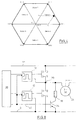
- FIG. 4 shows the space vector diagram of a space vector modulation.
- the Control of the high-side transistor is with the number 1 and that of the low-side transistor marked with the number 0.
- the state of the converter with its three phases can then be specified as a triple, e.g. B. 0 0 1. Since the three phases are one Three-phase on a circle shifted by 120 ° spatially shown as a pointer can be obtained for the individual switching states of the converter 1 six vectors, which are also referred to as base vectors and create a regular hexagon. Two states, namely control of all High-side or low-side transistors (1 1 1 or 0 0 0) are called zero vectors designated. There are six sectors between the base vectors, which correspond in FIG. 4 are designated.
- FIGS. 4 and 7 in an odd sector, the base vectors clockwise, in laid out in a straight counter-clockwise direction. This ensures that the zero vector is only generated by switching on all low-side transistors. This can be clearly seen from FIG. 7. 10 shows the voltage curve of phase 1 9, but in the method according to the invention.
- FIG. 8 contains the same components as Fig. 2 and 3, it is therefore provided with the same reference numerals.
- An auxiliary transistor 34 which lies between connection point 20 and negative potential and one Resistor 36 is connected in series is from an electronic control unit 38 for the Control circuits 10 and 12 for the half-bridge shown also with a blocking signal acted on via a line 40 when the inverter is locked.
- the auxiliary transistor 34 is driven by the blocking signal and turns on at point 20 Potential generated, for example on half of the positive power supply V + lies. This potential serves as a reference potential for the control circuit 10 or the Measuring amplifier, not shown in Fig. 8 (see position 28 of Fig. 3).
- the Fig. 8 circuit arrangement causes that after cancellation of the lock signal the storage capacitors of the charge pumps (see FIG. 3) are charged.
- auxiliary transistor 34 is connected to only one motor phase.
- the other motor phases due to the corresponding winding phases of the motor Connection.
- the resistor 36 has the task of switching the current at a moment's notice to limit.
Landscapes
- Engineering & Computer Science (AREA)
- Power Engineering (AREA)
- Inverter Devices (AREA)
- Control Of Ac Motors In General (AREA)
Abstract
Description

- Fig. 1
- zeigt einen Wechselstrom-Umrichter mit drei Halbbrücken.
- Fig. 2
- zeigt eine Halbbrücke nach Fig. 1 mit dem Prinzipschaltbild einer Ladungspumpe.
- Fig. 3
- zeigt eine Halbbrücke nach Fig. 1 mit Ladungspumpe und einem Strommeßverstärker.
- Fig. 4
- zeigt ein Raumzeigerdiagramm einer Raumzeigermodulation für einen Umformer nach Fig. 1.
- Fig. 5
- zeigt ein Diagramm für die Raumzeigermodulation im Sektor 1 nach Fig. 4.
- Fig. 6
- zeigt eine Raumzeigermodulation in Sektor 2 nach Fig. 4.
- Fig. 7
- zeigt eine erfindungsgemäße Modulation in Sektor 1 nach Fig. 4.
- Fig. 8
- zeigt ein ähnliches Schaltbild wie Fig. 1, jedoch mit einem zusätzlichen Schaltungsteil.
- Fig. 9
- zeigt das Diagramm einer gefilterten Ausgangsspannung einer Phase des Umrichters nach Fig. 1 mit einer Raumzeigermodulation nach Fig. 5 und 6.
- Fig. 10
- zeigt die gefilterte Ausgangsspannung einer Phase nach der erfindungsgemäßen Modulation.
Claims (2)
- Verfahren zum Betrieb eines Drehstromumrichters, der in drei Halbbrücken jeweils mindestens zwei Leistungstransistoren aufweist zur Erzeugung eines Drehstroms aus Gleichstrom für Drehstrommotoren, insbesondere in Flurförderzeugen, bei dem zur Erzeugung beliebiger Spannungswerte die Leistungstransistoren nach der Raumzeigermodulation mit hoher Trägerfrequenz nach Art der symmetrischen Pulsweitenmodulation (PWM) innerhalb der Trägerperiodendauer zwischen zwei benachbarten Basisvektoren und einem Nullvektor eines Sektors umgeschaltet werden, dadurch gekennzeichnet, daß in den ungeradzahligen Sektoren die Basisvektoren in einer ersten Drehrichtung und in den geradzahligen Sektoren in der entgegengesetzten Drehrichtung angelegt werden derart, daß der Nullvektor nur durch Einschalten der am Minuspotential liegenden Transistoren erzeugt wird.
- Verfahren nach Anspruch 1, bei dem die Spannungsversorgung der Ansteuerelektronik der Transistoren und ggf. eines mit einem Shunt in einer Phase verbundenen Meßverstärkers mit Hilfe einer einen Kondensator und eine Diode enthaltenden Ladungspumpe erfolgt, dadurch gekennzeichnet, daß mit Hilfe des Sperrsignals für alle Transistoren ein Hilfstransistor angesteuert wird, der einen Verbindungspunkt zwischen den Transistoren einer Halbbrücke mit dem Minuspotential über einen Begrenzungswiderstand verbindet.
Applications Claiming Priority (2)
| Application Number | Priority Date | Filing Date | Title |
|---|---|---|---|
| DE19910327 | 1999-03-09 | ||
| DE1999110327 DE19910327C2 (de) | 1999-03-09 | 1999-03-09 | Verfahren zum Betrieb eines Drehstromumrichters für Drehstrommotoren |
Publications (3)
| Publication Number | Publication Date |
|---|---|
| EP1035642A1 true EP1035642A1 (de) | 2000-09-13 |
| EP1035642B1 EP1035642B1 (de) | 2007-06-20 |
| EP1035642B2 EP1035642B2 (de) | 2013-03-27 |
Family
ID=7900241
Family Applications (1)
| Application Number | Title | Priority Date | Filing Date |
|---|---|---|---|
| EP00100094A Expired - Lifetime EP1035642B2 (de) | 1999-03-09 | 2000-01-07 | Pulsweitenmodulation zum Betrieb eines Drehstromumrichters für Drehstrommotoren |
Country Status (2)
| Country | Link |
|---|---|
| EP (1) | EP1035642B2 (de) |
| DE (2) | DE19910327C2 (de) |
Cited By (3)
| Publication number | Priority date | Publication date | Assignee | Title |
|---|---|---|---|---|
| EP1225452A3 (de) * | 2001-01-19 | 2004-01-28 | Robert Bosch Gmbh | Verfahren zur Messung des Stromes in Halbbrücken |
| DE102006042384B4 (de) * | 2006-09-08 | 2008-09-11 | Siemens Ag | Umrichter und Verfahren zur Steuerung eines Umrichters |
| EP2028756A1 (de) * | 2007-08-23 | 2009-02-25 | Siemens Aktiengesellschaft | Umrichter mit Kurzschlussschutz |
Families Citing this family (5)
| Publication number | Priority date | Publication date | Assignee | Title |
|---|---|---|---|---|
| DE102009045052B4 (de) | 2008-09-30 | 2013-04-04 | Infineon Technologies Ag | Bereitstellen einer Versorgungsspannung für eine Ansteuerschaltung eines Halbleiterschaltelements |
| DE102008049677B4 (de) | 2008-09-30 | 2014-09-18 | Infineon Technologies Ag | Spannungsversorgung in einer Schaltungsanordnung mit einem Halbleiterschaltelement |
| DE102008049673B4 (de) | 2008-09-30 | 2011-04-28 | Infineon Technologies Ag | Schaltungsanordnung mit einem Leistungshalbleitermodul und einer außerhalb dessen angeordneten Steuerschaltung |
| DE102016112815A1 (de) | 2016-07-13 | 2018-01-18 | Jungheinrich Aktiengesellschaft | Steuerung eines Drehstrommotors mit einem Kennlinienfeld sowie Verfahren zur Bestimmung desselben |
| DE102024120649A1 (de) * | 2024-07-19 | 2026-01-22 | Jungheinrich Aktiengesellschaft | Verfahren zum Betreiben einer mindestens dreiphasigen Induktionsmaschine und Induktionsmaschine |
Family Cites Families (2)
| Publication number | Priority date | Publication date | Assignee | Title |
|---|---|---|---|---|
| JP2634306B2 (ja) * | 1990-08-08 | 1997-07-23 | 三菱電機株式会社 | インバータ装置の駆動回路 |
| DK172570B1 (da) * | 1995-01-23 | 1999-01-25 | Danfoss As | Vekselretter og fremgangsmåde til måling af vekselretterens fasestrømme |
-
1999
- 1999-03-09 DE DE1999110327 patent/DE19910327C2/de not_active Expired - Lifetime
-
2000
- 2000-01-07 DE DE50014420T patent/DE50014420D1/de not_active Expired - Lifetime
- 2000-01-07 EP EP00100094A patent/EP1035642B2/de not_active Expired - Lifetime
Non-Patent Citations (2)
| Title |
|---|
| HANDLEY P G, BOYS J T: "Space vector modulation: an engineering review", July 1990, FOURTH INTERNATIONAL CONFERENCE ON POWER ELECTRONICS AND VARIABLE-SPEED DRIVES, UK, LONDON, XP002139656 * |
| HOLMES D G: "THE GENERAL RELATIONSHIP BETWEEN REGULAR-SAMPLED PULSE-WIDTH- MODULATION AND SPACE VECTOR MODULATION FOR HARD SWITCHED CONVERTERS", 9 October 1992, PROCEEDINGS OF THE INDUSTRY APPLICATIONS SOCIETY ANNUAL MEETING,US,NEW YORK, IEEE, VOL. -, PAGE(S) 1002-1009, ISBN: 0-7803-0635-X, XP000368904 * |
Cited By (6)
| Publication number | Priority date | Publication date | Assignee | Title |
|---|---|---|---|---|
| EP1225452A3 (de) * | 2001-01-19 | 2004-01-28 | Robert Bosch Gmbh | Verfahren zur Messung des Stromes in Halbbrücken |
| DE102006042384B4 (de) * | 2006-09-08 | 2008-09-11 | Siemens Ag | Umrichter und Verfahren zur Steuerung eines Umrichters |
| US7948779B2 (en) | 2006-09-08 | 2011-05-24 | Siemens Aktiengesellschaft | Converter with reduced harmonic waves |
| EP2028756A1 (de) * | 2007-08-23 | 2009-02-25 | Siemens Aktiengesellschaft | Umrichter mit Kurzschlussschutz |
| WO2009024391A1 (en) * | 2007-08-23 | 2009-02-26 | Siemens Ag | An inverter with short circuit protection |
| US8681516B2 (en) | 2007-08-23 | 2014-03-25 | Siemens Aktiengesellschaft | Inverter with short circuit protection |
Also Published As
| Publication number | Publication date |
|---|---|
| DE19910327C2 (de) | 2001-11-22 |
| EP1035642B2 (de) | 2013-03-27 |
| DE19910327A1 (de) | 2000-09-21 |
| EP1035642B1 (de) | 2007-06-20 |
| DE50014420D1 (de) | 2007-08-02 |
Similar Documents
| Publication | Publication Date | Title |
|---|---|---|
| DE3105094C2 (de) | Pulsbreitenmodulations-Wechselrichtervorrichtung | |
| DE112017003632T5 (de) | Dc/dc-umrichter | |
| DE10156939A1 (de) | Schaltungsanordnung zum Betreiben einer elektrischenMaschine | |
| DE19910327C2 (de) | Verfahren zum Betrieb eines Drehstromumrichters für Drehstrommotoren | |
| DE202019005419U1 (de) | Steuerung für elektrische Servolenkungsteuerung für elektrische Servolenkung | |
| EP2945288A1 (de) | Schaltungsanordnung und verfahren zum ansteuern eines halbleiterschaltelements | |
| WO2014206696A1 (de) | Z-source wechselrichter mit optimiertem wirkungsgrad | |
| EP0891037B1 (de) | Pulsweitenmodulationsverfahren für in Serie geschaltete Umrichter | |
| WO2023083406A1 (de) | Wechselrichtersystem und verfahren zu dessen betrieb | |
| DE112023001779T5 (de) | Linearmotor-Antriebseinrichtung und Linearmotor | |
| EP0366892A2 (de) | Schaltungsanordnung zur Ansteuerung eines bürstenlosen Gleichstrommotors | |
| EP4183039A1 (de) | Statormodul für ein lineares transportsystem | |
| EP2544350B1 (de) | Kommutierungsschaltung, elektrischer Energiewandler und Kommutierungsverfahren | |
| EP2375551B1 (de) | Kommutierungsverfahren, Kommutierungsschaltung und elektrischer Energiewandler | |
| EP0744820B1 (de) | Schaltungsanordnung zum Speisen einer Last | |
| EP0581091B1 (de) | Vorschaltgerät zum Betreiben von Hockdruck-Gasentladungslampen mit niederfrequenter, rechteckförmiger Spannung in Kraftfahrzeugen | |
| EP3834279A1 (de) | Raumzeigermodulationsverfahren mit berücksichtigung von mindestschaltzustandszeiten zum steueren einer mehrphasigen elektrische maschine | |
| DE102005028605B4 (de) | Verfahren zur Strommessung mit einem Shunt und Vorrichtung zur Strommessung | |
| EP1768253A2 (de) | Verfahren zur Strommessung mit einem Shunt und Vorrichtung zur Strommessung | |
| DE102023115495A1 (de) | Verfahren und Vorrichtung zur Ermittlung eines Schaltmusters für den Betrieb eines Wechselrichters | |
| WO2024032998A1 (de) | Verfahren zum ausgleichen einer mittelpunktspannung eines 3-level-inverters | |
| EP1398877B1 (de) | Verfahren zur Fehlererkennung in der Datenübertragung zu einer Treiberschaltung | |
| DE102016204182A1 (de) | Schaltungsanordnung und Verfahren zur integrierten Gate-Spannungsversorgung eines High-Side-Halbleiters in einem Wechselrichter | |
| DE102022132875A1 (de) | Verfahren zur Ansteuerung eines Stromrichters | |
| DE102023114712A1 (de) | Verfahren und Vorrichtung zum Betreiben eines mehrstufigen Wechselrichters |
Legal Events
| Date | Code | Title | Description |
|---|---|---|---|
| PUAI | Public reference made under article 153(3) epc to a published international application that has entered the european phase |
Free format text: ORIGINAL CODE: 0009012 |
|
| AK | Designated contracting states |
Kind code of ref document: A1 Designated state(s): DE FR GB IT SE |
|
| AX | Request for extension of the european patent |
Free format text: AL;LT;LV;MK;RO;SI |
|
| 17P | Request for examination filed |
Effective date: 20010112 |
|
| AKX | Designation fees paid |
Free format text: DE FR GB IT SE |
|
| GRAP | Despatch of communication of intention to grant a patent |
Free format text: ORIGINAL CODE: EPIDOSNIGR1 |
|
| GRAS | Grant fee paid |
Free format text: ORIGINAL CODE: EPIDOSNIGR3 |
|
| GRAA | (expected) grant |
Free format text: ORIGINAL CODE: 0009210 |
|
| AK | Designated contracting states |
Kind code of ref document: B1 Designated state(s): DE FR GB IT SE |
|
| REG | Reference to a national code |
Ref country code: GB Ref legal event code: FG4D Free format text: NOT ENGLISH |
|
| REF | Corresponds to: |
Ref document number: 50014420 Country of ref document: DE Date of ref document: 20070802 Kind code of ref document: P |
|
| GBT | Gb: translation of ep patent filed (gb section 77(6)(a)/1977) |
Effective date: 20070903 |
|
| REG | Reference to a national code |
Ref country code: SE Ref legal event code: TRGR |
|
| ET | Fr: translation filed | ||
| PLBI | Opposition filed |
Free format text: ORIGINAL CODE: 0009260 |
|
| PLAX | Notice of opposition and request to file observation + time limit sent |
Free format text: ORIGINAL CODE: EPIDOSNOBS2 |
|
| 26 | Opposition filed |
Opponent name: DIEHL AKO STIFTUNG & CO. KG Effective date: 20080320 |
|
| PLAF | Information modified related to communication of a notice of opposition and request to file observations + time limit |
Free format text: ORIGINAL CODE: EPIDOSCOBS2 |
|
| PLBB | Reply of patent proprietor to notice(s) of opposition received |
Free format text: ORIGINAL CODE: EPIDOSNOBS3 |
|
| PLAB | Opposition data, opponent's data or that of the opponent's representative modified |
Free format text: ORIGINAL CODE: 0009299OPPO |
|
| R26 | Opposition filed (corrected) |
Opponent name: DIEHL AKO STIFTUNG & CO. KG Effective date: 20080320 |
|
| PGFP | Annual fee paid to national office [announced via postgrant information from national office to epo] |
Ref country code: FR Payment date: 20120201 Year of fee payment: 13 |
|
| PGFP | Annual fee paid to national office [announced via postgrant information from national office to epo] |
Ref country code: SE Payment date: 20120124 Year of fee payment: 13 Ref country code: GB Payment date: 20120124 Year of fee payment: 13 Ref country code: IT Payment date: 20120125 Year of fee payment: 13 |
|
| PUAH | Patent maintained in amended form |
Free format text: ORIGINAL CODE: 0009272 |
|
| STAA | Information on the status of an ep patent application or granted ep patent |
Free format text: STATUS: PATENT MAINTAINED AS AMENDED |
|
| 27A | Patent maintained in amended form |
Effective date: 20130327 |
|
| AK | Designated contracting states |
Kind code of ref document: B2 Designated state(s): DE FR GB IT SE |
|
| REG | Reference to a national code |
Ref country code: DE Ref legal event code: R102 Ref document number: 50014420 Country of ref document: DE Effective date: 20130327 |
|
| REG | Reference to a national code |
Ref country code: SE Ref legal event code: NAV |
|
| GBPC | Gb: european patent ceased through non-payment of renewal fee |
Effective date: 20130107 |
|
| REG | Reference to a national code |
Ref country code: FR Ref legal event code: ST Effective date: 20130930 |
|
| PG25 | Lapsed in a contracting state [announced via postgrant information from national office to epo] |
Ref country code: FR Free format text: LAPSE BECAUSE OF NON-PAYMENT OF DUE FEES Effective date: 20130131 Ref country code: GB Free format text: LAPSE BECAUSE OF NON-PAYMENT OF DUE FEES Effective date: 20130107 |
|
| PG25 | Lapsed in a contracting state [announced via postgrant information from national office to epo] |
Ref country code: IT Free format text: LAPSE BECAUSE OF NON-PAYMENT OF DUE FEES Effective date: 20130107 |
|
| PG25 | Lapsed in a contracting state [announced via postgrant information from national office to epo] |
Ref country code: SE Free format text: LAPSE BECAUSE OF NON-PAYMENT OF DUE FEES Effective date: 20130108 |
|
| PGFP | Annual fee paid to national office [announced via postgrant information from national office to epo] |
Ref country code: DE Payment date: 20180329 Year of fee payment: 19 |
|
| REG | Reference to a national code |
Ref country code: DE Ref legal event code: R119 Ref document number: 50014420 Country of ref document: DE |
|
| PG25 | Lapsed in a contracting state [announced via postgrant information from national office to epo] |
Ref country code: DE Free format text: LAPSE BECAUSE OF NON-PAYMENT OF DUE FEES Effective date: 20190801 |