EP1035564A2 - Diffusion barrier for high dielectric constant materials - Google Patents
Diffusion barrier for high dielectric constant materials Download PDFInfo
- Publication number
- EP1035564A2 EP1035564A2 EP00300158A EP00300158A EP1035564A2 EP 1035564 A2 EP1035564 A2 EP 1035564A2 EP 00300158 A EP00300158 A EP 00300158A EP 00300158 A EP00300158 A EP 00300158A EP 1035564 A2 EP1035564 A2 EP 1035564A2
- Authority
- EP
- European Patent Office
- Prior art keywords
- metal
- layer
- electronic device
- diffusion barrier
- nitride
- Prior art date
- Legal status (The legal status is an assumption and is not a legal conclusion. Google has not performed a legal analysis and makes no representation as to the accuracy of the status listed.)
- Withdrawn
Links
Images

Classifications
-
- H—ELECTRICITY
- H10—SEMICONDUCTOR DEVICES; ELECTRIC SOLID-STATE DEVICES NOT OTHERWISE PROVIDED FOR
- H10D—INORGANIC ELECTRIC SEMICONDUCTOR DEVICES
- H10D1/00—Resistors, capacitors or inductors
- H10D1/60—Capacitors
- H10D1/68—Capacitors having no potential barriers
-
- H—ELECTRICITY
- H10—SEMICONDUCTOR DEVICES; ELECTRIC SOLID-STATE DEVICES NOT OTHERWISE PROVIDED FOR
- H10P—GENERIC PROCESSES OR APPARATUS FOR THE MANUFACTURE OR TREATMENT OF DEVICES COVERED BY CLASS H10
- H10P14/00—Formation of materials, e.g. in the shape of layers or pillars
- H10P14/40—Formation of materials, e.g. in the shape of layers or pillars of conductive or resistive materials
- H10P14/418—Formation of materials, e.g. in the shape of layers or pillars of conductive or resistive materials the conductive layers comprising transition metals
Definitions
- the present invention relates to diffusion barriers, and more particularly, to improved diffusion barriers for use with high dielectric constant materials.
- DRAMs dynamic random access memories
- RF radio frequency
- MOM metal-oxide-metal
- MOS metal-oxide-silicon
- tantalum pentoxide (Ta 2 O 5 ) has been proposed as an alternative to SiO 2 with the advantage that it can be deposited by a law-temperature process ( ⁇ 500°C).
- TiN titanium nitride
- a MOM capacitor could be formed from a layered stack of Al/TiN/Ta 2 O 5 /TiN/Ti.
- a gate structure for an MOS transistor could be formed from a layered stack of Al/TiN/ Ta 2 O 5 /SiO2/Si. It should be understood that many variations of the foregoing MOM capacitor and MOS transistor structures are well known in the art and the foregoing structures are meant to be illustrative and not limiting.
- Ta 2 O 5 /TiN structures One problem associated with Ta 2 O 5 /TiN structures is that oxygen tends to migrate from the otherwise stable Ta 2 O 5 and diffuse into the TiN during heat treatments, especially in cases where the TiN is Ti-rich. In the case of Ta 2 O 5 /TiN/Ti structures, such as in a MOM capacitor, the oxygen diffuses into the Ti. This diffusion of oxygen tends to reduce the Ta 2 O 5 to elemental metal Ta. It has been found that this oxygen diffusion and reduction of Ta 2 O 5 can occur at temperatures as low as 400-600°C. This can be a serious problem when manufacturing electronic devices incorporating Ta 2 O 5 /TiN and Ta 2 O 5 /TiN/Ti structures as the resulting devices will have high leakage currents or will otherwise be inadequate or, in extreme cases, inoperable.
- the present invention is directed to a diffusion barrier that substantially obviates one or more of the problems due to limitations and disadvantages of the related art.
- the invention provides an electronic device comprising a titanium nitride layer, a high dielectric constant material, and a diffusion barrier disposed between the titanium nitride layer and the high dielectric constant material to prevent the diffusion of oxygen from the high dielectric constant material to the titanium nitride layer.
- the invention also provides a metal-oxide-metal capacitor comprising a first interconnect layer, a first titanium nitride layer adjacent to the first interconnect layer, a first diffusion barrier adjacent to the first titanium nitride layer, a tantalum pentoxide layer adjacent to the first diffusion barrier, a second diffusion barrier adjacent to the tantalum pentoxide layer, a second titanium nitride layer adjacent to the second diffusion barrier, and a second interconnect layer adjacent to the second titanium nitride layer, wherein the first diffusion barrier prevents the diffusion of oxygen from the tantalum pentoxide layer into the first titanium nitride layer and the first titanium layer, and wherein the second diffusion barrier prevents the diffusion of oxygen from the tantalum pentoxide layer into the second titanium nitride layer.
- the invention also provides a metal-oxide-semiconductor transistor having a gate structure, the gate structure comprising an interconnect layer, a titanium nitride layer adjacent to the interconnect layer, a diffusion barrier adjacent to the titanium nitride layer, a tantalum pentoxide layer adjacent to the diffusion barrier, and a gate insulator adjacent to the tantalum pentoxide layer, wherein the diffusion barrier prevents the diffusion of oxygen from the tantalum pentoxide layer into the titanium nitride layer.
- the invention also provides a diffusion barrier for preventing the diffusion of oxygen from a high dielectric constant material to a titanium nitride layer, the diffusion barrier comprising one or more layers, wherein each of the one or more layers comprises a material selected from the group consisting of metal carbide, metal nitride, metal boride, metal carbo-nitride, and silicon carbide.
- a diffusion barrier for use with a Ta 2 O 5 /TiN structure according to the present invention is shown in Fig. 1 and is designated generally by reference numeral 100.
- the diffusion barrier 100 is disposed between a Ta 2 O 5 layer 105 and a TiN layer 110 to prevent the diffusion of oxygen from the Ta 2 O 5 layer 105 to the TiN layer 110 and, therefore, prevent the reduction of the Ta 2 O 5 layer 105 to elemental metal Ta.
- the diffusion barrier 100 comprises one or more layers (in any combination), wherein each of the one or more layers comprises one of the following materials: metal carbide, metal nitride, metal boride, metal carbo-nitride, and silicon carbide.
- the diffusion barrier 100 can comprise a single layer of metal carbide, a single layer of metal nitride, a single layer of metal boride, a single layer of metal carbo-nitride, or a single layer of silicon carbide.
- the diffusion barrier 100 can comprise two or more layers (in any combination), wherein each of the two or more layers is a single layer of metal carbide, a single layer of metal nitride, a single layer of metal boride, a single layer of metal carbo-nitride, or a single layer of silicon carbide.
- the metal carbide can be any metal carbide, including but not limited to titanium carbide, tantalum carbide, zirconium carbide, molybdenum carbide, tungsten carbide, and chromium carbide.
- the metal nitride can be any metal nitride, including but not limited to aluminum nitride, tungsten nitride, molybdenum nitride, zirconium nitride, and vanadium nitride.
- the metal boride can be any metal boride, including but not limited to titanium boride and zirconium boride.
- any refractory metal can be used as the metal in each of the metal carbide, metal nitride, and metal boride.
- each layer of the diffusion barrier 100 has a thickness of about 10-50 ⁇ .
- a thickness of about 10-200 ⁇ , 50-1000 ⁇ or 200-300 ⁇ is also acceptable.
- the diffusion barrier 100 can he formed by any technique known to those skilled in the art, include physical and/or chemical vapor deposition.
- deposition of the diffusion barrier materials is preferably performed in a nitrogen-containing atmosphere.
- deposition can be performed using tungsten carbonyl or tungsten hexoflouride as a precursor material.
- metal carbide, metal nitride, metal boride, metal carbo-nitride, and/or silicon carbide as the diffusion barrier 100 material(s) has certain advantages over the use of other materials in terms of both the quality of the interfaces between the materials and the adjacent TiN layer 110 and, in the case of a multi-layer diffusion barrier 100, the quality of the interfaces between each of the layers that make up the diffusion barrier 100.
- metal carbide, metal nitride, and metal boride each has a cubic structure and therefore provides a low lattice misfit interface with the TiN layer 110, which also has a cubic structure (i.e., the diffusion barrier/TiN interface is substantially coherent).
- the interface(s) between the multiple layers are also substantially coherent, again because each of the layers has a cubic structure.
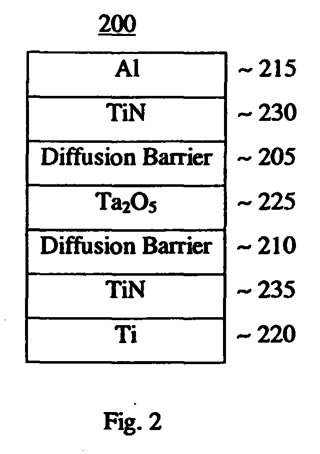
- Fig. 2 illustrates an example of a MOM capacitor 200 including the diffusion barrier according to the present invention.
- the MOM capacitor comprises a layered stack of Al/TiN/diffusion barrier/Ta 2 O 5 /diffusion barrier/TiN/Ti.
- the diffusion barrier 205 prevents the diffusion of oxygen from the Ta 2 O 5 layer 225 into the TiN layer 230
- the diffusion barrier 210 prevents the diffusion of oxygen from the Ta 2 O 5 layer 225 into the TiN layer 235 and the Ti layer 220.
- the diffusion barriers 205 and 210 can have any of the configurations described above with regard to the diffusion barrier 100. Further, the diffusion barriers 205 and 210 need not have the same configurations.
- the Ti layer 220 and the Al layer 215, which serve as interconnect layers, can be replaced with other materials known to those skilled in the art for performing their respective functions.
- the Ti layer 220 can be replaced with a tantalum or tantalum nitride layer
- the Al layer 215 can be replaced with a copper layer.
- Fig. 3 illustrates an example of an MOS transistor gate structure 300 including the diffusion barrier according to the present invention.
- the gate structure 300 comprises a layered stack (provided on a silicon substrate 305) of SiO 2 /Ta 2 O 5 /diffusion barrier/TiN/Al.
- the diffusion barrier 310 prevents the diffusion of oxygen from the Ta 2 O 5 layer 315 into the TiN layer 320.
- the diffusion barrier 310 can have any of the configurations described above with regard to the diffusion barrier 100.
- the SiO 2 layer 325 and the Al layer 330 which serve as a gate insulator and interconnect layer, respectively, can be replaced with other materials known to those skilled in the art for performing their respective functions.
- the SiO 2 layer 325 can be replaced by a Ta 2 O 5 layer or a combination of a Ta 2 O 5 layer and an SiO 2 layer.
- the Ta 2 O 5 layer 315 itself can serve as the gate insulator in which case the SiO 2 layer 325 would not be present.
- the diffusion barrier according to the present invention has been described for use with a Ta 2 O 5 /TiN structure, it is also useful as a diffusion barrier for a Ta2O5/TiN/Ti structure, as well as an X/TiN structure and an X/TiN/Ti structure, where X is any perkovskite-type high dielectric constant material, including but not limited to barium-based oxides, strontium-based oxides, lanthanum-based oxides, zirconium-based oxides, titanates of each of the foregoing oxides, and a combination of two or more of the foregoing.
- X any perkovskite-type high dielectric constant material
Landscapes
- Semiconductor Memories (AREA)
- Semiconductor Integrated Circuits (AREA)
- Insulated Gate Type Field-Effect Transistor (AREA)
- Electrodes Of Semiconductors (AREA)
Abstract
A diffusion barrier for preventing the diffusion of oxygen from a high dielectric
constant material to a titanium nitride layer. The diffusion barrier comprises one or
more layers, wherein each of the one or more layers comprises a material selected from
the group consisting of metal carbide, metal nitride, metal boride, metal carbo-nitride,
and silicon carbide. The high dielectric constant material may be tantalum pentoxide or
any perkovskite-type high dielectric constant material.
Description
- The present invention relates to diffusion barriers, and more particularly, to improved diffusion barriers for use with high dielectric constant materials.
- High dielectric constant materials (εr » εSiO2 = 3.9 ε0) have been widely studied as a replacement for silicon dioxide (SiO2) and silicon nitride (Si3N4) in silicon-based electronic devices, such as capacitors in dynamic random access memories (DRAMs), radio frequency (RF) circuits, metal-oxide-metal (MOM) capacitors, and metal-oxide-silicon (MOS) transistors. (See, e.g., P.K. Roy and I.C. Kizilyalli, "Stacked High-ε Gate Dielectric for Gigascale Integration of Metal-Oxide-Semiconductor Technologies," Applied Physics Letters, Vol. 72, No. 22, pp. 2835-2837 (June 1, 1988), and I.C. Kizilyalli, et al., "MOS Transistors with Stacked SiO2-Ta2O5-SiO2 Gate Dielectrics for Giga-Scale Integration of CMOS Technologies," IEEE Electron Device Letters, Vol. 19, No. 11, pp. 423-425 (Nov. 1998), both of which are incorporated by reference herein).
- In particular, tantalum pentoxide (Ta2O5) has been proposed as an alternative to SiO2 with the advantage that it can be deposited by a law-temperature process (<500°C). Generally, when manufacturing electronic devices incorporating Ta2O5, it may be advantageous to provide a titanium nitride (TiN) layer adjacent to the Ta2O5, for example, as a diffusion barrier or electrode, to form a Ta2O5/TiN structure. For example, a MOM capacitor could be formed from a layered stack of Al/TiN/Ta2O5/TiN/Ti. Likewise, a gate structure for an MOS transistor could be formed from a layered stack of Al/TiN/ Ta2O5/SiO2/Si. It should be understood that many variations of the foregoing MOM capacitor and MOS transistor structures are well known in the art and the foregoing structures are meant to be illustrative and not limiting.
- One problem associated with Ta2O5/TiN structures is that oxygen tends to migrate from the otherwise stable Ta2O5 and diffuse into the TiN during heat treatments, especially in cases where the TiN is Ti-rich, In the case of Ta2O5/TiN/Ti structures, such as in a MOM capacitor, the oxygen diffuses into the Ti. This diffusion of oxygen tends to reduce the Ta2O5 to elemental metal Ta. It has been found that this oxygen diffusion and reduction of Ta2O5 can occur at temperatures as low as 400-600°C. This can be a serious problem when manufacturing electronic devices incorporating Ta2O5/TiN and Ta2O5/TiN/Ti structures as the resulting devices will have high leakage currents or will otherwise be inadequate or, in extreme cases, inoperable.
- Accordingly, the present invention is directed to a diffusion barrier that substantially obviates one or more of the problems due to limitations and disadvantages of the related art.
- Additional features and advantages of the invention will be set forth in the description that follows and, in part, will be apparent from the description, or may be learned by practice of the invention. The objectives and other advantages of the invention will be realized and attained by the diffusion barrier and method particularly pointed out in the written description and claims hereof as well as the appended drawings.
- To achieve these and other advantages and in accordance with the purposes of the invention, as embodied and broadly described, the invention provides an electronic device comprising a titanium nitride layer, a high dielectric constant material, and a diffusion barrier disposed between the titanium nitride layer and the high dielectric constant material to prevent the diffusion of oxygen from the high dielectric constant material to the titanium nitride layer.
- To further achieve these and other advantages and in accordance with the purposes of the invention, as embodied and broadly described, the invention also provides a metal-oxide-metal capacitor comprising a first interconnect layer, a first titanium nitride layer adjacent to the first interconnect layer, a first diffusion barrier adjacent to the first titanium nitride layer, a tantalum pentoxide layer adjacent to the first diffusion barrier, a second diffusion barrier adjacent to the tantalum pentoxide layer, a second titanium nitride layer adjacent to the second diffusion barrier, and a second interconnect layer adjacent to the second titanium nitride layer, wherein the first diffusion barrier prevents the diffusion of oxygen from the tantalum pentoxide layer into the first titanium nitride layer and the first titanium layer, and wherein the second diffusion barrier prevents the diffusion of oxygen from the tantalum pentoxide layer into the second titanium nitride layer.
- To still further achieve these and other advantages and in accordance with the purposes of the invention, as embodied and broadly described, the invention also provides a metal-oxide-semiconductor transistor having a gate structure, the gate structure comprising an interconnect layer, a titanium nitride layer adjacent to the interconnect layer, a diffusion barrier adjacent to the titanium nitride layer, a tantalum pentoxide layer adjacent to the diffusion barrier, and a gate insulator adjacent to the tantalum pentoxide layer, wherein the diffusion barrier prevents the diffusion of oxygen from the tantalum pentoxide layer into the titanium nitride layer.
- To still even further achieve these and other advantages and in accordance with the purposes of the invention, as embodied and broadly described, the invention also provides a diffusion barrier for preventing the diffusion of oxygen from a high dielectric constant material to a titanium nitride layer, the diffusion barrier comprising one or more layers, wherein each of the one or more layers comprises a material selected from the group consisting of metal carbide, metal nitride, metal boride, metal carbo-nitride, and silicon carbide.
- It is to be understood that both the foregoing general description and the following detailed description are exemplary and explanatory and are intended to provide further explanation of the invention as claimed.
- The accompanying drawings, which are included to provide a further understanding of the invention and are incorporated in and constitute a part of this specification, illustrate several embodiments of the invention and, together with the written description, serve to explain the principles of the invention. In the drawings:
- Fig. 1 is a cross-sectional view of a Ta2O5/diffusion barrier/TiN structure according to the present invention;
- Fig. 2 is a cross-sectional view of an MOM capacitor according to the present invention; and
- Fig. 3 is a cross-sectional view of an MOS transistor gate structure according to the present invention.
-
- Reference will now be made in detail to the presently preferred embodiments of the invention, examples of which is illustrated in the accompanying drawings.
- A diffusion barrier for use with a Ta2O5/TiN structure according to the present invention is shown in Fig. 1 and is designated generally by
reference numeral 100. As embodied herein, thediffusion barrier 100 is disposed between a Ta2O5 layer 105 and aTiN layer 110 to prevent the diffusion of oxygen from the Ta2O5 layer 105 to theTiN layer 110 and, therefore, prevent the reduction of the Ta2O5 layer 105 to elemental metal Ta. In a preferred embodiment, thediffusion barrier 100 comprises one or more layers (in any combination), wherein each of the one or more layers comprises one of the following materials: metal carbide, metal nitride, metal boride, metal carbo-nitride, and silicon carbide. Thus, for example, thediffusion barrier 100 can comprise a single layer of metal carbide, a single layer of metal nitride, a single layer of metal boride, a single layer of metal carbo-nitride, or a single layer of silicon carbide. Alternatively, thediffusion barrier 100 can comprise two or more layers (in any combination), wherein each of the two or more layers is a single layer of metal carbide, a single layer of metal nitride, a single layer of metal boride, a single layer of metal carbo-nitride, or a single layer of silicon carbide. - It should be understand that the metal carbide can be any metal carbide, including but not limited to titanium carbide, tantalum carbide, zirconium carbide, molybdenum carbide, tungsten carbide, and chromium carbide. Further, it should be understood that the metal nitride can be any metal nitride, including but not limited to aluminum nitride, tungsten nitride, molybdenum nitride, zirconium nitride, and vanadium nitride. Still further, it should be understood that the metal boride can be any metal boride, including but not limited to titanium boride and zirconium boride. Preferably, any refractory metal can be used as the metal in each of the metal carbide, metal nitride, and metal boride.
- Preferably, each layer of the
diffusion barrier 100 has a thickness of about 10-50Å. However, A thickness of about 10-200Å, 50-1000Å or 200-300Å is also acceptable. Further, thediffusion barrier 100 can he formed by any technique known to those skilled in the art, include physical and/or chemical vapor deposition. For example, in the case of sputtering nitrides, deposition of the diffusion barrier materials is preferably performed in a nitrogen-containing atmosphere. As another example, in the case of depositing tungsten nitride by chemical vapor deposition, deposition can be performed using tungsten carbonyl or tungsten hexoflouride as a precursor material. - It should be noted that use of metal carbide, metal nitride, metal boride, metal carbo-nitride, and/or silicon carbide as the
diffusion barrier 100 material(s) has certain advantages over the use of other materials in terms of both the quality of the interfaces between the materials and theadjacent TiN layer 110 and, in the case of amulti-layer diffusion barrier 100, the quality of the interfaces between each of the layers that make up thediffusion barrier 100. For example, in the case of metal carbide, metal nitride, and metal boride, each has a cubic structure and therefore provides a low lattice misfit interface with theTiN layer 110, which also has a cubic structure (i.e., the diffusion barrier/TiN interface is substantially coherent). Furthermore, in the case of a metal carbide, metal nitride, and/or metal boridemulti-layer diffusion barrier 100, the interface(s) between the multiple layers are also substantially coherent, again because each of the layers has a cubic structure. - Fig. 2 illustrates an example of a
MOM capacitor 200 including the diffusion barrier according to the present invention. As shown in Fig. 5, the MOM capacitor comprises a layered stack of Al/TiN/diffusion barrier/Ta2O5/diffusion barrier/TiN/Ti. In theMOM capacitor 200, thediffusion barrier 205 prevents the diffusion of oxygen from the Ta2O5 layer 225 into theTiN layer 230, while thediffusion barrier 210 prevents the diffusion of oxygen from the Ta2O5 layer 225 into theTiN layer 235 and theTi layer 220. Again, thediffusion barriers diffusion barrier 100. Further, thediffusion barriers Ti layer 220 and theAl layer 215, which serve as interconnect layers, can be replaced with other materials known to those skilled in the art for performing their respective functions. For example, theTi layer 220 can be replaced with a tantalum or tantalum nitride layer, and theAl layer 215 can be replaced with a copper layer. - Fig. 3 illustrates an example of an MOS
transistor gate structure 300 including the diffusion barrier according to the present invention. As shown in Fig. 6, thegate structure 300 comprises a layered stack (provided on a silicon substrate 305) of SiO2/Ta2O5/diffusion barrier/TiN/Al. In thegate structure 300, the diffusion barrier 310 prevents the diffusion of oxygen from the Ta2O5 layer 315 into theTiN layer 320. As in Example 1, the diffusion barrier 310 can have any of the configurations described above with regard to thediffusion barrier 100. Further, the SiO2 layer 325 and theAl layer 330, which serve as a gate insulator and interconnect layer, respectively, can be replaced with other materials known to those skilled in the art for performing their respective functions. For example, the SiO2 layer 325 can be replaced by a Ta2O5 layer or a combination of a Ta2O5 layer and an SiO2 layer. Alternatively, the Ta2O5 layer 315 itself can serve as the gate insulator in which case the SiO2 layer 325 would not be present. - It will be apparent to those skilled in the art that various modifications and variations can be made to the present invention without departing from the scope of the invention. For example, although the diffusion barrier according to the present invention has been described for use with a Ta2O5/TiN structure, it is also useful as a diffusion barrier for a Ta2O5/TiN/Ti structure, as well as an X/TiN structure and an X/TiN/Ti structure, where X is any perkovskite-type high dielectric constant material, including but not limited to barium-based oxides, strontium-based oxides, lanthanum-based oxides, zirconium-based oxides, titanates of each of the foregoing oxides, and a combination of two or more of the foregoing. Thus, it is intended that the present invention covers the modifications and variations of this invention provided they come within the scope of the appended claims
Claims (23)
- An electronic device comprising:a titanium nitride layer;a high dielectric constant material; anda diffusion barrier disposed between the titanium nitride layer and the high dielectric constant material to prevent the diffusion of oxygen from the high dielectric constant material to the titanium nitride layer.
- The electronic device of claim 1, wherein the high dielectric constant material is tantalum pentoxide.
- The electronic device of claim 1, wherein the high dielectric constant material is a perkovskite-type high dielectric constant material.
- The electronic device of claim 3, wherein the perkovskite-type high dielectric constant material is a barium-based oxide, a strontium-based oxide, a lanthanum-based oxide, a zirconium-based oxide, a titanate of one of the foregoing oxides, or a combination of two or more of the foregoing.
- An electronic device as claimed in claim 2, said device being a metal-oxide metal capacitor comprising:a first interconnect layer;a first said titanium nitride layer adjacent to the first interconnect layer;a first said diffusion barrier adjacent to the first titanium nitride layer;said tantalum pentoxide layer adjacent to the first diffusion barrier;a second said diffusion barrier adjacent to the tantalum pentoxide layer;a second said titanium nitride layer adjacent to the second diffusion barrier; anda second interconnect layer adjacent to the second titanium nitride layer, wherein the first diffusion barrier prevents the diffusion of oxygen from the tantalum pentoxide layer into the first titanium nitride layer and the first titanium layer, and wherein the second diffusion barrier prevents the diffusion of oxygen from the tantalum pentoxide layer into the second titanium nitride layer.
- The electronic device of claim 5, wherein the first interconnect layer comprises titanium, tantalum, or tantalum nitride.
- The electronic device of claim 5 or claim 6 wherein the second interconnect layer comprises aluminum or copper.
- An electronic device as claimed in claim 2, said device being metal-oxide-semiconductor transistor having a gate structure, the gate structure comprising:an interconnect layer;said titanium nitride layer adjacent to the interconnect layer;said diffusion barrier adjacent to the titanium nitride layer;said tantalum pentoxide layer adjacent to the diffusion barrier; anda gate insulator adjacent to the tantalum pentoxide layer.
- The electronic device of claim 8 wherein the interconnect layer comprises aluminum.
- The electronic device of claim 8 or claim 9 wherein the gate insulator comprises silicon dioxide, tantalum pentoxide, or a combination of tantalum pentoxide and silicon dioxide.
- The electronic device of claim 8 or claim 9 wherein the tantalum pentoxide layer serves as the gate insulator.
- The electronic device of any of claims 1 to 4 or 8 to 11 wherein the diffusion barrier comprises one or more layers and wherein each of the layers comprises one or more of the following materials: metal carbide, metal nitride, metal boride, metal carbo-nitride, and silicon carbide.
- The electronic device of any of claims 5 to 7 wherein each of the first and second diffusion barriers comprises one or more layers and wherein each of the layers comprises one or more of the following materials: metal carbide, metal nitride, metal boride, metal carbo-nitride, and silicon carbide.
- The electronic device of claim 12 or claim 13, wherein the metal carbide is selected from the group consisting of titanium carbide, tantalum carbide, zirconium carbide, molybdenum carbide, tungsten carbide, and chromium carbide.
- The electronic device of claim 12 or claim 13, wherein the metal nitride is selected from the group consisting of aluminum nitride, tungten nitride, molybdenum nitride, zirconium nitride, and vanadium nitride.
- The electronic device of claim 12 or claim 13, wherein the metal boride is selected from the group consisting of titanium boride and zirconium boride.
- The electronic device of claim 12 or claim 13, wherein the metal in one or more of the metal carbide, the metal nitride, and the metal boride is a refractory metal.
- The electronic device of any of claims 12 to 17, wherein each of the one or more layers has a thickness in the range 1 to 5 nm.
- The electronic device of any of claims 12 to 17, wherein each of the one or more layers has a thickness in the range 1 to 20 nm.
- The electronic device of any of claims 12 to 17, wherein each of the one or more layers has a thickness in the range 5 to 100 nm.
- The electronic device of any of claims 12 to 17, wherein each of the one or more layers has a thickness in the range 20 to 30 nm.
- The electronic device of any of claims 1 to 4, further comprising a titanium layer adjacent to the titanium nitride layer and opposite the diffusion barrier, wherein the diffusion barrier further prevents the diffusion of oxygen from the high dielectric constant material to the titanium layer.
- The electronic device of any of claims 1 to 4, wherein the electronic device is a DRAM, a radio frequency circuit, a metal-oxide-metal capacitor, or a metal-oxide-silicon transistor.
Applications Claiming Priority (6)
| Application Number | Priority Date | Filing Date | Title |
|---|---|---|---|
| US11578399P | 1999-01-13 | 1999-01-13 | |
| US11584199P | 1999-01-13 | 1999-01-13 | |
| US115841P | 1999-01-13 | ||
| US115783P | 1999-01-13 | ||
| US09/478,647 US6340827B1 (en) | 1999-01-13 | 2000-01-06 | Diffusion barrier for use with high dielectric constant materials and electronic devices incorporating same |
| US478647P | 2000-01-06 |
Publications (1)
| Publication Number | Publication Date |
|---|---|
| EP1035564A2 true EP1035564A2 (en) | 2000-09-13 |
Family
ID=27381724
Family Applications (1)
| Application Number | Title | Priority Date | Filing Date |
|---|---|---|---|
| EP00300158A Withdrawn EP1035564A2 (en) | 1999-01-13 | 2000-01-11 | Diffusion barrier for high dielectric constant materials |
Country Status (2)
| Country | Link |
|---|---|
| US (1) | US6340827B1 (en) |
| EP (1) | EP1035564A2 (en) |
Cited By (5)
| Publication number | Priority date | Publication date | Assignee | Title |
|---|---|---|---|---|
| WO2004073072A1 (en) * | 2003-02-17 | 2004-08-26 | National Institute Of Advanced Industrial Science And Technology | Mis semiconductor device and method for manufacturing mis semiconductor device |
| WO2004102592A2 (en) | 2003-05-09 | 2004-11-25 | Micron Technology, Inc. | Capacitor constructions, and their methods of forming |
| FR2971363A1 (en) * | 2011-02-04 | 2012-08-10 | St Microelectronics Crolles 2 | METHOD FOR MANUFACTURING AND REOXYDING A TIN / TA2O5 / TIN CAPACITOR |
| CN102668040A (en) * | 2009-10-01 | 2012-09-12 | 丰田自动车株式会社 | Semiconductor device and method for manufacturing semiconductor device |
| EP2485245A3 (en) * | 2011-02-04 | 2013-04-17 | STMicroelectronics (Crolles 2) SAS | Method for manufacturing a TiN/Ta2O5/TiN capacitor |
Families Citing this family (11)
| Publication number | Priority date | Publication date | Assignee | Title |
|---|---|---|---|---|
| JP2002536549A (en) * | 1999-02-12 | 2002-10-29 | ゲレスト インコーポレイテッド | Chemical vapor deposition of tungsten nitride |
| US6891231B2 (en) * | 2001-06-13 | 2005-05-10 | International Business Machines Corporation | Complementary metal oxide semiconductor (CMOS) gate stack with high dielectric constant gate dielectric and integrated diffusion barrier |
| US6717226B2 (en) * | 2002-03-15 | 2004-04-06 | Motorola, Inc. | Transistor with layered high-K gate dielectric and method therefor |
| US7170915B2 (en) * | 2003-07-23 | 2007-01-30 | Intel Corporation | Anti-reflective (AR) coating for high index gain media |
| US7078785B2 (en) * | 2003-09-23 | 2006-07-18 | Freescale Semiconductor, Inc. | Semiconductor device and making thereof |
| US20050095763A1 (en) * | 2003-10-29 | 2005-05-05 | Samavedam Srikanth B. | Method of forming an NMOS transistor and structure thereof |
| JP2005203476A (en) * | 2004-01-14 | 2005-07-28 | Oki Electric Ind Co Ltd | Wiring structure of semiconductor device and manufacturing method thereof |
| US7074680B2 (en) * | 2004-09-07 | 2006-07-11 | Intel Corporation | Method for making a semiconductor device having a high-k gate dielectric |
| US8674457B2 (en) * | 2010-08-11 | 2014-03-18 | Globalfoundries Singapore Pte., Ltd. | Methods to reduce gate contact resistance for AC reff reduction |
| US10833148B2 (en) * | 2017-01-12 | 2020-11-10 | International Business Machines Corporation | Leakage current reduction in stacked metal-insulator-metal capacitors |
| CN114420756B (en) * | 2021-12-17 | 2025-10-03 | 京东方华灿光电(浙江)有限公司 | High electron mobility transistor epitaxial wafer with impurity blocking layer and preparation method thereof |
Family Cites Families (4)
| Publication number | Priority date | Publication date | Assignee | Title |
|---|---|---|---|---|
| EP0568064B1 (en) * | 1992-05-01 | 1999-07-14 | Texas Instruments Incorporated | Pb/Bi-containing high-dielectric constant oxides using a non-Pb/Bi-containing perovskite as a buffer layer |
| CN1075243C (en) * | 1994-12-28 | 2001-11-21 | 松下电器产业株式会社 | Capacitance element for integrated circuit and manufacturing method thereof |
| US5942799A (en) * | 1997-11-20 | 1999-08-24 | Novellus Systems, Inc. | Multilayer diffusion barriers |
| US6150706A (en) * | 1998-02-27 | 2000-11-21 | Micron Technology, Inc. | Capacitor/antifuse structure having a barrier-layer electrode and improved barrier layer |
-
2000
- 2000-01-06 US US09/478,647 patent/US6340827B1/en not_active Expired - Lifetime
- 2000-01-11 EP EP00300158A patent/EP1035564A2/en not_active Withdrawn
Cited By (10)
| Publication number | Priority date | Publication date | Assignee | Title |
|---|---|---|---|---|
| WO2004073072A1 (en) * | 2003-02-17 | 2004-08-26 | National Institute Of Advanced Industrial Science And Technology | Mis semiconductor device and method for manufacturing mis semiconductor device |
| WO2004102592A2 (en) | 2003-05-09 | 2004-11-25 | Micron Technology, Inc. | Capacitor constructions, and their methods of forming |
| WO2004102592A3 (en) * | 2003-05-09 | 2005-01-20 | Micron Technology Inc | Capacitor constructions, and their methods of forming |
| US7129535B2 (en) | 2003-05-09 | 2006-10-31 | Micron Technology, Inc. | Capacitor constructions |
| US7323737B2 (en) | 2003-05-09 | 2008-01-29 | Micron Technology, Inc. | DRAM constructions and electronic systems |
| CN102668040A (en) * | 2009-10-01 | 2012-09-12 | 丰田自动车株式会社 | Semiconductor device and method for manufacturing semiconductor device |
| FR2971363A1 (en) * | 2011-02-04 | 2012-08-10 | St Microelectronics Crolles 2 | METHOD FOR MANUFACTURING AND REOXYDING A TIN / TA2O5 / TIN CAPACITOR |
| EP2485246A3 (en) * | 2011-02-04 | 2012-10-03 | STMicroelectronics (Crolles 2) SAS | Method for manufacturing and reoxidising a TiN/Ta2O5/TiN capacitor |
| EP2485245A3 (en) * | 2011-02-04 | 2013-04-17 | STMicroelectronics (Crolles 2) SAS | Method for manufacturing a TiN/Ta2O5/TiN capacitor |
| US8709907B2 (en) | 2011-02-04 | 2014-04-29 | Stmicroelectronics (Crolles 2) Sas | Method for manufacturing and reoxidizing a TiN/Ta2O5/TiN capacitor |
Also Published As
| Publication number | Publication date |
|---|---|
| US6340827B1 (en) | 2002-01-22 |
Similar Documents
| Publication | Publication Date | Title |
|---|---|---|
| US6340827B1 (en) | Diffusion barrier for use with high dielectric constant materials and electronic devices incorporating same | |
| US5187638A (en) | Barrier layers for ferroelectric and pzt dielectric on silicon | |
| US6248640B1 (en) | Method for forming capacitor of semiconductor device using high temperature oxidation | |
| KR100450681B1 (en) | Capacitor of semiconductor memory device and manufacturing method thereof | |
| KR100419440B1 (en) | Multilayer dielectric stack and method | |
| JP4046588B2 (en) | Capacitor manufacturing method | |
| US5688724A (en) | Method of providing a dielectric structure for semiconductor devices | |
| EP1020901B1 (en) | Method for making an integrated circuit capacitor including tantalum pentoxide | |
| US7314806B2 (en) | Methods of forming metal-insulator-metal (MIM) capacitors with separate seed | |
| JPH08274256A (en) | Semiconductor device and manufacturing method thereof | |
| US20140080283A1 (en) | Interfacial materials for use in semiconductor structures and related methods | |
| US6586796B2 (en) | Capacitor with high dielectric constant materials | |
| US20050082593A1 (en) | Capacitor, method of manufacturing the same and memory device including the same | |
| JPH02226754A (en) | Capacitor for semiconductor integrated circuit | |
| KR20050017361A (en) | Capacitor of semiconductor device and memory device having the same | |
| US20050132549A1 (en) | Method for making metal capacitors with low leakage currents for mixed-signal devices | |
| KR100522756B1 (en) | Semiconductor device having diffusion barrier contained chrome and method of fabricating the same | |
| JP2001257327A (en) | Semiconductor device and method of manufacturing the same | |
| KR20000053483A (en) | Diffusion barrier for use with high dielectric constant materials and electronic devices incorporating same | |
| US6762476B2 (en) | Dielectric element including oxide dielectric film and method of manufacturing the same | |
| CN100386842C (en) | A method for controlling the interface characteristics of a capacitor by using a metal flash layer | |
| US20060063290A1 (en) | Method of fabricating metal-insulator-metal capacitor | |
| KR19990018186A (en) | Semiconductor devices | |
| KR100602289B1 (en) | Circuit with at least one capacitor and method of manufacturing the same | |
| US7170736B2 (en) | Capacitor having low resistance electrode including a thin silicon layer |
Legal Events
| Date | Code | Title | Description |
|---|---|---|---|
| PUAI | Public reference made under article 153(3) epc to a published international application that has entered the european phase |
Free format text: ORIGINAL CODE: 0009012 |
|
| AK | Designated contracting states |
Kind code of ref document: A2 Designated state(s): AT BE CH CY DE DK ES FI FR GB GR IE IT LI LU MC NL PT SE |
|
| AX | Request for extension of the european patent |
Free format text: AL;LT;LV;MK;RO;SI |
|
| STAA | Information on the status of an ep patent application or granted ep patent |
Free format text: STATUS: THE APPLICATION IS DEEMED TO BE WITHDRAWN |
|
| 18D | Application deemed to be withdrawn |
Effective date: 20020801 |