EP1035446A2 - Resist stripping composition and process for stripping resist - Google Patents
Resist stripping composition and process for stripping resist Download PDFInfo
- Publication number
- EP1035446A2 EP1035446A2 EP00103935A EP00103935A EP1035446A2 EP 1035446 A2 EP1035446 A2 EP 1035446A2 EP 00103935 A EP00103935 A EP 00103935A EP 00103935 A EP00103935 A EP 00103935A EP 1035446 A2 EP1035446 A2 EP 1035446A2
- Authority
- EP
- European Patent Office
- Prior art keywords
- acid
- resist
- stripping composition
- composition according
- aqueous
- Prior art date
- Legal status (The legal status is an assumption and is not a legal conclusion. Google has not performed a legal analysis and makes no representation as to the accuracy of the status listed.)
- Granted
Links
Images

Classifications
-
- H—ELECTRICITY
- H10—SEMICONDUCTOR DEVICES; ELECTRIC SOLID-STATE DEVICES NOT OTHERWISE PROVIDED FOR
- H10P—GENERIC PROCESSES OR APPARATUS FOR THE MANUFACTURE OR TREATMENT OF DEVICES COVERED BY CLASS H10
- H10P70/00—Cleaning of wafers, substrates or parts of devices
- H10P70/20—Cleaning during device manufacture
- H10P70/27—Cleaning during device manufacture during, before or after processing of conductive materials, e.g. polysilicon or amorphous silicon layers
- H10P70/273—Cleaning during device manufacture during, before or after processing of conductive materials, e.g. polysilicon or amorphous silicon layers the processing being a delineation of conductive layers, e.g. by RIE
-
- G—PHYSICS
- G03—PHOTOGRAPHY; CINEMATOGRAPHY; ANALOGOUS TECHNIQUES USING WAVES OTHER THAN OPTICAL WAVES; ELECTROGRAPHY; HOLOGRAPHY
- G03F—PHOTOMECHANICAL PRODUCTION OF TEXTURED OR PATTERNED SURFACES, e.g. FOR PRINTING, FOR PROCESSING OF SEMICONDUCTOR DEVICES; MATERIALS THEREFOR; ORIGINALS THEREFOR; APPARATUS SPECIALLY ADAPTED THEREFOR
- G03F7/00—Photomechanical, e.g. photolithographic, production of textured or patterned surfaces, e.g. printing surfaces; Materials therefor, e.g. comprising photoresists; Apparatus specially adapted therefor
- G03F7/26—Processing photosensitive materials; Apparatus therefor
- G03F7/42—Stripping or agents therefor
- G03F7/422—Stripping or agents therefor using liquids only
- G03F7/425—Stripping or agents therefor using liquids only containing mineral alkaline compounds; containing organic basic compounds, e.g. quaternary ammonium compounds; containing heterocyclic basic compounds containing nitrogen
-
- C—CHEMISTRY; METALLURGY
- C11—ANIMAL OR VEGETABLE OILS, FATS, FATTY SUBSTANCES OR WAXES; FATTY ACIDS THEREFROM; DETERGENTS; CANDLES
- C11D—DETERGENT COMPOSITIONS; USE OF SINGLE SUBSTANCES AS DETERGENTS; SOAP OR SOAP-MAKING; RESIN SOAPS; RECOVERY OF GLYCEROL
- C11D3/00—Other compounding ingredients of detergent compositions covered in group C11D1/00
- C11D3/16—Organic compounds
- C11D3/26—Organic compounds containing nitrogen
- C11D3/33—Amino carboxylic acids
-
- C—CHEMISTRY; METALLURGY
- C11—ANIMAL OR VEGETABLE OILS, FATS, FATTY SUBSTANCES OR WAXES; FATTY ACIDS THEREFROM; DETERGENTS; CANDLES
- C11D—DETERGENT COMPOSITIONS; USE OF SINGLE SUBSTANCES AS DETERGENTS; SOAP OR SOAP-MAKING; RESIN SOAPS; RECOVERY OF GLYCEROL
- C11D3/00—Other compounding ingredients of detergent compositions covered in group C11D1/00
- C11D3/16—Organic compounds
- C11D3/36—Organic compounds containing phosphorus
- C11D3/361—Phosphonates, phosphinates or phosphonites
-
- C—CHEMISTRY; METALLURGY
- C11—ANIMAL OR VEGETABLE OILS, FATS, FATTY SUBSTANCES OR WAXES; FATTY ACIDS THEREFROM; DETERGENTS; CANDLES
- C11D—DETERGENT COMPOSITIONS; USE OF SINGLE SUBSTANCES AS DETERGENTS; SOAP OR SOAP-MAKING; RESIN SOAPS; RECOVERY OF GLYCEROL
- C11D3/00—Other compounding ingredients of detergent compositions covered in group C11D1/00
- C11D3/16—Organic compounds
- C11D3/36—Organic compounds containing phosphorus
- C11D3/364—Organic compounds containing phosphorus containing nitrogen
-
- C—CHEMISTRY; METALLURGY
- C11—ANIMAL OR VEGETABLE OILS, FATS, FATTY SUBSTANCES OR WAXES; FATTY ACIDS THEREFROM; DETERGENTS; CANDLES
- C11D—DETERGENT COMPOSITIONS; USE OF SINGLE SUBSTANCES AS DETERGENTS; SOAP OR SOAP-MAKING; RESIN SOAPS; RECOVERY OF GLYCEROL
- C11D3/00—Other compounding ingredients of detergent compositions covered in group C11D1/00
- C11D3/39—Organic or inorganic per-compounds
- C11D3/3947—Liquid compositions
-
- C—CHEMISTRY; METALLURGY
- C11—ANIMAL OR VEGETABLE OILS, FATS, FATTY SUBSTANCES OR WAXES; FATTY ACIDS THEREFROM; DETERGENTS; CANDLES
- C11D—DETERGENT COMPOSITIONS; USE OF SINGLE SUBSTANCES AS DETERGENTS; SOAP OR SOAP-MAKING; RESIN SOAPS; RECOVERY OF GLYCEROL
- C11D3/00—Other compounding ingredients of detergent compositions covered in group C11D1/00
- C11D3/395—Bleaching agents
- C11D3/3956—Liquid compositions
-
- C—CHEMISTRY; METALLURGY
- C11—ANIMAL OR VEGETABLE OILS, FATS, FATTY SUBSTANCES OR WAXES; FATTY ACIDS THEREFROM; DETERGENTS; CANDLES
- C11D—DETERGENT COMPOSITIONS; USE OF SINGLE SUBSTANCES AS DETERGENTS; SOAP OR SOAP-MAKING; RESIN SOAPS; RECOVERY OF GLYCEROL
- C11D7/00—Compositions of detergents based essentially on non-surface-active compounds
- C11D7/02—Inorganic compounds
- C11D7/04—Water-soluble compounds
- C11D7/10—Salts
-
- G—PHYSICS
- G03—PHOTOGRAPHY; CINEMATOGRAPHY; ANALOGOUS TECHNIQUES USING WAVES OTHER THAN OPTICAL WAVES; ELECTROGRAPHY; HOLOGRAPHY
- G03F—PHOTOMECHANICAL PRODUCTION OF TEXTURED OR PATTERNED SURFACES, e.g. FOR PRINTING, FOR PROCESSING OF SEMICONDUCTOR DEVICES; MATERIALS THEREFOR; ORIGINALS THEREFOR; APPARATUS SPECIALLY ADAPTED THEREFOR
- G03F7/00—Photomechanical, e.g. photolithographic, production of textured or patterned surfaces, e.g. printing surfaces; Materials therefor, e.g. comprising photoresists; Apparatus specially adapted therefor
- G03F7/26—Processing photosensitive materials; Apparatus therefor
- G03F7/30—Imagewise removal using liquid means
-
- G—PHYSICS
- G03—PHOTOGRAPHY; CINEMATOGRAPHY; ANALOGOUS TECHNIQUES USING WAVES OTHER THAN OPTICAL WAVES; ELECTROGRAPHY; HOLOGRAPHY
- G03F—PHOTOMECHANICAL PRODUCTION OF TEXTURED OR PATTERNED SURFACES, e.g. FOR PRINTING, FOR PROCESSING OF SEMICONDUCTOR DEVICES; MATERIALS THEREFOR; ORIGINALS THEREFOR; APPARATUS SPECIALLY ADAPTED THEREFOR
- G03F7/00—Photomechanical, e.g. photolithographic, production of textured or patterned surfaces, e.g. printing surfaces; Materials therefor, e.g. comprising photoresists; Apparatus specially adapted therefor
- G03F7/26—Processing photosensitive materials; Apparatus therefor
- G03F7/34—Imagewise removal by selective transfer, e.g. peeling away
-
- G—PHYSICS
- G03—PHOTOGRAPHY; CINEMATOGRAPHY; ANALOGOUS TECHNIQUES USING WAVES OTHER THAN OPTICAL WAVES; ELECTROGRAPHY; HOLOGRAPHY
- G03F—PHOTOMECHANICAL PRODUCTION OF TEXTURED OR PATTERNED SURFACES, e.g. FOR PRINTING, FOR PROCESSING OF SEMICONDUCTOR DEVICES; MATERIALS THEREFOR; ORIGINALS THEREFOR; APPARATUS SPECIALLY ADAPTED THEREFOR
- G03F7/00—Photomechanical, e.g. photolithographic, production of textured or patterned surfaces, e.g. printing surfaces; Materials therefor, e.g. comprising photoresists; Apparatus specially adapted therefor
- G03F7/26—Processing photosensitive materials; Apparatus therefor
- G03F7/42—Stripping or agents therefor
- G03F7/422—Stripping or agents therefor using liquids only
-
- G—PHYSICS
- G03—PHOTOGRAPHY; CINEMATOGRAPHY; ANALOGOUS TECHNIQUES USING WAVES OTHER THAN OPTICAL WAVES; ELECTROGRAPHY; HOLOGRAPHY
- G03F—PHOTOMECHANICAL PRODUCTION OF TEXTURED OR PATTERNED SURFACES, e.g. FOR PRINTING, FOR PROCESSING OF SEMICONDUCTOR DEVICES; MATERIALS THEREFOR; ORIGINALS THEREFOR; APPARATUS SPECIALLY ADAPTED THEREFOR
- G03F7/00—Photomechanical, e.g. photolithographic, production of textured or patterned surfaces, e.g. printing surfaces; Materials therefor, e.g. comprising photoresists; Apparatus specially adapted therefor
- G03F7/26—Processing photosensitive materials; Apparatus therefor
- G03F7/42—Stripping or agents therefor
- G03F7/422—Stripping or agents therefor using liquids only
- G03F7/423—Stripping or agents therefor using liquids only containing mineral acids or salts thereof, containing mineral oxidizing substances, e.g. peroxy compounds
-
- H—ELECTRICITY
- H10—SEMICONDUCTOR DEVICES; ELECTRIC SOLID-STATE DEVICES NOT OTHERWISE PROVIDED FOR
- H10P—GENERIC PROCESSES OR APPARATUS FOR THE MANUFACTURE OR TREATMENT OF DEVICES COVERED BY CLASS H10
- H10P50/00—Etching of wafers, substrates or parts of devices
- H10P50/20—Dry etching; Plasma etching; Reactive-ion etching
- H10P50/28—Dry etching; Plasma etching; Reactive-ion etching of insulating materials
- H10P50/286—Dry etching; Plasma etching; Reactive-ion etching of insulating materials of organic materials
- H10P50/287—Dry etching; Plasma etching; Reactive-ion etching of insulating materials of organic materials by chemical means
-
- C—CHEMISTRY; METALLURGY
- C11—ANIMAL OR VEGETABLE OILS, FATS, FATTY SUBSTANCES OR WAXES; FATTY ACIDS THEREFROM; DETERGENTS; CANDLES
- C11D—DETERGENT COMPOSITIONS; USE OF SINGLE SUBSTANCES AS DETERGENTS; SOAP OR SOAP-MAKING; RESIN SOAPS; RECOVERY OF GLYCEROL
- C11D2111/00—Cleaning compositions characterised by the objects to be cleaned; Cleaning compositions characterised by non-standard cleaning or washing processes
- C11D2111/10—Objects to be cleaned
- C11D2111/14—Hard surfaces
- C11D2111/22—Electronic devices, e.g. PCBs or semiconductors
Definitions
- the present invention relates to a photoresist stripping composition and a process for stripping photoresist using the photoresist stripping composition, and more particularly, to a stripping composition for removing resist films and a process for stripping the resist films in the production of semiconductor integrated circuits and liquid crystal displays.
- Photolithography has been generally employed for the production of semiconductor devices such as IC and LSI.
- the production of semiconductor devices by photolithography includes sequential steps of forming an insulating film such as a silicon oxide film or a conductive thin film such as a metal film for circuit wirings usually on a substrate such as silicon wafer; uniformly applying a photoresist composition on the film to form a photosensitive layer; forming desired resist patterns by selective exposure of the photosensitive layer to light and development; selectively etching the underlying thin film using the resist pattern as a mask; and then completely removing the resist pattern.
- an insulating film such as a silicon oxide film or a conductive thin film such as a metal film for circuit wirings usually on a substrate such as silicon wafer
- a photoresist composition on the film to form a photosensitive layer
- desired resist patterns by selective exposure of the photosensitive layer to light and development
- selectively etching the underlying thin film using the resist pattern as a mask and then completely removing the resist pattern.
- Japanese Patent Application Laid-Open Nos. 62-49355 and 64-42653 teach to remove the resist residues by organic amine stripping solutions comprising a mixture of an alkanolamine and an organic solvent.
- organic amine stripping solutions comprising a mixture of an alkanolamine and an organic solvent.
- inflammable organic compounds in the stripping solution are vaporized to likely cause bursting into flame.
- a substrate cleansed with the organic amine stripping solution is rinsed with water without using an organic solvent such as alcohol, the metal film on the substrate is corroded by the alkaline nature of the remaining organic amine. Therefore, the rinsing requires the use of an organic solvent such as alcohol.
- 7-201794 and 8-20205 disclose fluorine-based aqueous solutions containing fluorine compound, organic solvent and anticorrosion agent. It is taught that the solutions have higher capability of removing the resist residues as compared with the organic amine stripping solutions, and are usable at lower temperatures.
- an aqueous resist stripping composition comprising (a) an oxidizing agent, (b) a chelating agent and (c) a water-soluble fluorine compound easily removes in a short period of time resist residues and patterned resist films remaining on an inorganic substrate after dry etching, or resist residues remaining after ashing subsequent to the dry etching. It has been further found that the resist stripping composition enables the superfine circuit processing without corroding circuit-forming materials or insulating films, and requires no organic solvent such as alcohol as a rinsing solution, i.e., allows semiconductor devices to be rinsed with water alone, thereby ensuring the production of high precision circuits.
- an aqueous resist stripping composition comprising (a) an oxidizing agent, (b) a chelating agent and (c) a water-soluble fluorine compound.
- an aqueous resist stripping composition comprising (a) an oxidizing agent, (b) a chelating agent, (c) a water-soluble fluorine compound and (d) an organic solvent.
- the oxidizing agent (a) usable in the present invention may include inorganic oxides such as hydrogen peroxide, ozone, hypochlorous acid, etc., and preferably hydrogen peroxide.
- the concentration of the oxidizing agent in the resist stripping composition is 0.0001 to 60 % by weight, preferably 0.0005 to 30 % by weight.
- the chelating agent (b) usable in the present invention may be an aminopolycarboxylic acid and its salt such as ammonium salt, metal salt and organic alkali salt.
- the aminopolycarboxylic acid may include ethylenediaminetetraacetic acid (EDTA), dihydroxyethylethylenediaminetetraacetic acid (DHEDTA), 1,3-propanediaminetetraacetic acid (1,3-PDTA), diethylenetriaminepentaacetic acid (DTPA), triethylenetetraminehexaacetic acid (TTNA), nitrilotriacetic acid (NTA) and hydroxyethyliminodiacetic acid (HIMDA).
- EDTA ethylenediaminetetraacetic acid
- DHEDTA dihydroxyethylethylenediaminetetraacetic acid
- DTPA diethylenetriaminepentaacetic acid
- TTNA triethylenetetraminehexaacetic acid
- NTA nitrilo
- Another chelating agent may be a phosphonic chelating agent having at least one phosphonic acid group in one molecule, its oxidized derivative and its salt such as ammonium salt, organic amine salt and alkali metal salt.
- the phosphonic chelating agent may include methyldiphosphonic acid, aminotrismethylenephosphonic acid, ethylidenediphosphonic acid, 1-hydroxyethylidene-1,1-diphosphonic acid, 1-hydroxypropylidene-1,1-diphosphonic acid, ethylaminobismethylenephosphonic acid, dodecylaminobismethylenephosphonic acid, nitrilotrismethylenephosphonic acid, ethylenediaminebismethylenephosphonic acid, ethylenediaminetetrakismethylenephosphonic acid, hexanediaminetetrakismethylenephosphonic acid, diethylenetriaminepentamethylenephosphonic acid and 1,2-propanediaminetetramethylenephosphonic acid. Nitrogen atom in a phosphonic chelating
- chelating agent is a condensed phosphoric acid such as metaphosphoric acid, tetrametaphosphric acid, hexametaphosphoric acid and tripolyphosphoric acid, and its salt such as ammonium salt, metal salt and organic amine salt.
- chelating agents those having at least two phosphonic acid groups in one molecule are preferable, and those having 2 to 6 phosphonic acid groups are more preferable.
- 1,2-propanediaminetetramethylenephosphonic acid, diethylenetriaminepentamethylenephosphonic acid and ethylenediaminetetrakismethylenephosphonic acid are preferable, and particularly preferred is 1,2-propanediaminetetramethylenephosphonic acid.
- the above chelating agents may be used alone or in combination of two or more.
- the concentration of the chelating agent preferably 0.01 to 5 % by weight, more preferably 0.05 to 3 % by weight based on the total weight of the stripping composition.
- the water-soluble fluorine compounds (c) usable in the present invention may include organic amine fluorides such as ammonium fluoride, acid ammonium fluoride and monoethanolamine fluoride, and tetramethyl ammonium fluoride.
- concentration of the water-soluble fluorine compound is preferably 0.001 to 10 % by weight, more preferably 0.005 to 5 % by weight based on the total weight of the stripping composition.
- the organic solvents (d) usable in the present invention may include ether solvents such as ethylene glycol monoethyl ether, ethylene glycol monobutyl ether, diethylene glycol monomethyl ether, diethylene glycol monoethyl ether, diethylene glycol monobutyl ether, propylene glycol monomethyl ether, propylene glycol monoethyl ether, propylene glycol monobutyl ether, dipropylene glycol monomethyl ether, dipropylene glycol monoethyl ether, dipropylene glycol monobutyl ether, diethylene glycol dimethyl ether and dipropylene glycol dimethyl ether; amide solvents such as formamide, monomethylformamide, dimethylformamide, monoethylformamide, diethylformamide, acetamide, monoethylacetamide, dimethylacetamide, monoethylacetamide, diethylacetamide, N-methylpyrrolidone and N-ethylpyrrol
- dimethyl sulfoxide N,N-dimethylforamide, N,N-dimethylacetamide, N-methylpyrrolidone, diethylene glycol monomethyl ether, diethylene glycol monobutyl ether, dipropylene glycol monomethyl ether and dipropylene glycol monobutyl ether.
- the organic solvents may be used alone or in combination of two or more.
- the concentration of the organic solvent is selected from the range of 1 to 7 % by weight based on the total weight of the stripping composition. Whether or not the organic solvent is to be used and the concentration thereof may be easily determined depending upon dry-etching and/or ashing conditions and other factors familiar to one skilled in the art.
- the stripping composition according to the present invention is an aqueous composition containing the components (a) to (c), the optional component (d), and the balance being water.
- the stripping composition may be dispersion or suspension, and usually aqueous solution.
- the resist stripping solution may contain additives used in conventional resist stripping solutions, unless the objects of the present invention are adversely affected by the addition thereof.
- the pH of the stripping composition is not particularly restricted, and may be usually selected from the range of pH 3 to pH 12 depending upon etching conditions, materials for the inorganic substrate, etc.
- alkaline stripping composition ammonia, amine or quaternary ammonium hydroxides such as tetramethylammonium hydroxide may be added, and when acidic stripping composition is intended, organic acid or inorganic acid may be added.
- any of cationic, nonionic and anionic surfactants may be used.
- the resist stripping composition of the present invention may be produced by any of methods known in the art.
- the components (a) to (c) and the optional component (d) are added to water under stirring until the mixture reaches homogeneous state.
- the order of adding the components is not critical.
- the stripping process according to the present invention is usually carried out at a temperature from ordinary temperature to 80°C, and the specific stripping temperature may be appropriately selected depending upon etching conditions and materials for inorganic substrate used.
- Materials for the inorganic substrates may be semiconductive circuit-forming materials such as silicon, amorphous silicon, polysilicon, silicon oxide film, silicon nitride film, aluminum, aluminum alloys, copper, copper alloys, titanium, titanium-tungsten, titanium nitride, tungsten, tantalum, tantalum compounds, tantalum alloys, chromium, chromium oxide, chromium alloys and ITO (indium-tin oxide); compound semiconductors such as gallium-arsenic, gallium-phosphorus and indium-phosphorus; and glass substrates for LCD.
- semiconductive circuit-forming materials such as silicon, amorphous silicon, polysilicon, silicon oxide film, silicon nitride film, aluminum, aluminum alloys, copper, copper alloys, titanium, titanium-tungsten, titanium nitride, tungsten, tantalum, tantalum compounds, tantalum alloys, chromium, chromium oxide, chromium alloys and ITO (indium-tin oxide);
- the stripping process of the present invention is used to remove resist films coated onto the inorganic substrate, patterned resist films remaining after etching, or resist residues remaining after ashing subsequent to the etching.
- the resist films and/or resist residues are brought into contact with the resist stripping composition by immersion, dipping, etc. Heating, ultrasonic exposure or the like may be appropriately used in combination, if required.
- shing is a resist removal method in which, for example, a resist made of organic polymer is vaporized to CO and CO 2 by combustion in oxygen plasma. Specifically, a substrate being treated and an ashing gas are sealed in a chamber placed between a pair of electrodes. Upon applying high-frequency voltage to the electrodes, plasma of the ashing gas is generated in the chamber. By the reaction between activated ions in the plasma and the substance on the substrate surface, the photoresist is vaporized.
- the rinsing after the treatment by the resist stripping composition of the present invention may be done using water alone, and no organic solvent such as alcohol is required.
- Fig. 1 is a cross sectional view showing an Al alloy circuit device after subjected to dry etching for forming Al alloy (Al-Cu) circuit pattern 5 and subsequently oxygen plasma ashing.
- Al-Cu Al alloy
- an oxide film 2 was formed on a silicon substrate 1
- an Al alloy circuit pattern 5 was formed thereon via titanium film 3 and titanium nitride film 4 as barrier metal films.
- another titanium nitride film 4' was disposed. Resist residue 6 remained on side walls of stacked films.
- Fig. 1 is a cross sectional view showing the Al alloy circuit device after oxygen plasma ashing. It was obtained by disposing the Al alloy (Al-Cu) film for circuit pattern on the silicon substrate. On the Al alloy film, a resist composition was coated to form a resist film, which was then patterned by photolithography. Then dry etching with a fluorine-based gas was carried out using the patterned resist film as a mask to make the Al alloy film to circuit pattern, followed by oxygen plasma ashing. In Fig. 1, the resist residues remained on side walls of the Al alloy circuit pattern.
- Al-Cu Al alloy
- the Al alloy circuit device was immersed in a resist stripping composition having chemical composition as shown in Table 1 under respective conditions, rinsed with ultrapure water and then dried. Then, the surface of the circuit device was observed under scanning electron microscope (SEM) to evaluate the removal of the resist residues and the corrosion of the Al alloy according to the following ratings. The results are shown in Table 1.
- Example 2 In the same manner as in Example 1, an Al alloy (Al-Cu) film was formed on a silicon substrate and coated with a resist film, which was subjected to photolithography to form a patterned resist film. Then the Al alloy film was dry-etched with a fluorine-based gas using the patterned resist film as a mask. The circuit device thus obtained was immersed in the same photoresist stripping composition as used in Example 1 at 50°C for 5 minutes to remove the patterned resist film used as a mask and resist residues generated during the dry-etching, rinsed with ultra-pure water, and then dried.
- Al alloy (Al-Cu) film was formed on a silicon substrate and coated with a resist film, which was subjected to photolithography to form a patterned resist film. Then the Al alloy film was dry-etched with a fluorine-based gas using the patterned resist film as a mask.
- the circuit device thus obtained was immersed in the same photoresist stripping composition as used in Example 1 at 50°C for
- a resist film coated on an inorganic substrate, a patterned resist film remaining after etching, or resist residues remaining after ashing subsequent to the etching are easily removed at lower temperatures for a short period of time.
- a stripping treatment since the underlying circuit-forming material is not corroded, finely processed circuit pattern is obtained.
- the rinse of the circuit device after stripping treatment is sufficiently done with only water, and the use of organic solvent such as alcohol is not required, resulting in the production of circuit patterns with a high accuracy and a high quality.
Landscapes
- Chemical & Material Sciences (AREA)
- Organic Chemistry (AREA)
- Engineering & Computer Science (AREA)
- Chemical Kinetics & Catalysis (AREA)
- Oil, Petroleum & Natural Gas (AREA)
- Wood Science & Technology (AREA)
- Life Sciences & Earth Sciences (AREA)
- Physics & Mathematics (AREA)
- General Physics & Mathematics (AREA)
- Inorganic Chemistry (AREA)
- Exposure Of Semiconductors, Excluding Electron Or Ion Beam Exposure (AREA)
- Photosensitive Polymer And Photoresist Processing (AREA)
- Detergent Compositions (AREA)
Abstract
Description
- The present invention relates to a photoresist stripping composition and a process for stripping photoresist using the photoresist stripping composition, and more particularly, to a stripping composition for removing resist films and a process for stripping the resist films in the production of semiconductor integrated circuits and liquid crystal displays.
- Photolithography has been generally employed for the production of semiconductor devices such as IC and LSI. The production of semiconductor devices by photolithography includes sequential steps of forming an insulating film such as a silicon oxide film or a conductive thin film such as a metal film for circuit wirings usually on a substrate such as silicon wafer; uniformly applying a photoresist composition on the film to form a photosensitive layer; forming desired resist patterns by selective exposure of the photosensitive layer to light and development; selectively etching the underlying thin film using the resist pattern as a mask; and then completely removing the resist pattern.
- The recent demand for semiconductor devices more integrated than before requires patterns of quarter micron or smaller order. With such an extreme decrease in the processing dimension, the selective etching comes to be made mainly by a dry etching and the patterned resist comes to be removed by an oxygen-plasma ashing.
- However, it is well known that the dry etching process produces residues resulted from a dry-etching gas, a photoresist and an electrically conductive thin film in the periphery of the patterns. The residues will be hereinafter referred to as "resist residues." The resist residues, particularly those remaining in or around via holes, cause problems such as increase in the electrical resistance and occurrence of electrical short circuit. Therefore, it is very important for the production of semiconductor devices with high quality to remove the resist residues.
- Japanese Patent Application Laid-Open Nos. 62-49355 and 64-42653 teach to remove the resist residues by organic amine stripping solutions comprising a mixture of an alkanolamine and an organic solvent. However, since the proposed stripping solutions are used at relatively high temperatures, inflammable organic compounds in the stripping solution are vaporized to likely cause bursting into flame. When a substrate cleansed with the organic amine stripping solution is rinsed with water without using an organic solvent such as alcohol, the metal film on the substrate is corroded by the alkaline nature of the remaining organic amine. Therefore, the rinsing requires the use of an organic solvent such as alcohol. To solve such problems, Japanese Patent Application Laid-Open Nos. 7-201794 and 8-20205 disclose fluorine-based aqueous solutions containing fluorine compound, organic solvent and anticorrosion agent. It is taught that the solutions have higher capability of removing the resist residues as compared with the organic amine stripping solutions, and are usable at lower temperatures.
- Recent strict conditions for dry etching and ashing in the production of semiconductor devices and substrates for liquid crystal display panels produce resist residues modified more complicatedly which are no longer removed completely by the above organic amine stripping solutions and fluorine-based aqueous solution. Resist residues remaining without removed cause several electrical troubles such as increase in electrical resistance, discontinuation of conductive lines, occurrence of electrical short circuits and improperly configured circuits. Therefore, a cleaning agent capable of completely removing such resist residues is strongly required.
- Accordingly, it is an object of the present invention to provide a resist stripping composition which removes in a short period of time patterned resist films and resist residues remaining on an inorganic substrate after dry etching in a circuit-forming process of semiconductor devices for use in semiconductor integrated circuits or liquid crystal displays, and which causes no corrosion against various circuit materials or insulating materials. It is also an object of the present invention to provide a resist stripping process using the resist stripping composition.
- As a result of extensive studies in view of the above objects, the inventors have found that an aqueous resist stripping composition comprising (a) an oxidizing agent, (b) a chelating agent and (c) a water-soluble fluorine compound easily removes in a short period of time resist residues and patterned resist films remaining on an inorganic substrate after dry etching, or resist residues remaining after ashing subsequent to the dry etching. It has been further found that the resist stripping composition enables the superfine circuit processing without corroding circuit-forming materials or insulating films, and requires no organic solvent such as alcohol as a rinsing solution, i.e., allows semiconductor devices to be rinsed with water alone, thereby ensuring the production of high precision circuits.
- Thus, in a first aspect of the present invention, there is provided an aqueous resist stripping composition comprising (a) an oxidizing agent, (b) a chelating agent and (c) a water-soluble fluorine compound.
- In a second aspect of the present invention, there is provided an aqueous resist stripping composition comprising (a) an oxidizing agent, (b) a chelating agent, (c) a water-soluble fluorine compound and (d) an organic solvent.
- In a third aspect of the present invention, there is provided a process for stripping resist using the stripping composition.
-
- Fig. 1 is a schematic cross-sectional view showing a circuit device after oxygen-plasma ashing subsequent to dry etching using a patterned resist film as a mask.
-
- The oxidizing agent (a) usable in the present invention may include inorganic oxides such as hydrogen peroxide, ozone, hypochlorous acid, etc., and preferably hydrogen peroxide. The concentration of the oxidizing agent in the resist stripping composition is 0.0001 to 60 % by weight, preferably 0.0005 to 30 % by weight.
- The chelating agent (b) usable in the present invention may be an aminopolycarboxylic acid and its salt such as ammonium salt, metal salt and organic alkali salt. The aminopolycarboxylic acid may include ethylenediaminetetraacetic acid (EDTA), dihydroxyethylethylenediaminetetraacetic acid (DHEDTA), 1,3-propanediaminetetraacetic acid (1,3-PDTA), diethylenetriaminepentaacetic acid (DTPA), triethylenetetraminehexaacetic acid (TTNA), nitrilotriacetic acid (NTA) and hydroxyethyliminodiacetic acid (HIMDA).
- Another chelating agent may be a phosphonic chelating agent having at least one phosphonic acid group in one molecule, its oxidized derivative and its salt such as ammonium salt, organic amine salt and alkali metal salt. The phosphonic chelating agent may include methyldiphosphonic acid, aminotrismethylenephosphonic acid, ethylidenediphosphonic acid, 1-hydroxyethylidene-1,1-diphosphonic acid, 1-hydroxypropylidene-1,1-diphosphonic acid, ethylaminobismethylenephosphonic acid, dodecylaminobismethylenephosphonic acid, nitrilotrismethylenephosphonic acid, ethylenediaminebismethylenephosphonic acid, ethylenediaminetetrakismethylenephosphonic acid, hexanediaminetetrakismethylenephosphonic acid, diethylenetriaminepentamethylenephosphonic acid and 1,2-propanediaminetetramethylenephosphonic acid. Nitrogen atom in a phosphonic chelating agent molecule may be oxidized to form the N-oxide derivative.
- Still further usable as the chelating agent is a condensed phosphoric acid such as metaphosphoric acid, tetrametaphosphric acid, hexametaphosphoric acid and tripolyphosphoric acid, and its salt such as ammonium salt, metal salt and organic amine salt.
- Of the above chelating agents, those having at least two phosphonic acid groups in one molecule are preferable, and those having 2 to 6 phosphonic acid groups are more preferable. Specifically, 1,2-propanediaminetetramethylenephosphonic acid, diethylenetriaminepentamethylenephosphonic acid and ethylenediaminetetrakismethylenephosphonic acid are preferable, and particularly preferred is 1,2-propanediaminetetramethylenephosphonic acid.
- The above chelating agents may be used alone or in combination of two or more.
- The concentration of the chelating agent preferably 0.01 to 5 % by weight, more preferably 0.05 to 3 % by weight based on the total weight of the stripping composition.
- The water-soluble fluorine compounds (c) usable in the present invention may include organic amine fluorides such as ammonium fluoride, acid ammonium fluoride and monoethanolamine fluoride, and tetramethyl ammonium fluoride. The concentration of the water-soluble fluorine compound is preferably 0.001 to 10 % by weight, more preferably 0.005 to 5 % by weight based on the total weight of the stripping composition.
- The organic solvents (d) usable in the present invention may include ether solvents such as ethylene glycol monoethyl ether, ethylene glycol monobutyl ether, diethylene glycol monomethyl ether, diethylene glycol monoethyl ether, diethylene glycol monobutyl ether, propylene glycol monomethyl ether, propylene glycol monoethyl ether, propylene glycol monobutyl ether, dipropylene glycol monomethyl ether, dipropylene glycol monoethyl ether, dipropylene glycol monobutyl ether, diethylene glycol dimethyl ether and dipropylene glycol dimethyl ether; amide solvents such as formamide, monomethylformamide, dimethylformamide, monoethylformamide, diethylformamide, acetamide, monoethylacetamide, dimethylacetamide, monoethylacetamide, diethylacetamide, N-methylpyrrolidone and N-ethylpyrrolidone; and sulfur compound solvents such as dimethyl sulfoxide, dimethyl sulfone, diethyl sulfone, bis(2-hydroxy) sulfone and tetramethylene sulfone. Preferred are dimethyl sulfoxide, N,N-dimethylforamide, N,N-dimethylacetamide, N-methylpyrrolidone, diethylene glycol monomethyl ether, diethylene glycol monobutyl ether, dipropylene glycol monomethyl ether and dipropylene glycol monobutyl ether.
- The organic solvents may be used alone or in combination of two or more. The concentration of the organic solvent is selected from the range of 1 to 7 % by weight based on the total weight of the stripping composition. Whether or not the organic solvent is to be used and the concentration thereof may be easily determined depending upon dry-etching and/or ashing conditions and other factors familiar to one skilled in the art.
- The stripping composition according to the present invention is an aqueous composition containing the components (a) to (c), the optional component (d), and the balance being water. The stripping composition may be dispersion or suspension, and usually aqueous solution. The resist stripping solution may contain additives used in conventional resist stripping solutions, unless the objects of the present invention are adversely affected by the addition thereof.
- The pH of the stripping composition is not particularly restricted, and may be usually selected from the range of
pH 3 to pH 12 depending upon etching conditions, materials for the inorganic substrate, etc. When alkaline stripping composition is intended, ammonia, amine or quaternary ammonium hydroxides such as tetramethylammonium hydroxide may be added, and when acidic stripping composition is intended, organic acid or inorganic acid may be added. - In order to improve a wettability of the stripping composition, any of cationic, nonionic and anionic surfactants may be used.
- The resist stripping composition of the present invention may be produced by any of methods known in the art. For example, the components (a) to (c) and the optional component (d) are added to water under stirring until the mixture reaches homogeneous state. The order of adding the components is not critical.
- The stripping process according to the present invention is usually carried out at a temperature from ordinary temperature to 80°C, and the specific stripping temperature may be appropriately selected depending upon etching conditions and materials for inorganic substrate used.
- Materials for the inorganic substrates may be semiconductive circuit-forming materials such as silicon, amorphous silicon, polysilicon, silicon oxide film, silicon nitride film, aluminum, aluminum alloys, copper, copper alloys, titanium, titanium-tungsten, titanium nitride, tungsten, tantalum, tantalum compounds, tantalum alloys, chromium, chromium oxide, chromium alloys and ITO (indium-tin oxide); compound semiconductors such as gallium-arsenic, gallium-phosphorus and indium-phosphorus; and glass substrates for LCD.
- The stripping process of the present invention is used to remove resist films coated onto the inorganic substrate, patterned resist films remaining after etching, or resist residues remaining after ashing subsequent to the etching. In the stripping process, the resist films and/or resist residues are brought into contact with the resist stripping composition by immersion, dipping, etc. Heating, ultrasonic exposure or the like may be appropriately used in combination, if required.
- "Ashing" referred to herein is a resist removal method in which, for example, a resist made of organic polymer is vaporized to CO and CO2 by combustion in oxygen plasma. Specifically, a substrate being treated and an ashing gas are sealed in a chamber placed between a pair of electrodes. Upon applying high-frequency voltage to the electrodes, plasma of the ashing gas is generated in the chamber. By the reaction between activated ions in the plasma and the substance on the substrate surface, the photoresist is vaporized.
- The rinsing after the treatment by the resist stripping composition of the present invention may be done using water alone, and no organic solvent such as alcohol is required.
- The present invention will be described in more detail by examples and comparative examples. However, it should be noted that the following examples are illustrative and not intended to limit the invention thereto.
- Fig. 1 is a cross sectional view showing an Al alloy circuit device after subjected to dry etching for forming Al alloy (Al-Cu)
circuit pattern 5 and subsequently oxygen plasma ashing. In Fig. 1, anoxide film 2 was formed on asilicon substrate 1, and an Alalloy circuit pattern 5 was formed thereon viatitanium film 3 andtitanium nitride film 4 as barrier metal films. On the Alalloy circuit pattern 5, another titanium nitride film 4' was disposed. Resistresidue 6 remained on side walls of stacked films. - More specifically, Fig. 1 is a cross sectional view showing the Al alloy circuit device after oxygen plasma ashing. It was obtained by disposing the Al alloy (Al-Cu) film for circuit pattern on the silicon substrate. On the Al alloy film, a resist composition was coated to form a resist film, which was then patterned by photolithography. Then dry etching with a fluorine-based gas was carried out using the patterned resist film as a mask to make the Al alloy film to circuit pattern, followed by oxygen plasma ashing. In Fig. 1, the resist residues remained on side walls of the Al alloy circuit pattern.
- The Al alloy circuit device was immersed in a resist stripping composition having chemical composition as shown in Table 1 under respective conditions, rinsed with ultrapure water and then dried. Then, the surface of the circuit device was observed under scanning electron microscope (SEM) to evaluate the removal of the resist residues and the corrosion of the Al alloy according to the following ratings. The results are shown in Table 1.
-
- ++:
- Completely removed
- +:
- Almost completely removed
- -:
- Partially remained
- --:
- Most remained
-
- ++:
- No corrosion
- +:
- Almost no corrosion
- -:
- Crater or pit by corrosion
- --:
- Roughened whole surface and loss of Al alloy film
- In the same manner as in Example 1, an Al alloy (Al-Cu) film was formed on a silicon substrate and coated with a resist film, which was subjected to photolithography to form a patterned resist film. Then the Al alloy film was dry-etched with a fluorine-based gas using the patterned resist film as a mask. The circuit device thus obtained was immersed in the same photoresist stripping composition as used in Example 1 at 50°C for 5 minutes to remove the patterned resist film used as a mask and resist residues generated during the dry-etching, rinsed with ultra-pure water, and then dried. Thereafter, the surface of the circuit device was observed under scanning electron microscope (SEM) to evaluate the removal of the patterned resist film and resist residues and the corrosion of the Al alloy according to the ratings mentioned above. As a result, it was confirmed that the patterned resist film and resist residues were completely removed with no corrosion of the Al alloy circuit pattern.
- By using the resist stripping composition according to the present invention, a resist film coated on an inorganic substrate, a patterned resist film remaining after etching, or resist residues remaining after ashing subsequent to the etching are easily removed at lower temperatures for a short period of time. With such a stripping treatment, since the underlying circuit-forming material is not corroded, finely processed circuit pattern is obtained. In addition, the rinse of the circuit device after stripping treatment is sufficiently done with only water, and the use of organic solvent such as alcohol is not required, resulting in the production of circuit patterns with a high accuracy and a high quality.

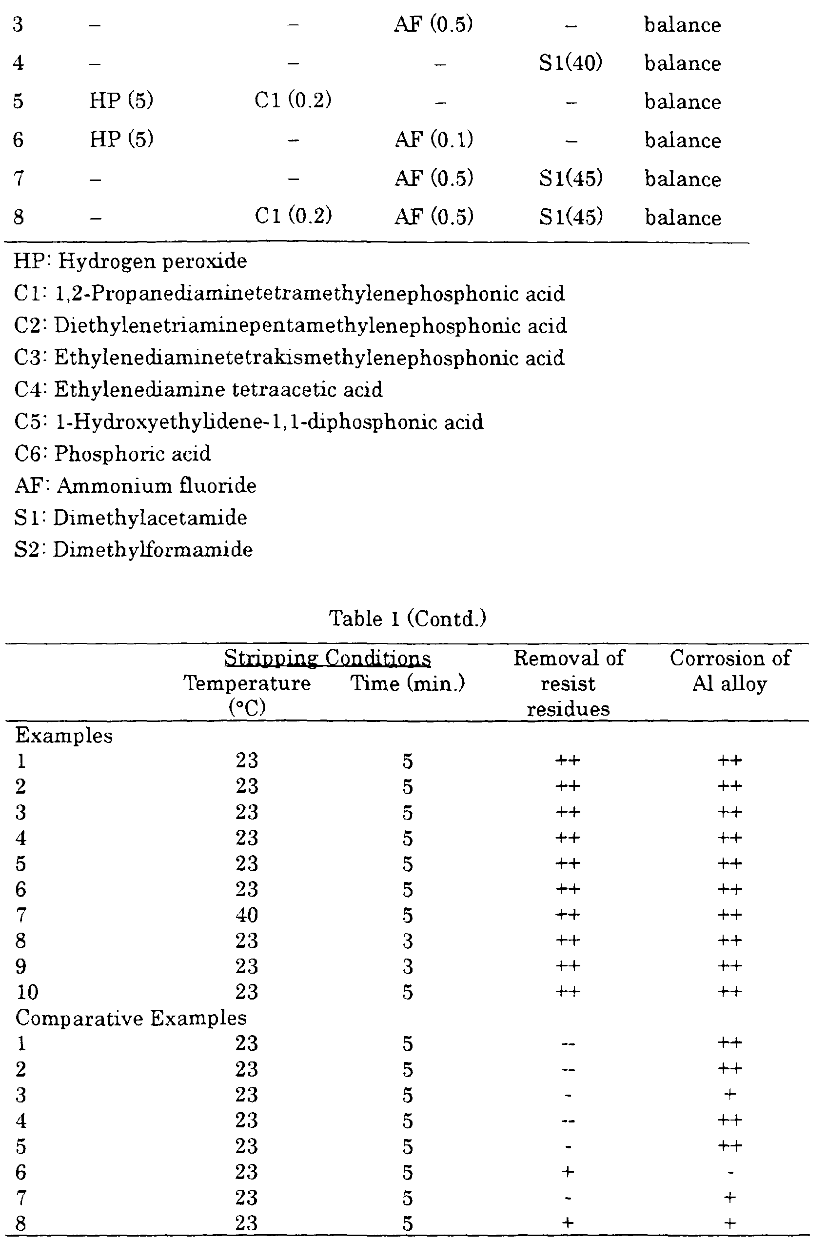
Claims (19)
- An aqueous resist stripping composition containing (a) an oxidizing agent, (b) a chelating agent and (c) a water-soluble fluorine compound.
- An aqueous resist stripping composition containing (a) an oxidizing agent, (b) a chelating agent, (c) a water-soluble fluorine compound and (d) an organic solvent.
- The aqueous resist stripping composition according to claim 1 or 2, wherein said oxidizing agent is at least one oxide selected from the group consisting of hydrogen peroxide, ozone and hypochlorous acid.
- The aqueous resist stripping composition according to claim 1 or 2, wherein said oxidizing agent is hydrogen peroxide
- The aqueous resist stripping composition according to any one of claims 1 to 4, wherein said chelating agent is at least one compound selected from the group consisting of aminopolycarboxylic acids, ammonium salts of the aminopolycaroxylic acids, metal salts of the aminopolycaroxylic acids, organic alkali salts of the aminopolycaroxylic acids, phosphonic chelating agents, ammonium salts of the phosphonic chelating agents, organic amine salts of the phosphonic chelating agents, alkali metal salts of the phosphonic chelating agents, N-oxides of the phosphonic chelating agents, condensed phosphoric acids, ammonium salts of the condensed phosphoric acids, metal salts of the condensed phosphoric acids and organic amine salts of the condensed phosphoric acids.
- The aqueous resist stripping composition according to claim 5, wherein said aminopolycarboxylic acid is at least one compound selected from the group consisting of ethylenediamine tetraacetic acid, dihydroxyethylethylenediaminetetraacetic acid, 1,3-propanedimainetetraacetic acid, diethylenetriaminepentaacetic acid, triethylenetetraminehexaacetic acid, nitrilotriacetic acid and hydroxyethyliminodiacetic acid.
- The aqueous resist stripping composition according to claim 5, wherein said phosphonic chelating agent is at least one compound selected from the group consisting of methyldiphosphonic acid, aminotrismethylenephosphonic acid, ethylidenediphosphonic acid, 1-hydxoxyethylidene-1,1-diphosphonic acid, 1-hydroxypropylidene-1,1-diphosphonic acid, ethylaminobismethylenephosphonic acid, decylaminobismethylenephosphonic acid, nitrilotrismethylenephosphonic acid, ethylenediaminebismethylenephosphonic acid, ethylenedimainetetrakismethylenephosphonic acid, hexanediaminetetrakismethylenephosphonic acid, diethylenetriaminepentamethylenephosphonic acid and 1,2-propanedimainetetramethylenephosphonic acid.
- The aqueous resist stripping composition according to claim 5, wherein said condensed phosphoric acid is at least one compound selected from the group consisting of metaphosphoric acid, tetrametaphosphoric acid, hexametaphosphoric acid and tripolyphosphoric acid.
- The aqueous resist stripping composition according to any one of claims 1 to 4, wherein said chelating agent is a phosphonic chelating agent.
- The aqueous resist stripping composition according to claim 9, wherein said phosphonic chelating agent has 2 to 6 phosphonic acid groups.
- The aqueous resist stripping composition according to claim 9, wherein said phosphonic chelating agent is at least one compound selected from the group consisting of 1,2-propanediaminetetramethylenephosphonic acid, diethylenetriaminepentamethylenephosphonic acid and ethylenediaminetetrakismethylene phosphonic acid.
- The aqueous resist stripping composition according to any one of claims 1 to 11, wherein said water-soluble fluorine compound is at least one compound selected from the group consisting of ammonium fluoride, acid ammonium fluoride, monoethanolamine fluoride and tetramethylammonium fluoride.
- The aqueous resist stripping composition according to any one of claims 1 to 11, wherein said water-soluble fluorine compound is ammonium fluoride.
- The aqueous resist stripping composition according to any one of claims 2 to 13, wherein said organic solvent is at least one solvent selected from the group consisting of ethylene glycol monoethyl ether, ethylene glycol monobutyl ether, diethylene glycol monomethyl ether, diethylene glycol monoethyl ether, diethylene glycol monobutyl ether, propylene glycol monomethyl ether, propylene glycol monoethyl ether, propylene glycol monobutyl ether, dipropylene glycol monomethyl ether, dipropylene glycol monoethyl ether, dipropylene glycol monobutyl ether, diethylene glycol dimethyl ether, dipropylene glycol dimethyl ether, formamide, monomethylformamide, dimethylformamide, monoethylformamide, diethylformamide, acetamide, monoethylacetamide, dimethylacetamide, monoethylacetamide, diethylacetamide, N-methylpyrrolidone, N-ethylpyrrolidone, dimethyl sulfoxide, dimethyl sulfone, diethyl sulfone, bis(2-hydroxy) sulfone and tetramethylene sulfone.
- The aqueous resist stripping composition according to any one of claims 2 to 13, wherein said organic solvent is at least one solvent selected from the group consisting of dimethyl sulfoxide, N,N-dimethylforamide, N,N-dimethylacetamide, N-methylpyrrolidone, diethylene glycol monomethyl ether, diethylene glycol monobutyl ether, dipropylene glycol monomethyl ether and dipropylene glycol monobutyl ether.
- The aqueous resist stripping composition according to any one of claims 1 to 15, comprising (a) 0.0001 to 60 % by weight of said oxidizing agent, (b) 0.01 to 5 % by weight of said chelating agent, (c) 0.00 1 to 10 % by weight of said water-soluble fluorine compound, and balance being water.
- The aqueous resist stripping composition according to any one of claims 2 to 15, comprising (a) 0.0001 to 60 % by weight of said oxidizing agent, (b) 0.01 to 5 % by weight of said chelating agent, (c) 0.001 to 10 % by weight of said water-soluble fluorine compound, (d) 1 to 70 % by weight of said organic solvent, and balance being water.
- A process of stripping resist films and resist residues, comprising the steps of:forming a resist film on an inorganic substrate;patterning the resist film to form a patterned resist film;dry-etching a film underlying the patterned resist film while using the patterned resist film as a mask to remove non-masked regions of the underlying film; andremoving resist residues formed during the dry-etching and/or the patterned resist film remaining after the dry-etching by contacting the resist residues and/or the patterned resist film with an aqueous resist stripping composition according to any one of claims 1 to 17.
- A process of stripping resist films and resist residues, comprising the steps of:forming a resist film on an inorganic substrate;patterning the resist film to form a patterned resist film;dry-etching a film underlying the patterned resist film while using the patterned resist film as a mask to remove non-masked regions of the underlying film;ashing the patterned resist film; andremoving resist residues formed during the dry-etching by contacting the resist residues with an aqueous resist stripping composition according to any one of claims 1 to 17.
Applications Claiming Priority (2)
| Application Number | Priority Date | Filing Date | Title |
|---|---|---|---|
| JP06021999A JP4224652B2 (en) | 1999-03-08 | 1999-03-08 | Resist stripping solution and resist stripping method using the same |
| JP6021999 | 1999-03-08 |
Publications (3)
| Publication Number | Publication Date |
|---|---|
| EP1035446A2 true EP1035446A2 (en) | 2000-09-13 |
| EP1035446A3 EP1035446A3 (en) | 2001-04-18 |
| EP1035446B1 EP1035446B1 (en) | 2009-09-30 |
Family
ID=13135844
Family Applications (1)
| Application Number | Title | Priority Date | Filing Date |
|---|---|---|---|
| EP00103935A Expired - Lifetime EP1035446B1 (en) | 1999-03-08 | 2000-02-25 | Resist stripping composition and process for stripping resist |
Country Status (7)
| Country | Link |
|---|---|
| US (1) | US6323169B1 (en) |
| EP (1) | EP1035446B1 (en) |
| JP (1) | JP4224652B2 (en) |
| KR (1) | KR100694924B1 (en) |
| DE (1) | DE60043034D1 (en) |
| SG (1) | SG76645A1 (en) |
| TW (1) | TW521336B (en) |
Cited By (14)
| Publication number | Priority date | Publication date | Assignee | Title |
|---|---|---|---|---|
| EP1091254A3 (en) * | 1999-09-28 | 2001-05-09 | Mitsubishi Gas Chemical Company, Inc. | Resist stripping composition |
| US6514352B2 (en) * | 2000-10-10 | 2003-02-04 | Tokyo Electron Limited | Cleaning method using an oxidizing agent, chelating agent and fluorine compound |
| WO2003104900A3 (en) * | 2002-06-07 | 2004-02-19 | Mallinckrodt Baker Inc | MICROELECTRONIC CLEANING COMPOSITIONS CONTAINING OXIDANTS AND ORGANIC SOLVENTS |
| WO2004094581A1 (en) * | 2003-04-18 | 2004-11-04 | Ekc Technology, Inc. | Aqueous fluoride compositions for cleaning semiconductor devices |
| US6875288B2 (en) | 2000-10-10 | 2005-04-05 | Tokyo Electron Limited | Cleaning agent and cleaning method |
| WO2005083523A1 (en) * | 2004-02-11 | 2005-09-09 | Mallinckrodt Baker Inc. | Microelectronic cleaning composition containing halogen oxygen acids, salts and derivatives thereof |
| WO2006121580A2 (en) | 2005-05-06 | 2006-11-16 | Mallinckrodt Baker, Inc. | Compositions for the removal of post-etch and ashed photoresist residues and bulk photoresist |
| WO2006107517A3 (en) * | 2005-04-04 | 2006-12-14 | Mallinckrodt Baker Inc | Composition for cleaning ion implanted photoresist in front end of line applications |
| SG129274A1 (en) * | 2003-02-19 | 2007-02-26 | Mitsubishi Gas Chemical Co | Cleaaning solution and cleaning process using the solution |
| WO2010099017A3 (en) * | 2009-02-25 | 2010-10-28 | Mallinckrodt Baker, Inc. | Stripping compositions for cleaning ion implanted photoresist from semiconductor device wafers |
| EP2426705A4 (en) * | 2009-04-30 | 2012-09-26 | Lion Corp | METHOD FOR CLEANING SEMICONDUCTOR SUBSTRATE AND ACID SOLUTION |
| CN103811409A (en) * | 2012-11-12 | 2014-05-21 | 中微半导体设备(上海)有限公司 | A method to enhance the etch selectivity of low dielectric materials to TiN hard mask |
| EP2759881A1 (en) * | 2005-06-07 | 2014-07-30 | Advanced Technology Materials, Inc. | Metal and dielectric compatible sacrificial anti-reflective coating cleaning and removal composition |
| US20230039366A1 (en) * | 2020-04-09 | 2023-02-09 | Showa Denko K.K. | Composition, and method for cleaning adhesive polymer |
Families Citing this family (48)
| Publication number | Priority date | Publication date | Assignee | Title |
|---|---|---|---|---|
| US6831048B2 (en) * | 2000-04-26 | 2004-12-14 | Daikin Industries, Ltd. | Detergent composition |
| US6569252B1 (en) * | 2000-06-30 | 2003-05-27 | International Business Machines Corporation | Semi-aqueous solvent cleaning of paste processing residue from substrates |
| US6762132B1 (en) * | 2000-08-31 | 2004-07-13 | Micron Technology, Inc. | Compositions for dissolution of low-K dielectric films, and methods of use |
| JP2002158206A (en) * | 2000-11-17 | 2002-05-31 | Mitsubishi Electric Corp | Method for removing resist residue and method for manufacturing semiconductor device using the same |
| TW554258B (en) * | 2000-11-30 | 2003-09-21 | Tosoh Corp | Resist stripper |
| JP4525885B2 (en) | 2001-01-12 | 2010-08-18 | 三菱瓦斯化学株式会社 | Photoresist developer and photoresist development method |
| KR100393118B1 (en) * | 2001-02-22 | 2003-07-31 | 현만석 | A method of forming resist patterns in a semiconductor device and a semiconductor washing liquid used in said method |
| US6867148B2 (en) * | 2001-05-16 | 2005-03-15 | Micron Technology, Inc. | Removal of organic material in integrated circuit fabrication using ozonated organic acid solutions |
| JP4285649B2 (en) * | 2001-07-25 | 2009-06-24 | チョン ヨウン カンパニー リミテッド | Surface treatment composition and treatment method for removing silicon component and reducing metal salt generated during etching of aluminum die casting material |
| KR20030011480A (en) * | 2001-08-03 | 2003-02-11 | 주식회사 덕성 | Stripper composition for photoresist |
| JP3797541B2 (en) * | 2001-08-31 | 2006-07-19 | 東京応化工業株式会社 | Photoresist stripping solution |
| JP2003122028A (en) * | 2001-10-17 | 2003-04-25 | Mitsubishi Gas Chem Co Inc | Resist stripper composition |
| TWI276682B (en) * | 2001-11-16 | 2007-03-21 | Mitsubishi Chem Corp | Substrate surface cleaning liquid mediums and cleaning method |
| EP1468335A4 (en) * | 2002-01-11 | 2006-05-17 | Az Electronic Materials Usa | A cleaning agent composition for a positive or a negative photoresist |
| US20030148624A1 (en) * | 2002-01-31 | 2003-08-07 | Kazuto Ikemoto | Method for removing resists |
| US7252718B2 (en) * | 2002-05-31 | 2007-08-07 | Ekc Technology, Inc. | Forming a passivating aluminum fluoride layer and removing same for use in semiconductor manufacture |
| EP1512050A2 (en) * | 2002-06-07 | 2005-03-09 | Mallinckrodt Baker, Inc. | Cleaning compositions for microelectronic substrates |
| JP2004029276A (en) * | 2002-06-25 | 2004-01-29 | Mitsubishi Gas Chem Co Inc | Fluorine-containing resist stripper for copper wiring boards |
| JP2004029346A (en) * | 2002-06-25 | 2004-01-29 | Mitsubishi Gas Chem Co Inc | Resist stripper composition |
| DE10331033B4 (en) * | 2002-07-12 | 2010-04-29 | Ekc Technology K.K. R&D Business Park Bldg. D-3F, Kawasaki | A manufacturing method of a semiconductor device and a cleaning composition therefor |
| JP4443864B2 (en) * | 2002-07-12 | 2010-03-31 | 株式会社ルネサステクノロジ | Cleaning solution for removing resist or etching residue and method for manufacturing semiconductor device |
| JP2009031791A (en) * | 2002-08-14 | 2009-02-12 | Sony Corp | Resist stripper composition and method for manufacturing semiconductor device |
| JP2004133384A (en) | 2002-08-14 | 2004-04-30 | Sony Corp | Resist stripping composition and method for manufacturing semiconductor device |
| KR100464858B1 (en) * | 2002-08-23 | 2005-01-05 | 삼성전자주식회사 | Organic Stripping Composition And Method Of Etching Oxide Using Thereof |
| JP4752270B2 (en) * | 2002-11-08 | 2011-08-17 | 和光純薬工業株式会社 | Cleaning liquid and cleaning method using the same |
| US7101832B2 (en) * | 2003-06-19 | 2006-09-05 | Johnsondiversey, Inc. | Cleaners containing peroxide bleaching agents for cleaning paper making equipment and method |
| KR101117939B1 (en) | 2003-10-28 | 2012-02-29 | 사켐,인코포레이티드 | Cleaning solutions and etchants and methods for using same |
| KR101232249B1 (en) * | 2004-08-10 | 2013-02-12 | 간또 가가꾸 가부시끼가이샤 | Semiconductor substrate cleaning liquid and semiconductor substrate cleaning process |
| JP4254675B2 (en) | 2004-09-29 | 2009-04-15 | カシオ計算機株式会社 | Display panel |
| JP4265515B2 (en) | 2004-09-29 | 2009-05-20 | カシオ計算機株式会社 | Display panel |
| KR101190907B1 (en) * | 2004-12-07 | 2012-10-12 | 가오 가부시키가이샤 | Remover composition |
| JP4637010B2 (en) * | 2004-12-07 | 2011-02-23 | 花王株式会社 | Release agent composition |
| CN1862392B (en) * | 2005-05-13 | 2011-08-03 | 安集微电子(上海)有限公司 | Composition of removing photoresistance layer and use method thereof |
| CN1862391B (en) * | 2005-05-13 | 2013-07-10 | 安集微电子(上海)有限公司 | Composition of removing photoresistance layer and use method thereof |
| US8658053B2 (en) * | 2005-06-24 | 2014-02-25 | Mitsubishi Gas Chemical Company, Inc. | Etching composition for metal material and method for manufacturing semiconductor device by using same |
| JP4734090B2 (en) * | 2005-10-31 | 2011-07-27 | 株式会社東芝 | Manufacturing method of semiconductor device |
| KR101319113B1 (en) * | 2006-04-13 | 2013-10-17 | 동우 화인켐 주식회사 | Cleaner for metal |
| US7591956B2 (en) * | 2006-05-03 | 2009-09-22 | OMG Electronic Chemicals, Inc. | Method and composition for selectively stripping nickel from a substrate |
| WO2008114616A1 (en) | 2007-03-16 | 2008-09-25 | Mitsubishi Gas Chemical Company, Inc. | Cleaning composition and process for producing semiconductor device |
| JP5203637B2 (en) * | 2007-05-07 | 2013-06-05 | イー.ケー.シー.テクノロジー.インコーポレーテッド | Method and composition for removing resist, etching residue, and metal oxide from a substrate having aluminum and aluminum copper alloy |
| CN101755324B (en) * | 2007-07-26 | 2011-10-12 | 三菱瓦斯化学株式会社 | Composition for cleaning and rust prevention and process for producing semiconductor element or display element |
| US7968506B2 (en) * | 2008-09-03 | 2011-06-28 | Taiwan Semiconductor Manufacturing Co., Ltd. | Wet cleaning stripping of etch residue after trench and via opening formation in dual damascene process |
| CN105304485B (en) | 2010-10-06 | 2019-02-12 | 恩特格里斯公司 | Compositions and methods for selectively etching metal nitrides |
| US9593297B2 (en) | 2014-10-15 | 2017-03-14 | Micron Technology, Inc. | Compositions for removing residues and related methods |
| FR3043560B1 (en) * | 2015-11-18 | 2019-12-27 | Arkema France | AQUEOUS HYDROGEN PEROXIDE SOLUTION COMPRISING A SPECIFIC STABILIZER |
| TWI824299B (en) * | 2020-09-22 | 2023-12-01 | 美商恩特葛瑞斯股份有限公司 | Etchant compositions |
| WO2023003215A1 (en) * | 2021-07-21 | 2023-01-26 | 삼성에스디아이 주식회사 | Method of forming patterns |
| CN120769581B (en) * | 2025-09-04 | 2025-11-14 | 合肥晶合集成电路股份有限公司 | A rework method for CIS wafers |
Citations (4)
| Publication number | Priority date | Publication date | Assignee | Title |
|---|---|---|---|---|
| JPS6249355A (en) | 1985-08-10 | 1987-03-04 | Nagase Sangyo Kk | Stripping agent composition |
| JPS6442653A (en) | 1987-08-10 | 1989-02-14 | Tokyo Ohka Kogyo Co Ltd | Peeling solution for positive type photoresist |
| JPH07201794A (en) | 1994-01-07 | 1995-08-04 | Mitsubishi Gas Chem Co Inc | Semiconductor device cleaning agent and method of manufacturing semiconductor device |
| JPH0820205A (en) | 1994-07-08 | 1996-01-23 | Bridgestone Corp | Pneumatic radial tires |
Family Cites Families (14)
| Publication number | Priority date | Publication date | Assignee | Title |
|---|---|---|---|---|
| US3841905A (en) * | 1970-11-19 | 1974-10-15 | Rbp Chem Corp | Method of preparing printed circuit boards with terminal tabs |
| DE2141235C3 (en) * | 1971-08-17 | 1980-08-07 | Siemens Ag, 1000 Berlin Und 8000 Muenchen | Etchant for metal-coated silicon semiconductor wafers |
| JPH01272785A (en) * | 1988-04-25 | 1989-10-31 | Nippon Hyomen Kagaku Kk | Method for chemically polishing titanium or titanium alloy |
| JPH03237007A (en) * | 1990-02-13 | 1991-10-22 | Mitsubishi Gas Chem Co Inc | Hydrogen peroxide composition |
| US5466389A (en) * | 1994-04-20 | 1995-11-14 | J. T. Baker Inc. | PH adjusted nonionic surfactant-containing alkaline cleaner composition for cleaning microelectronics substrates |
| JP3255551B2 (en) | 1995-01-31 | 2002-02-12 | 東京応化工業株式会社 | Stripper composition for resist |
| JP2911792B2 (en) * | 1995-09-29 | 1999-06-23 | 東京応化工業株式会社 | Stripper composition for resist |
| US5700383A (en) * | 1995-12-21 | 1997-12-23 | Intel Corporation | Slurries and methods for chemical mechanical polish of aluminum and titanium aluminide |
| JP3690619B2 (en) * | 1996-01-12 | 2005-08-31 | 忠弘 大見 | Cleaning method and cleaning device |
| DE69729553T2 (en) * | 1996-03-22 | 2005-08-18 | Merck Patent Gmbh | SOLUTIONS AND METHODS FOR REMOVING SIDE DEPOSITS AFTER A DRY STEP |
| TW416987B (en) * | 1996-06-05 | 2001-01-01 | Wako Pure Chem Ind Ltd | A composition for cleaning the semiconductor substrate surface |
| KR100248113B1 (en) * | 1997-01-21 | 2000-03-15 | 이기원 | Cleaning and Etching Compositions for Electronic Displays and Substrates |
| US5981401A (en) * | 1998-03-13 | 1999-11-09 | Micron Technology, Inc. | Method for selective etching of anitreflective coatings |
| JPH11340182A (en) * | 1998-05-25 | 1999-12-10 | Wako Pure Chem Ind Ltd | Cleaning agent for semiconductor surface, and method for cleaning |
-
1999
- 1999-03-08 JP JP06021999A patent/JP4224652B2/en not_active Expired - Lifetime
-
2000
- 2000-02-24 SG SG200000943A patent/SG76645A1/en unknown
- 2000-02-25 DE DE60043034T patent/DE60043034D1/en not_active Expired - Lifetime
- 2000-02-25 EP EP00103935A patent/EP1035446B1/en not_active Expired - Lifetime
- 2000-03-02 TW TW089103662A patent/TW521336B/en not_active IP Right Cessation
- 2000-03-03 US US09/517,592 patent/US6323169B1/en not_active Expired - Lifetime
- 2000-03-03 KR KR1020000010703A patent/KR100694924B1/en not_active Expired - Lifetime
Patent Citations (4)
| Publication number | Priority date | Publication date | Assignee | Title |
|---|---|---|---|---|
| JPS6249355A (en) | 1985-08-10 | 1987-03-04 | Nagase Sangyo Kk | Stripping agent composition |
| JPS6442653A (en) | 1987-08-10 | 1989-02-14 | Tokyo Ohka Kogyo Co Ltd | Peeling solution for positive type photoresist |
| JPH07201794A (en) | 1994-01-07 | 1995-08-04 | Mitsubishi Gas Chem Co Inc | Semiconductor device cleaning agent and method of manufacturing semiconductor device |
| JPH0820205A (en) | 1994-07-08 | 1996-01-23 | Bridgestone Corp | Pneumatic radial tires |
Cited By (26)
| Publication number | Priority date | Publication date | Assignee | Title |
|---|---|---|---|---|
| US6372410B1 (en) | 1999-09-28 | 2002-04-16 | Mitsubishi Gas Chemical Company, Inc. | Resist stripping composition |
| EP1091254A3 (en) * | 1999-09-28 | 2001-05-09 | Mitsubishi Gas Chemical Company, Inc. | Resist stripping composition |
| US6514352B2 (en) * | 2000-10-10 | 2003-02-04 | Tokyo Electron Limited | Cleaning method using an oxidizing agent, chelating agent and fluorine compound |
| US6875288B2 (en) | 2000-10-10 | 2005-04-05 | Tokyo Electron Limited | Cleaning agent and cleaning method |
| WO2003104900A3 (en) * | 2002-06-07 | 2004-02-19 | Mallinckrodt Baker Inc | MICROELECTRONIC CLEANING COMPOSITIONS CONTAINING OXIDANTS AND ORGANIC SOLVENTS |
| SG129274A1 (en) * | 2003-02-19 | 2007-02-26 | Mitsubishi Gas Chemical Co | Cleaaning solution and cleaning process using the solution |
| WO2004094581A1 (en) * | 2003-04-18 | 2004-11-04 | Ekc Technology, Inc. | Aqueous fluoride compositions for cleaning semiconductor devices |
| CN101833251B (en) * | 2004-02-11 | 2013-11-13 | 安万托特性材料股份有限公司 | Microelectronic cleaning composition containing halogen oxygen acids, salts and derivatives thereof |
| EP1564595A3 (en) * | 2004-02-11 | 2007-06-27 | Mallinckrodt Baker, Inc. | Composition for cleaning microelectronic substrates containing halogen oxygen acids and derivatives thereof |
| CN1954267B (en) * | 2004-02-11 | 2010-12-08 | 马林克罗特贝克公司 | Microelectronic cleaning compositions containing halogen oxyacids, salts and derivatives thereof |
| WO2005083523A1 (en) * | 2004-02-11 | 2005-09-09 | Mallinckrodt Baker Inc. | Microelectronic cleaning composition containing halogen oxygen acids, salts and derivatives thereof |
| WO2006107517A3 (en) * | 2005-04-04 | 2006-12-14 | Mallinckrodt Baker Inc | Composition for cleaning ion implanted photoresist in front end of line applications |
| US8044009B2 (en) | 2005-04-04 | 2011-10-25 | Avantor Performance Materials, Inc. | Compositions for cleaning ion implanted photoresist in front end of line applications |
| CN101171551B (en) * | 2005-05-06 | 2012-12-26 | 安万托特性材料股份有限公司 | Composition for removing post-etch and ashed photoresist residues and most photoresists |
| WO2006121580A3 (en) * | 2005-05-06 | 2007-02-15 | Mallinckrodt Baker Inc | Compositions for the removal of post-etch and ashed photoresist residues and bulk photoresist |
| WO2006121580A2 (en) | 2005-05-06 | 2006-11-16 | Mallinckrodt Baker, Inc. | Compositions for the removal of post-etch and ashed photoresist residues and bulk photoresist |
| US7754668B2 (en) | 2005-05-06 | 2010-07-13 | Mallinckrodt Baker. Inc | Compositions for the removal of post-etch and ashed photoresist residues and bulk photoresist |
| EP2759881A1 (en) * | 2005-06-07 | 2014-07-30 | Advanced Technology Materials, Inc. | Metal and dielectric compatible sacrificial anti-reflective coating cleaning and removal composition |
| US8951948B2 (en) | 2005-06-07 | 2015-02-10 | Advanced Technology Materials, Inc. | Metal and dielectric compatible sacrificial anti-reflective coating cleaning and removal composition |
| US9422513B2 (en) | 2005-06-07 | 2016-08-23 | Advanced Technology Materials, Inc. | Metal and dielectric compatible sacrificial anti-reflective coating cleaning and removal composition |
| WO2010099017A3 (en) * | 2009-02-25 | 2010-10-28 | Mallinckrodt Baker, Inc. | Stripping compositions for cleaning ion implanted photoresist from semiconductor device wafers |
| EP2426705A4 (en) * | 2009-04-30 | 2012-09-26 | Lion Corp | METHOD FOR CLEANING SEMICONDUCTOR SUBSTRATE AND ACID SOLUTION |
| CN103811409A (en) * | 2012-11-12 | 2014-05-21 | 中微半导体设备(上海)有限公司 | A method to enhance the etch selectivity of low dielectric materials to TiN hard mask |
| CN103811409B (en) * | 2012-11-12 | 2016-04-20 | 中微半导体设备(上海)有限公司 | Method for enhancing etching selectivity of low dielectric material to TiN hard mask |
| US20230039366A1 (en) * | 2020-04-09 | 2023-02-09 | Showa Denko K.K. | Composition, and method for cleaning adhesive polymer |
| US12577508B2 (en) * | 2020-04-09 | 2026-03-17 | Resonac Corporation | Composition, and method for cleaning adhesive polymer |
Also Published As
| Publication number | Publication date |
|---|---|
| SG76645A1 (en) | 2000-11-21 |
| KR20000076769A (en) | 2000-12-26 |
| DE60043034D1 (en) | 2009-11-12 |
| EP1035446A3 (en) | 2001-04-18 |
| US6323169B1 (en) | 2001-11-27 |
| TW521336B (en) | 2003-02-21 |
| KR100694924B1 (en) | 2007-03-14 |
| EP1035446B1 (en) | 2009-09-30 |
| JP2000258924A (en) | 2000-09-22 |
| JP4224652B2 (en) | 2009-02-18 |
Similar Documents
| Publication | Publication Date | Title |
|---|---|---|
| US6323169B1 (en) | Resist stripping composition and process for stripping resist | |
| US6686322B1 (en) | Cleaning agent and cleaning process using the same | |
| KR100813753B1 (en) | Cleaning method | |
| JP3150306B2 (en) | Detergent composition containing nucleophilic amine compound having reduction and oxidation potential and method for cleaning substrate using the same | |
| KR100319881B1 (en) | Aqueous cleaning solution for removing contaminants from surface of integrated circuit substrate and cleaning method using thereof | |
| US20090120457A1 (en) | Compositions and method for removing coatings and preparation of surfaces for use in metal finishing, and manufacturing of electronic and microelectronic devices | |
| US20040147421A1 (en) | Process for the use of bis-choline and tris-choline in the cleaning of quartz-coated polysilicon and other materials | |
| US20090291565A1 (en) | Method for stripping photoresist | |
| EP1488286A1 (en) | Ph buffered compositions for cleaning semiconductor substrates | |
| KR20040032855A (en) | Sulfoxide Pyrolid(in)one Alkanolamine Stripping and Cleaning Composition | |
| KR20010024240A (en) | Process for removing residues from a semiconductor substrate | |
| EP2034365A2 (en) | Microelectronic cleaning compositions containing oxidizers and organic solvents | |
| KR100640107B1 (en) | Cleaning composition for removing resists and manufacturing method of semiconductor device | |
| JP4374989B2 (en) | Cleaning liquid and cleaning method using the same | |
| US20050089489A1 (en) | Composition for exfoliation agent effective in removing resist residues | |
| JP3968535B2 (en) | Manufacturing method of semiconductor device | |
| JP3820545B2 (en) | Resist stripping composition and method for manufacturing semiconductor device using the same | |
| KR19990007139A (en) | Photoresist Peeling Composition | |
| JP4355083B2 (en) | Photoresist stripping composition and semiconductor substrate processing method using the same | |
| JP2005223030A (en) | Semiconductor substrate cleaning agent and cleaning method thereof | |
| JP4122171B2 (en) | Resist residue remover or cleaning agent for semiconductor device or liquid crystal device manufacturing process | |
| KR20010031136A (en) | Ammonium borate containing compositions for stripping residues from semiconductor substrates | |
| JP5206177B2 (en) | Resist stripping composition and method for manufacturing semiconductor device using the same | |
| TW202444877A (en) | Composition for tin hard mask removal while compatible with tungsten | |
| JP2000171985A (en) | Liquid crystal panel substrate cleaning method |
Legal Events
| Date | Code | Title | Description |
|---|---|---|---|
| PUAI | Public reference made under article 153(3) epc to a published international application that has entered the european phase |
Free format text: ORIGINAL CODE: 0009012 |
|
| AK | Designated contracting states |
Kind code of ref document: A2 Designated state(s): DE FR GB |
|
| AX | Request for extension of the european patent |
Free format text: AL;LT;LV;MK;RO;SI |
|
| PUAL | Search report despatched |
Free format text: ORIGINAL CODE: 0009013 |
|
| AK | Designated contracting states |
Kind code of ref document: A3 Designated state(s): AT BE CH CY DE DK ES FI FR GB GR IE IT LI LU MC NL PT SE |
|
| AX | Request for extension of the european patent |
Free format text: AL;LT;LV;MK;RO;SI |
|
| 17P | Request for examination filed |
Effective date: 20010921 |
|
| AKX | Designation fees paid |
Free format text: DE FR GB |
|
| 17Q | First examination report despatched |
Effective date: 20070123 |
|
| GRAP | Despatch of communication of intention to grant a patent |
Free format text: ORIGINAL CODE: EPIDOSNIGR1 |
|
| GRAS | Grant fee paid |
Free format text: ORIGINAL CODE: EPIDOSNIGR3 |
|
| GRAA | (expected) grant |
Free format text: ORIGINAL CODE: 0009210 |
|
| AK | Designated contracting states |
Kind code of ref document: B1 Designated state(s): DE FR GB |
|
| REG | Reference to a national code |
Ref country code: GB Ref legal event code: FG4D |
|
| REF | Corresponds to: |
Ref document number: 60043034 Country of ref document: DE Date of ref document: 20091112 Kind code of ref document: P |
|
| PLBE | No opposition filed within time limit |
Free format text: ORIGINAL CODE: 0009261 |
|
| STAA | Information on the status of an ep patent application or granted ep patent |
Free format text: STATUS: NO OPPOSITION FILED WITHIN TIME LIMIT |
|
| 26N | No opposition filed |
Effective date: 20100701 |
|
| PGFP | Annual fee paid to national office [announced via postgrant information from national office to epo] |
Ref country code: FR Payment date: 20110218 Year of fee payment: 12 Ref country code: DE Payment date: 20110223 Year of fee payment: 12 |
|
| PGFP | Annual fee paid to national office [announced via postgrant information from national office to epo] |
Ref country code: GB Payment date: 20110223 Year of fee payment: 12 |
|
| GBPC | Gb: european patent ceased through non-payment of renewal fee |
Effective date: 20120225 |
|
| REG | Reference to a national code |
Ref country code: FR Ref legal event code: ST Effective date: 20121031 |
|
| REG | Reference to a national code |
Ref country code: DE Ref legal event code: R119 Ref document number: 60043034 Country of ref document: DE Effective date: 20120901 |
|
| PG25 | Lapsed in a contracting state [announced via postgrant information from national office to epo] |
Ref country code: GB Free format text: LAPSE BECAUSE OF NON-PAYMENT OF DUE FEES Effective date: 20120225 Ref country code: FR Free format text: LAPSE BECAUSE OF NON-PAYMENT OF DUE FEES Effective date: 20120229 |
|
| PG25 | Lapsed in a contracting state [announced via postgrant information from national office to epo] |
Ref country code: DE Free format text: LAPSE BECAUSE OF NON-PAYMENT OF DUE FEES Effective date: 20120901 |