EP1035421A2 - Method and apparatus for reading a solid state radiation image - Google Patents
Method and apparatus for reading a solid state radiation image Download PDFInfo
- Publication number
- EP1035421A2 EP1035421A2 EP00103273A EP00103273A EP1035421A2 EP 1035421 A2 EP1035421 A2 EP 1035421A2 EP 00103273 A EP00103273 A EP 00103273A EP 00103273 A EP00103273 A EP 00103273A EP 1035421 A2 EP1035421 A2 EP 1035421A2
- Authority
- EP
- European Patent Office
- Prior art keywords
- radiation
- voltage
- emission
- detector
- light
- Prior art date
- Legal status (The legal status is an assumption and is not a legal conclusion. Google has not performed a legal analysis and makes no representation as to the accuracy of the status listed.)
- Granted
Links
- 230000005855 radiation Effects 0.000 title claims abstract description 220
- 238000000034 method Methods 0.000 title claims description 97
- 239000007787 solid Substances 0.000 title claims description 60
- 238000001514 detection method Methods 0.000 claims description 23
- 230000006870 function Effects 0.000 claims description 7
- 230000005611 electricity Effects 0.000 description 28
- 238000006243 chemical reaction Methods 0.000 description 21
- 238000010586 diagram Methods 0.000 description 10
- 230000003287 optical effect Effects 0.000 description 8
- 238000010276 construction Methods 0.000 description 5
- 230000002265 prevention Effects 0.000 description 4
- 230000000994 depressogenic effect Effects 0.000 description 3
- 230000000694 effects Effects 0.000 description 3
- 230000006798 recombination Effects 0.000 description 3
- 238000005215 recombination Methods 0.000 description 3
- 229910021417 amorphous silicon Inorganic materials 0.000 description 2
- 239000004020 conductor Substances 0.000 description 2
- 230000005684 electric field Effects 0.000 description 2
- 230000004044 response Effects 0.000 description 2
- 239000000126 substance Substances 0.000 description 2
- 239000012212 insulator Substances 0.000 description 1
- 239000000463 material Substances 0.000 description 1
- 239000002184 metal Substances 0.000 description 1
- 230000007935 neutral effect Effects 0.000 description 1
- 230000002093 peripheral effect Effects 0.000 description 1
- 239000004065 semiconductor Substances 0.000 description 1
- 239000010409 thin film Substances 0.000 description 1
- 230000002463 transducing effect Effects 0.000 description 1
Images



Classifications
-
- G—PHYSICS
- G01—MEASURING; TESTING
- G01T—MEASUREMENT OF NUCLEAR OR X-RADIATION
- G01T1/00—Measuring X-radiation, gamma radiation, corpuscular radiation, or cosmic radiation
- G01T1/16—Measuring radiation intensity
- G01T1/24—Measuring radiation intensity with semiconductor detectors
- G01T1/246—Measuring radiation intensity with semiconductor detectors utilizing latent read-out, e.g. charge stored and read-out later
Definitions
- the resultant signal charge is temporarily stored in the electricity storage portion of the photoelectric conversion element, and the stored charge is converted to an image signal (electric signal) and is output.
- an image signal electric signal
- There is also a solid radiation detector of direct conversion type see “MATERIAL PARAMETERS IN THICK HYDROGENATED AMORPHOUS SILICON RADIATION DETECTOR,” Lawrence Berkeley Laboratory and University of California, Berkeley, CA 94720 Xerox Parc, Palo Alto, CA 94304, "Metal/Amorphous Silicon Multilayer Radiation Detectors,” IEE TRANSACTION ON NUCLEAR SCIENCE, Vol. 36, NO.2 April 1989, Japanese Unexamined Patent Publication No. 1(1989)-216290, etc.).
- a signal charge, produced in a radiation conductor irradiated with radiation is collected by a charge collecting electrode and is temporarily stored in an electricity storage portion. The stored charge is converted to an electric signal and is output.
- TFT thin-film transistor
- the improved solid radiation detector is of a direct conversion and optical reading type and is formed by stacking (1) a recording photoconductive layer which exhibits photoconductivity by receiving the emission of recording radiation directly or indirectly, (2) a charge transfer layer which operates as substantially an electric conductor with respect to an electric charge of the same polarity as a latent image charge and also operates as substantially an insulator with respect to a transfer charge of the opposite polarity from the latent image charge, and (3) a reading photoconductive layer which exhibits photoconductivity by receiving the emission of a reading electromagnetic wave, in the recited order.
- a signal charge (latent image charge) carrying image information is stored in the interface (electricity storage portion) between the recording photoconductive layer and the charge transfer layer. Also, electrodes (first and second conductive layers) are stacked on both sides of these 3 layers. The recording photoconductive layer, the charge transfer layer, and the reading photoconductive layer form the major part of the solid radiation detector in this type.
- a predetermined voltage is applied across the above-mentioned detector (which is, for example, a solid detector such as a photoelectric conversion element) to emit radiation, whereby an electric charge representing radiation-image information is stored in the electricity storage portion.
- the application of voltage is stopped, or a standby voltage less than the above-mentioned predetermined voltage is applied. In this way, the electric charge stored in the electricity storage portion is held and the occurrence of dark current, which will be caused by continuing to apply the aforementioned predetermined voltage, is prevented.
- Some of the direct conversion type detectors can perform recording immediately after dc voltage has been applied between both ends of the detector to form a predetermined electric field within the detector, as described in the above-mentioned Japanese Unexamined Patent Publication No. 10(1998)-271374, and others need to perform real recording after the detector has been pre-charged by primary exposure before recording, as described in "23027 Method and device for recording and transducing an electromagnetic energy pattern (Research Disclosure, June 1983)", for example.
- some of the light conversion type detectors need to supply a predetermined electric charge to the electricity storage portion in advance to fully charge the electricity storage portion prior to photographing.
- Japanese Unexamined Patent Publication No. 8(1996)-271374 discloses that the X-rays transmitted through the solid radiation detector are detected with an X-ray sensor provided behind the detector and, based on the result of detection, the amount of the transmitted X-rays is controlled.
- an X-ray sensor provided behind the detector and, based on the result of detection, the amount of the transmitted X-rays is controlled.
- the primary object of the present invention is to provide a radiation-image photographing method and apparatus which is capable of performing the application of voltage to the solid radiation detector, the emission of recording radiation or preexposure light, etc. at appropriate timings.
- preexposure in the case of using an optical reading type detector, it is desirable, from the viewpoint of the removal of an unnecessary electric charge in addition to the above-mentioned timings, that preexposure be started near the start of voltage application to the detector. That is, it is desirable that the application of voltage to the detector and the start of preexposure light emission be performed at almost the same time.
- preexposure is continued up to just before the start of radiation emission.
- a first radiation-image photographing method is a radiation-image photographing method for obtaining radiation-image information of a subject, the method comprising the steps of:
- a second radiation-image photographing method is a radiation-image photographing method for obtaining radiation-image information of a subject, the method comprising the steps of:
- a first radiation-image photographing apparatus is a radiation-image photographing apparatus for obtaining radiation-image information of a subject, the apparatus comprising:
- the apparatus further comprises detection means for detecting the presence of the emission of the radiation, and the control means starts the application of the voltage when the detection means detects that the emission of the radiation is present, and/or stops the application of the voltage when the detection means detects no emission of the radiation after the radiation has been emitted.
- any type of detection means may be used, as long as it is able to detect the presence of radiation, transmitted through a subject and incident on the detector, or detect what is in a corresponding relationship with the radiation.
- the detection means is not limited to detecting radiation itself transmitted through a subject, but may be any detector which detects radiation emitted from the radiation source corresponding to the radiation incident on the detector or may be any detector that detects light issuing from the detector irradiated with radiation. For instance, a photo timer, a photodiode and the like are preferred. Note that because current flows in the detector when recording radiation is emitted to the detector, the detector itself can function as the detection means for detecting the presence of the emission of radiation.
- a second radiation-image photographing apparatus is a radiation-image photographing apparatus for obtaining radiation-image information of a subject, the apparatus comprising:
- the apparatus further comprises detection means for detecting the presence of the emission of the electromagnetic wave, and the control means starts the application of the voltage when the detection means detects that the emission of the electromagnetic wave is present, and/or starts the emission of the radiation when the detection means detects no emission of the electromagnetic after the electromagnetic wave has been emitted.
- the "emission of recording radiation” in the above-mentioned methods and apparatuses means that the radiation representative of the radiation-image information on a subject, emitted from the radiation source and transmitted through the subject, is emitted to the detector.
- the "application of voltage to the solid radiation detector which is required for storing an electric charge representative of radiation-image information in the solid detecting elements” means that necessary voltage is applied to the detector to store an electric charge representative of radiation-image information, generated in the charge generating portions of the solid detecting elements of the detector by emitting the recording radiation to the detector, in the electricity storage portions of the solid detecting elements.
- the application of voltage is not limited to the application of a desired voltage to a solid detecting element such as a photoelectric conversion element but includes the application of a desired voltage to other portions of the detector necessary for the aforementioned storage.
- the "emission of an electromagnetic wave for preexposure” means emitting an electromagnetic wave other than recording light and reading light to the recording surface side or reading surface side of the detector prior to the emission of the recording light to the detector
- the phrase "almost the same time” in the above-mentioned methods and apparatuses means the relation of time that the start and stop of voltage application to the solid radiation detector, the start and stop of radiation emission, and the start and stop of electromagnetic wave emission for preexposure are performed at the aforementioned respective appropriate timings.
- the phrase “almost the same time” is sufficient if it is the above-mentioned appropriate timing, and does not always need to be at exactly the same time.
- the detector which is used in the method and apparatus of the present invention, may be of any type and can use detectors of various types, such as the above-mentioned light conversion type, direct conversion type, TFT reading type, optical reading type, improved direct conversion type which is a combination of them, and the like.
- the appropriate timings of the start of voltage application and the start of radiation emission vary depending on detectors to be used. Therefore, it is a matter of course that the application of voltage and the like need to be performed at appropriate timings in accordance with a detector to be used.
- the timing control (time management) method for performing the start of voltage application and the start of radiation emission and the like at almost the same time may be any method, if it can automatically perform start and stop operations so that the start of voltage application and the start of radiation emission and the like are performed at the above-mentioned appropriate timings. For instance, based on a photographing start instruction from an operator, a timer can be started so that the start and stop of voltage application, emission of radiation and the like are performed at respective set times.
- respective timings are caused to automatically coincide with each other so that the start of voltage application to the solid radiation detector and the start of recording radiation emission are performed at almost the same time, or so that the stop of voltage application and the stop of radiation emission are performed at almost the same time. Therefore, an electric charge corresponding to the ray amount of the recording radiation can be stored after an unnecessary electric charge remaining within the detector has been removed.
- the possibility of giving rise to the problems of the increase of dark current and an unremoved unnecessary electric charge is reduced, so that a S/N ratio in an image, reproduced based on an image signal output from the detector, can be improved compared with manual operation.
- the conventional apparatus does not necessarily perform operations at appropriate timing from the viewpoint of the occurrence prevention of dark current, removal of an unnecessary electric charge, and full charging, whereas the present invention can reduce the possibility of increasing noise in an image signal and can improve a S/N ratio in an reproduced image, because respective timings are caused to automatically coincide with each other so that the application stop of voltage and the emission stop of recording radiation are performed at nearly the same time.
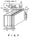
- the radiation detector 10 is an electrostatic recording device of the improved direct conversion type (direct conversion and optical reading type) described in the aforementioned Japanese Unexamined Patent Publication No. 10(1998)-232824.
- Radiation for recording e.g., X-rays or the like which will hereinafter be referred to as recording light
- recording light Radiation for recording
- the produced electric charge is stored as a latent image charge in an electricity storage portion 16 which is the interface between the recording photoconductive layer 12 and a charge transfer layer 13.
- a second conductive layer 15 is scanned with an electromagnetic wave for reading (hereinafter called reading light), whereby an electric charge is produced within a reading photoconductive layer 14.
- the produced electric charge recombines with the aforementioned latent image charge, thereby generating current corresponding to the amount of the latent image charge.
- the second conductive layer 15 as a reading electrode is formed by a large number of line electrodes (shaded by oblique lines in Fig. 1) arrayed in stripe form.
- the line electrodes of the second conductive layer 15 will hereinafter be referred to as a stripe electrode 15 and each line electrode as an element 15a.
- the surface light source 30 is an electroluminescent (EL) body comprising a first conductive layer 31, an EL layer 32, and a second conductive layer 33, and as described above, the surface light source 30 is stacked on the radiation detector 10. Between the stripe electrode 15 of the radiation detector 10 and the first conductive layer 31 of the surface light source 30, there is provided an insulating layer 34.
- the first conductive layer 31 of the surface light source 30 is formed by a large number of elements 31a (shaded by oblique lines in Fig. 1) arrayed in the form of a stripe, each element 31a being arrayed so as to cross each element 15a of the stripe electrode 15 of the detector 10. In this embodiment, the elements 15a and 31a cross at substantially right angles. In this way, a large number of line light sources 31a are arrayed in surface form. Each element 31a is connected to the light-source control means 40.
- the light-source control means 40 applies a predetermined voltage between the element 31a and the opposite conductive layer 33. More specifically, the control means 40 individually applies voltage to the element 31a during reading and applies voltage to a plurality of or all elements 31a at the same time during preexposure. For instance, if a predetermined dc voltage is applied between each element 31a and the conductive layer 32, while the element 31a is being switched in sequence, EL light is issued from the EL layer 32 sandwiched between the element 31a and the conductive layer 33, and the EL light transmitted through the element 31a is utilized as reading light in the form of a line (hereinafter referred to as line light).
- line light a line
- the surface light source 30 becomes equivalent to a large number of small line light sources arrayed in surface form, and by sequentially switching all the elements 31a from one end in the longitudinal of the stripe electrode 15 to the other end and emitting EL light, the entire surface of the stripe electrode 15 can be electrically scanned with the line light.
- the longitudinal direction of the element 15a corresponds to a vertical scanning direction
- the extending direction of the line light corresponds to a horizontal scanning direction.
- EL light is emitted substantially uniformly from the EL layer 32 over the entire surface of the stripe electrode 15 by this application of voltage.
- This EL light is utilized as an electromagnetic wave for preexposure (hereinafter referred to as preexposure light). That is, the surface light source 30 is constructed to function not only as a reading light source but also as a preexposure light source.
- a control signal C1 is input to the light-source control means 40.
- the light-source control means 40 goes to a preexposure mode when the control signal C1 is low and goes to a recording light mode when the signal C1 is high.
- the control signal C1 is in a high impedance state, no EL light is issued from the surface light source 30.
- the radiation emitting section 60 comprises a radiation source 61 for emitting radiation R, a high-voltage generator 62 for generating electric power which drives the radiation source 61, and a generator switch 63 connected to the high-voltage generator 62 to control photographing.
- the generator switch 63 is a two-stage switch consisting of a first generator switch 63a and a second generator switch 63b and is constructed such that unless the first generator 63a is on, the second generator switch 63b is not made on.
- the high-voltage generator 62 is provided with a timer by which the time t 01 of emitting recording light can be set.
- control means 70 does not function, i.e., in the case where the apparatus 1 is assumed to be the same as the aforementioned conventional apparatus.
- the control signal C1 input to the light-source control means 40 is made low (preexposure mode) and preexposure is performed, whereby an unnecessary electric charge stored in the electricity storage portion 16 is discharged.
- the voltage controlling switch 52 may be in any state.
- control signal C1 is caused to be in a high impedance state to stop preexposure and also the second generator switch 63b is made on, after a standby lamp (not shown) provided in the high-voltage generator 62 has been lit and the high voltage HV has become stable, the stable high voltage HV is supplied from the high-voltage generator 62 to the radiation source 61 and therefore radiation R is emitted from the radiation source 61.
- This radiation R is incident onto the subject 65, and the recording light Q, transmitted through the subject 65 and carrying the radiation-image information of the subject 65, is emitted to the detector 10 by the emission time t 01 set by the timer (not shown) of the high-voltage generator 62.
- the control signal C1 is first made high (recording-light mode) and the voltage controlling switch 52 is connected to the conductive layer 11 side of the detector 10. While the element 31a is being switched in sequence, a predetermined dc voltage is applied between each element 31a and the conductive layer 33 by the light control means 40, and the entire surface of the detector 10 is electrically scanned with the line light issued from the EL layer 32.
- This current is simultaneously detected by each current detecting amplifier 51 connected to the corresponding element 15a.
- the current flowing in the detector 10 during reading operation corresponds to the latent image charge, i.e., the electrostatic latent image, and therefore the electrostatic latent image is read out by detecting this current. That is, an image signal representing the electrostatic latent image can be acquired.
- the preexposure, recording, and reading operations are all performed based on the manual switching of switches and control signals by the operator and these operations are not always performed at proper timings from the aspect of the prevention of dark current, the removal of an unnecessary electric charge and the like. For this reason, for example, there is a problem that (1) it takes a long period of time until recording radiation is emitted from the stop of preexposure and (2) if dc voltage is still being applied across the detector 10 after the end of recording, then an unnecessary electric charge will be produced within the detector 10, the noise in the image signal output from the detector 10 will be increased, and the S/N ratio in the reproduced image will be reduced.
- control means 70 is provided for performing timing control so that the start and stop of voltage application to the detector 10, the start and stop of preexposure light emission, and the start and stop of the recording light emission are performed at respective predetermined timings, and as the peripheral components, a sensor 72 for sensing the presence of recording light and the like are provided.
- the control means 70 receives signals S1, S2 from the generator switches 63a, 63b, a signal S3 from the sensor 72, and a standby signal S4, emission end signal S5, and signal S6, which indicates the set emission time t on of emitting recording light, from the high-voltage generator 62.
- the control means 70 also outputs a control signal C1 to the light-source control means 40, a control signal C2 to the voltage controlling switch 52, and a control signal C3 to the high-voltage generator 62.
- the control signal C2 is high, the voltage controlling switch 52 is switched to the power source 53 side and dc voltage is applied from the power source 53 across the detector 10 (i.e., between the conductive layer 11 and stripe electrode 15 of the detector 10).
- the voltage controlling switch 52 When the control signal C2 is in a high impedance state, on the other hand, the voltage controlling switch 52 is set to its neutral point, the positive polarity of the power source 53 goes to a floating state, and no voltage is applied to the detector 10. Furthermore, when the control signal C2 is low, the voltage controlling switch 52 is switched to the conductive layer 11 side of the detector 10.
- the high-voltage generator 62 supplies high voltage HV to the radiation source 61 when the control signal C3 is input as a logic high signal, and therefore the radiation source 61 is caused to emit radiation R.
- the sensor 72 can use a photo timer which detects the amount of recording light (recording radiation). This sensor 72 may be provided integrally with or separately from the detector 10. The sensor 72 may detect the recording light Q transmitted through the subject 65, or may detect the radiation R emitted from the radiation source 61.
- the control means 70 is provided with a timer (not shown) so that it can issue control signals C1 to C3 after the lapse of a predetermined time. Note that some of the control signals C1 to C3 are issued according to embodiments of a control method to be described later and therefore all the control signals C1 to C3 are not always issued. Also, some of the signals S1, S2, . . . S8 to be input the control signal 70 are issued according to the embodiments of the control method to be described later and therefore all the signals are not necessarily issued.
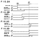
- Fig. 2A is a timing chart showing a first method of the voltage-application/recording-light start control. This first method performs control, with the ON operation of the first generator switch 63a as a trigger.
- the high-voltage generator 62 When the first generator switch 63a is first switched on manually by the operator, the high-voltage generator 62 generates high voltage HV (the same applies for the other methods to be described later) and the control means 70 senses that the control signal S1 has gone low and makes the control signal S2, which is issued to the voltage controlling switch 52, high. As a result, dc voltage is applied across the detector 10.
- the control means 70 makes the control signal C3, which is issued to the high-voltage generator 62, high. As a result, high voltage HV is supplied to the radiation source 61, which in turn emits radiation R.
- the high-voltage generator 62 is constructed such that it rejects the depression (ON) of the second generator switch 63b. Therefore, even if the switch 63b were depressed before the lapse of the set time t s1 , no radiation R will be emitted from the radiation source 61. Also, it is preferable that the above-mentioned predetermined set time t s1 be the time until high voltage HV becomes stable. For example, the set time t s1 is set to about 2 sec.
- Fig. 2B is a timing chart showing a second method of the voltage-application/recording-light start control. This second method performs control, with the standby signal S4, which is issued when high voltage HV becomes stable, as a trigger.
- the high-voltage generator 62 generates high voltage HV if the first generator switch 63a is depressed (ON), and makes the standby signal S4, which is issued to the control means 70, high after the high voltage HV has become stable.
- the control means 70 senses that the standby signal S4 has gone high, and then makes the control signal C2 high. As a result, dc voltage is applied across the detector 10. After a predetermined set time t s2 has elapsed since the control signal C2 was made high, the control means 70 makes the control signal C3 high. As a result, high voltage HV is supplied to the radiation source 61, which in turn emits radiation R.
- the high-voltage generator 62 is also constructed such that it rejects the depression (ON) of the second generator switch 63b. Therefore, even if the second generator switch 63b were depressed before the control signal C3 goes high, no radiation R will be emitted from the radiation source 61.
- the standby switch S4 is made high after high voltage HV has become stable, the second method does not have to wait for high voltage HV to become stable, unlike the above-mentioned first method. Therefore, the start of radiation R emission may be almost the same as the control signal C2 is made high to apply dc voltage across the detector 10, and the above-mentioned predetermined set time t s2 may be set to 0 sec.
- the control means 70 makes the control signal C3 high, after a predetermined set time t s3 has elapsed since the control signal C2 was made high. This causes the radiation source 61 to emit radiation R.
- the operator makes the second generator switch 63b on after high voltage HV has become stable. Therefore, the third method, as with the above-mentioned second method, does not need to wait for high voltage HV to become stable.
- the start of radiation R emission may be substantially the same as the control signal C2 is made high to apply dc voltage across the detector 10, and the above-mentioned predetermined set time t s3 may be 0 sec.
- control means 70 can be constructed such that it monitors the standby signal S4, which is issued after high voltage HV has become stable, and does not make the control signal C3 high if it does not sense that the standby signal S4 has gone high, even after the above-mentioned predetermined set time t s3 has elapsed.
- the sensor 72 for sensing the presence of the recording light Q, senses that the recording light R has been emitted, then makes the signal S3 high, and transfers that effect to the control means 70.
- the control means 70 senses that the signal S3 has gone high and makes the control signal C2 high after the lapse of a predetermined time period t s4 , preferably immediately. As a result, dc voltage is supplied across the detector 10.
- the recording light Q is emitted prior to the application of voltage to the detector 10, and on sensing that the recording light Q has been emitted, voltage is applied across the detector 10.
- voltage is applied across the detector 10
- an electric charge corresponding to the amount (intensity) of the recording light Q cannot be stored in the electricity storage portion 16, even if the recording light Q is emitted.
- an electric charge corresponding to emission can be stored substantially without causing any problem, because voltage is applied across the detector 10 in a short time period after the recording light Q has been emitted.
- voltage may be applied across the detector 10 at the same time as the second generator switch 63b is made on in order to supply high voltage to the radiation source 61 from which radiation R is emitted.
- the operator will make the second generator switch 63b on before high voltage HV becomes stable. Therefore, it is preferable not to emit recording light Q before high voltage HV becomes stable, even when the second generator switch 63b is made on.
- the high-voltage generator 62 can be constructed such that it refuses the depression (on) of the second generator switch 63b.
- the control means 70 can be constructed such that it monitors the standby signal S4, which is issued after high voltage HV has become stable, and makes the control signal C3 high when the standby signal S4 goes high.
- Fig. 3A is a timing chart showing a first method of the voltage-application/recording-light stop control. This first method controls the stop of voltage application to the detector 10, with the start of voltage application to the detector 10 or start of radiation R emission as a trigger.
- voltage-application/recording-light start control (the methods do not matter)
- voltage is applied across the detector 10 and the recording light Q is emitted to the detector 10.
- the high-voltage generator 62 continues to supply high voltage HG to the radiation source 61 until the set emission time t o1 and then stops the supply of high voltage HV to the radiation source 61.
- the recording light Q is emitted to the detector 10 by the set emission time t o1 and then the emission of the recording light Q is stopped.
- control means 70 causes the control signal C2 to be in a high impedance state, after a predetermined set time t e1 has elapsed since the application of voltage to the detector 10 or emission of recording light Q was started. As a result, the application of voltage to the detector 10 is stopped.
- the above-mentioned predetermined set time t e1 is set, from the viewpoint of the occurrence prevention of dark current after the end of photographing, so that the application of voltage to the detector 10 is stopped immediately after the stop of recording light Q emission.
- the set time t e1 is set to a time period such that the application of voltage to the detector 10 is stopped in about 3 sec after the start of voltage application to the detector 10.
- the application of voltage to the detector 10 can be stopped close to the time when the emission time t 01 of emitting the recording light Q elapses.
- Fig. 3B is a timing chart showing a second method of the voltage-application/recording-light stop control.
- This second method differs from the above-mentioned first method in that stopping of the application of voltage to the detector 10 is controlled with a signal S5 for ending the emission of radiation R, which is emitted from the high-voltage generator 62, as a trigger.
- the high-voltage generator 62 supplies high voltage HG to the radiation source 61 by the set emission time t o1 and then stops the supply of high voltage HV to the radiation source 61.
- the high-voltage generator 62 makes the emission end signal S5 high when supplying high voltage HV to the radiation source 61 and low when stopping the supply.
- control means 70 senses that the emission end signal S5 has changed from a high to a low, the control means 70 causes the control signal C2 to be in a high impedance state after the lapse of a predetermined set time t e2 .
- the set time t e2 is normally set to 1 set or less (preferably 0 sec) from the viewpoint of the preventing the occurrence of dark current after the end of photographing.
- Fig. 3C is a timing chart showing a third method of the voltage-application/recording-light stop control.
- This third method differs from the above-mentioned first and second methods in that stopping of the application of voltage to the detector 10 is controlled based on a signal S6 indicating the emission time t o1 of emitting the recording light R which is input from the high-voltage generator 62.
- the control means 70 sets a time t e3 from the start of the recording light Q emission to the stopping of the application of voltage to the detector 10, based on an input signal S6. Also, the control means 70 causes the control signal C2 to be in a high impedance state after the set time t e3 has elapsed since the start of the recording light Q emission, thereby stopping the application of voltage to the detector 10.
- Fig. 3D is a timing chart showing a fourth method of the voltage-application/recording-light stop control.
- This fourth method detects the emission of the recording light Q and controls the application of voltage to the detector 10 and therefore corresponds to the fourth method of the voltage-application/recording-light start control. If the sensor 72 for detecting the presence of the recording light Q senses that the emission of the recording light Q has been stopped, the sensor 72 makes the signal S3 low and transfers that effect to the control means 70.
- the control means 70 senses that the signal S3 has changed from a high to a low, and the control means 70 causes the control signal C2 to be in a high impedance state after the lapse of a predetermined set time t e4 , thereby stopping the application of voltage to the detector 10.
- the set time t e4 is normally made 0 sec from the viewpoint of preventing the occurrence of dark current after the end of photographing.
- the emission time t o1 may be set by the timer provided in the control means 70.
- the control means 70 makes the control signal C3 low after the lapse of the emission time t o1 , and in response to the control signal C3 being low, the high-voltage generator 62 stops the supply of high voltage HV to the radiation source 61.
- timing is controlled so that the start of preexposure light P emission and the start of voltage application to the detector 10 are performed at almost the same time (this control will hereinafter be referred to as preexposure start control). Also, timing is controlled so that the stop of preexposure light P emission and the start of recording light Q emission are performed at almost the same time (this control will hereinafter be referred to as preexposure stop control).
- the preexposure start control can be performed by replacing, in the above-mentioned voltage-application/recording-light start control, the start of radiation R emission with the start of preexposure light P emission.
- the control signal C1 is made low instead of being made high and the light-source control means 40 is caused to be in a preexposure mode (see Figs. 4A and 4B).
- the control signal C1 is made low and the light-source control means 40 is caused to be in a preexposure mode (see Fig. 4C).
- the sensor 72 is constructed such that it detects the presence of the emission of preexposure light P. If the second generator switch 63b is made on, the emission of preexposure light P is first started. Then, if the sensor 72 detects that preexposure light P has been issued, the sensor 72 transfers that effect to the control means 70.
- the control means 70 starts the application of voltage to the detector 10 after the lapse of a predetermined time t p4 , preferably immediately (see Fig. 4D). Note that it is a matter of course that, from the viewpoint that preexposure is performed before the emission of recording light Q, the preexposure start control cannot be performed by sensing the emission of radiation R.
- any of the two may first be performed, and the application of voltage to the detector 10 and the start of preexposure light P emission in the above-mentioned description may be swapped over.
- the control signal C1 is made low, instead of making the control signal C2 high, and the light-source control means 40 is caused to be in a preexposure mode.
- the control signal C3 is made high so that dc voltage is applied across the detector 10. In this way, after the second generator switch 63a has been made on, preexposure is started. Thereafter, dc voltage is applied across the detector 10 after the lapse of set time t p1 .
- the preexposure stop control can be performed by replacing, in the above-mentioned voltage-application/recording light stop control, the emission of radiation R with the emission of preexposure light P and also replacing the stopping of the application of voltage to the detector 10 with the start of radiation Remission.
- the control signal C2 instead of causing the control signal C2 to be in a high impedance state after the lapse of set time t q1 , the control signal C3 is made high so that radiation R is emitted from the radiation source 61 (see Fig. 5A).
- the set time t q1 may be started from either the start of preexposure light P emission or the application of voltage to the detector 10. Also, in the above-mentioned second method of the voltage-application/recording-light stop control, radiation R is emitted from the radiation source 61, with an emission end signal S7 for ending the emission of preexposure light P, which is issued from the light-source control means 40, as a trigger (see Fig. 5B).
- a time t p3 from the emission start of preexposure light P to the emission start of radiation R is set based on a signal S8 indicating the emission time t o2 of emitting preexposure light p which is input from the light-source control means 40, and radiation R is emitted from the radiation source 61, after the set time t p3 has elapsed since the emission start of preexposure light P (see Fig. 5C).
- a sensor such as a photodiode for detecting the presence of the emission of preexposure light P is provided. After the sensor has sensed that the emission of preexposure light P has been stopped, radiation R is emitted from the radiation source 61 after the lapse of a predetermined set time t p4 (see Fig. 5D).
- the preexposure may be started and also stopped close to the time when the second generator switch 63b is made on.
- the emission of radiation R may be started and, immediately after that, preexposure may be stopped (see Fig. 5E).
- preexposure may be stopped, and immediately after that, or after the lapse of a predetermined set time tq5, the emission of radiation R may be started (see Fig. 5F).
- Fig. 6A is a timing diagram of the case of employing the above-mentioned first method (Fig. 3A) as the voltage-application/recording-light stop control.
- the voltage-application/recording-light start control may employ any of the first through third methods.
- Fig. 6B is a timing diagram of the case of employing the above-mentioned second method (Fig. 3B) as the voltage-application/recording-light stop control.
- the emission of radiation R is started after the application of voltage to the detector 10, and the voltage-application/recording-light start control may employ any of the first through third methods.
- Fig. 3A the emission of radiation R is started after the application of voltage to the detector 10
- the voltage-application/recording-light start control may employ any of the first through third methods.
- FIG. 6C is a timing diagram of the case of performing preexposure.
- the preexposure stop control uses the method shown in Fig. 5B, while the voltage-application/recording-light stop control uses the above-mentioned third method shown in Fig. 3C.
- the preexposure start control may employ any of the methods shown in Figs. 4A to C.
- the present invention is not limited to the embodiments, but many different embodiments are possible as long as they control timing so that any one of four methods is performed at almost the same time.
- (1) The start of voltage application to the solid radiation detector 10 and the start of radiation emission.
- (2) The stop of voltage application and the stop of radiation emission.
- (3) The start of preexposure light emission and the start of voltage application.
- (4) The stop of preexposure light emission and the start of radiation emission.
- the present invention is not limited to the above-mentioned various timings, but many variations are possible within the scope of the invention so that appropriate timing is obtained according to a detector to be used.
- the above-mentioned set times t s1 , t s2 , and t s3 can be set to the time required for full charging so that recording light is emitted after voltage has been applied across the detector to fully charge the electricity storage portion.
- the senor for detecting the presence of recording light is not limited to a sensor for detecting radiation.
- a photodiode which detects fluorescent light emitted from a fluorescent substance excited with radiation, can be used.
- a detector itself can function as the sensor 72.
- one of the positive and negative charges produced in the recording photoconductive layer 12, which is not stored in the electricity storage portion 16, is attracted to the conductive layer on the side to which the recording light is emitted, and the attracted charge recombines with an electric charge injected from the power source 53 and disappears.
- current hereinafter referred to as recording current
- recording current current flows in the detector 10 via the power source 53, so that the detector itself can be utilized as a sensor for detecting recording light.
- an operational amplifier 55 is provided between the voltage controlling switch 52 and current detecting amplifiers 51.
- the inverting input terminal (-) of the operational amplifier 55 is connected to the output of the voltage controlling switch 52, while the non-inverting terminal (+) is connected in common with the non-inverting input terminals of the current detecting amplifiers 51.
- a load resistance 56 is connected between the non-inverting input terminal (-) and the output terminal (O) of the operational amplifier 55.
- a voltage signal, output from the output terminal (O) of the operational amplifier 55, is input to the above-mentioned control means 70.
- the detector itself can also function as a sensor for sensing recording light, because if a signal is read out at every predetermined cycle (e.g., 10 msec) from the detector, an electric charge, produced when recording light is emitted, can be read out.
- a signal is read out at every predetermined cycle (e.g., 10 msec) from the detector, an electric charge, produced when recording light is emitted, can be read out.
Landscapes
- Physics & Mathematics (AREA)
- Health & Medical Sciences (AREA)
- Life Sciences & Earth Sciences (AREA)
- General Physics & Mathematics (AREA)
- High Energy & Nuclear Physics (AREA)
- Molecular Biology (AREA)
- Spectroscopy & Molecular Physics (AREA)
- Measurement Of Radiation (AREA)
- Facsimile Scanning Arrangements (AREA)
- Apparatus For Radiation Diagnosis (AREA)
Abstract
Description
wherein the voltage-applying means and the preexposure means are controlled so that start of voltage application to the solid radiation detector, which is required for storing an electric charge representative of the radiation-image information in the solid detecting elements, and start of the electromagnetic wave emission are performed at almost the same time and/or the radiation source and the preexposure means are controlled so that stop of the electromagnetic wave emission and start of the radiation emission are performed at almost the same time.
Claims (7)
- A radiation-image photographing method for obtaining radiation-image information of a subject, said method comprising the steps of:detecting radiation transmitted through said subject by a solid radiation detector having a plurality of solid detecting elements; andperforming (1) start of voltage application to said solid radiation detector, which is required for storing an electric charge representative of said radiation-image information in said solid detecting elements, and start of said radiation emission at almost the same time, and/or (2) stop of said voltage application and stop of said radiation emission at almost the same time.
- A radiation-image photographing method for obtaining radiation-image information of a subject, said method comprising the steps of:detecting radiation transmitted through said subject by a solid radiation detector having a plurality of solid detecting elements; andperforming (1) start of voltage application to said solid radiation detector, which is required for storing an electric charge representative of said radiation-image information in said solid detecting elements, and start of emission of an electromagnetic wave for preexposure prior to said detection at almost the same time, and/or (2) stop of said electromagnetic wave emission and start of said radiation emission at almost the same time.
- A radiation-image photographing apparatus for obtaining radiation-image information of a subject, said apparatus comprising:a radiation source for emitting radiation;a solid radiation detector for detecting said radiation transmitted through said subject, said detector having a plurality of solid detecting elements which are driven by voltage-applying means; andcontrol means for controlling said radiation source and said voltage-applying means so that (1) start of voltage application to said solid radiation detector, which is required for storing an electric charge representative of said radiation-image information in said solid detecting elements, and start of said radiation emission at almost the same time, and/or (2) stop of said voltage application and stop of said radiation emission are performed at almost the same time.
- The radiation-image photographing apparatus as set forth in claim 3, further comprising detection means for detecting the presence of the emission of said radiation;
wherein said control means starts the application of said voltage when said detection means detects that the emission of said radiation is present, and/or stops the application of said voltage when said detection means detects no emission of said radiation after said radiation has been emitted. - The radiation-image photographing apparatus as set forth in claim 4, wherein said solid radiation detector itself functions as said detection means.
- A radiation-image photographing apparatus for obtaining radiation-image information of a subject, said apparatus comprising:a radiation source for emitting radiation;a solid radiation detector for detecting said radiation transmitted through said subject, said detector having a plurality of solid detecting elements which are driven by voltage-applying means; andpreexposure means for emitting an electromagnetic wave for preexposure which is performed prior to said detection;
wherein said voltage-applying means and said preexposure means are controlled so that start of voltage application to said solid radiation detector, which is required for storing an electric charge representative of said radiation-image information in said solid detecting elements, and start of said electromagnetic wave emission are performed at almost the same time and/or said radiation source and said preexposure means are controlled so that stop of said electromagnetic wave emission and start of said radiation emission are performed at almost the same time. - The radiation-image photographing apparatus as set forth in claim 6, further comprising detection means for detecting the presence of the emission of said electromagnetic wave;
wherein said control means starts the application of said voltage when said detection means detects that the emission of said electromagnetic wave is present, and/or starts the emission of said radiation when said detection means detects no emission of said electromagnetic after said electromagnetic wave has been emitted.
Applications Claiming Priority (2)
| Application Number | Priority Date | Filing Date | Title |
|---|---|---|---|
| JP03866299A JP4156120B2 (en) | 1999-02-17 | 1999-02-17 | Radiographic imaging method and apparatus |
| JP3866299 | 1999-02-17 |
Publications (3)
| Publication Number | Publication Date |
|---|---|
| EP1035421A2 true EP1035421A2 (en) | 2000-09-13 |
| EP1035421A3 EP1035421A3 (en) | 2002-01-16 |
| EP1035421B1 EP1035421B1 (en) | 2007-05-30 |
Family
ID=12531491
Family Applications (1)
| Application Number | Title | Priority Date | Filing Date |
|---|---|---|---|
| EP00103273A Expired - Lifetime EP1035421B1 (en) | 1999-02-17 | 2000-02-17 | Method and apparatus for reading a solid state radiation image |
Country Status (4)
| Country | Link |
|---|---|
| US (1) | US6539076B1 (en) |
| EP (1) | EP1035421B1 (en) |
| JP (1) | JP4156120B2 (en) |
| DE (1) | DE60034980T2 (en) |
Cited By (3)
| Publication number | Priority date | Publication date | Assignee | Title |
|---|---|---|---|---|
| EP1525846A1 (en) * | 2003-10-24 | 2005-04-27 | Fuji Photo Film Co., Ltd. | X-ray imaging device |
| US7259386B2 (en) * | 2003-05-13 | 2007-08-21 | Fujifilm Corporation | Radiation image detector |
| EP2413670A1 (en) * | 2010-07-30 | 2012-02-01 | Canon Kabushiki Kaisha | X-ray imaging apparatus and measurement method |
Families Citing this family (11)
| Publication number | Priority date | Publication date | Assignee | Title |
|---|---|---|---|---|
| US6703617B1 (en) * | 1999-04-26 | 2004-03-09 | Simage Oy | Device for imaging radiation |
| JP3890210B2 (en) * | 2000-08-11 | 2007-03-07 | キヤノン株式会社 | Image capturing apparatus and method for controlling image capturing apparatus |
| JP3950665B2 (en) * | 2001-10-23 | 2007-08-01 | キヤノン株式会社 | Radiation imaging apparatus and imaging method of radiation imaging apparatus |
| JP4193444B2 (en) * | 2002-08-16 | 2008-12-10 | コニカミノルタホールディングス株式会社 | Medical image photographing apparatus, medical image photographing method and program |
| JP3757946B2 (en) * | 2003-03-18 | 2006-03-22 | 株式会社島津製作所 | Radiation imaging device |
| JP4248929B2 (en) * | 2003-05-14 | 2009-04-02 | 富士フイルム株式会社 | Radiation detection cassette |
| US7046763B2 (en) * | 2003-12-23 | 2006-05-16 | General Electric Company | Field and factory testable imaging detector |
| JP4264381B2 (en) * | 2004-04-30 | 2009-05-13 | 株式会社モリタ製作所 | Two-dimensional image processing method of solid-state image sensor and medical digital X-ray imaging apparatus |
| JP4604741B2 (en) * | 2005-01-31 | 2011-01-05 | コニカミノルタエムジー株式会社 | Cassette type radiation image detector |
| JP5137331B2 (en) * | 2006-05-15 | 2013-02-06 | 富士フイルム株式会社 | Radiation image recording / reading apparatus |
| JP2008177387A (en) * | 2007-01-19 | 2008-07-31 | Fujifilm Corp | Radiation image detection device |
Family Cites Families (18)
| Publication number | Priority date | Publication date | Assignee | Title |
|---|---|---|---|---|
| JPH0682858B2 (en) | 1983-05-16 | 1994-10-19 | 富士写真フイルム株式会社 | Radiation image detection method |
| EP0125691B1 (en) | 1983-05-16 | 1991-07-17 | Fuji Photo Film Co., Ltd. | Method for dectecting radiation image |
| JPH0654956B2 (en) | 1985-04-22 | 1994-07-20 | 株式会社東芝 | Digital radiographic equipment |
| US4689487A (en) | 1984-09-03 | 1987-08-25 | Kabushiki Kaisha Toshiba | Radiographic image detection apparatus |
| JPH01216290A (en) | 1988-02-24 | 1989-08-30 | Shimadzu Corp | Semiconductor radiation position detector and its manufacture |
| JPH02164067A (en) | 1988-12-19 | 1990-06-25 | Fujitsu Ltd | X-ray image sensor |
| US5187369A (en) | 1990-10-01 | 1993-02-16 | General Electric Company | High sensitivity, high resolution, solid state x-ray imaging device with barrier layer |
| JP3016630B2 (en) | 1991-07-01 | 2000-03-06 | コニカ株式会社 | Radiation image recording and reading device |
| US5268569A (en) | 1992-07-22 | 1993-12-07 | Minnesota Mining And Manufacturing Company | Imaging system having optimized electrode geometry and processing |
| DE4402114C2 (en) | 1994-01-25 | 1999-06-02 | Sirona Dental Systems Gmbh | Radiation detector with a housing for receiving a radiation converter |
| JP3454967B2 (en) | 1995-04-28 | 2003-10-06 | 株式会社東芝 | X-ray diagnostic apparatus and X-ray image detecting apparatus |
| US5818898A (en) * | 1995-11-07 | 1998-10-06 | Kabushiki Kaisha Toshiba | X-ray imaging apparatus using X-ray planar detector |
| JPH09206293A (en) | 1996-02-06 | 1997-08-12 | Toshiba Corp | X-ray imaging device |
| JP3893181B2 (en) | 1996-02-26 | 2007-03-14 | キヤノン株式会社 | Radiation imaging apparatus and method for driving the apparatus |
| US6169287B1 (en) * | 1997-03-10 | 2001-01-02 | William K. Warburton | X-ray detector method and apparatus for obtaining spatial, energy, and/or timing information using signals from neighboring electrodes in an electrode array |
| JP3178809B2 (en) | 1998-01-20 | 2001-06-25 | 株式会社日立製作所 | Accessing portable recording media |
| JP3266092B2 (en) | 1998-03-09 | 2002-03-18 | 株式会社ニコン | Electronic camera |
| JPH11331703A (en) * | 1998-03-20 | 1999-11-30 | Toshiba Corp | Imaging device |
-
1999
- 1999-02-17 JP JP03866299A patent/JP4156120B2/en not_active Expired - Fee Related
-
2000
- 2000-02-17 US US09/505,769 patent/US6539076B1/en not_active Expired - Fee Related
- 2000-02-17 EP EP00103273A patent/EP1035421B1/en not_active Expired - Lifetime
- 2000-02-17 DE DE60034980T patent/DE60034980T2/en not_active Expired - Lifetime
Cited By (6)
| Publication number | Priority date | Publication date | Assignee | Title |
|---|---|---|---|---|
| US7259386B2 (en) * | 2003-05-13 | 2007-08-21 | Fujifilm Corporation | Radiation image detector |
| EP1525846A1 (en) * | 2003-10-24 | 2005-04-27 | Fuji Photo Film Co., Ltd. | X-ray imaging device |
| US7254214B2 (en) | 2003-10-24 | 2007-08-07 | Fujifilm Corporation | X-ray imaging device |
| EP2413670A1 (en) * | 2010-07-30 | 2012-02-01 | Canon Kabushiki Kaisha | X-ray imaging apparatus and measurement method |
| US8611500B2 (en) | 2010-07-30 | 2013-12-17 | Canon Kabushiki Kaisha | X-ray imaging apparatus and measurement method |
| US8948342B2 (en) | 2010-07-30 | 2015-02-03 | Canon Kabushiki Kaisha | X-ray imaging apparatus and measurement method |
Also Published As
| Publication number | Publication date |
|---|---|
| EP1035421A3 (en) | 2002-01-16 |
| JP2000241918A (en) | 2000-09-08 |
| JP4156120B2 (en) | 2008-09-24 |
| DE60034980D1 (en) | 2007-07-12 |
| EP1035421B1 (en) | 2007-05-30 |
| US6539076B1 (en) | 2003-03-25 |
| DE60034980T2 (en) | 2008-01-31 |
Similar Documents
| Publication | Publication Date | Title |
|---|---|---|
| EP1035421B1 (en) | Method and apparatus for reading a solid state radiation image | |
| US6900452B2 (en) | Image information recording/reading method and apparatus | |
| US6373063B1 (en) | Method and apparatus for reading and recording image information | |
| JP2002022843A (en) | Method and apparatus for recording of image information as well as method and apparatus for readout of image information | |
| EP1077493A3 (en) | Image detector, fabricaton method thereof, image recorder and image reader comprising such image detector | |
| JPH03505388A (en) | electronic still image tube | |
| JP2000224377A (en) | Radiation image data acquisition method and apparatus, and radiation solid state detector | |
| US20040234026A1 (en) | Mammographic image obtaining apparatus | |
| US6838690B2 (en) | Method and apparatus for recording and reading out an electrostatic latent image | |
| JP2005310754A (en) | Line light source and image information reading device | |
| JP2005013536A (en) | Radiographing method and equipment | |
| US7170081B2 (en) | Breast image obtaining method and apparatus | |
| US20080112533A1 (en) | Image information recording/readout method and apparatus | |
| JP4408216B2 (en) | Line light source and image information reading apparatus | |
| JP3964080B2 (en) | Image information recording and reading method and apparatus | |
| JP2001119525A (en) | Image information read method and device | |
| JP4444456B2 (en) | Image information recording and reading method and apparatus | |
| US7439517B2 (en) | Residual charge erasing method for solid state radiation detectors and radiation image recording/readout apparatus | |
| US7193234B2 (en) | Image information readout exposure apparatus | |
| JP2005058525A (en) | Reader | |
| JP2008139075A (en) | Image information recording and reading method and apparatus | |
| JP2004165870A (en) | Image information recording and reading method and apparatus | |
| JP2000235075A (en) | Charge reading-out method and device for radiation solid detector, and radiation solid detector | |
| JP2001296367A (en) | Image information detecting device | |
| JP2005181773A (en) | Scanning exposure device and image information read system |
Legal Events
| Date | Code | Title | Description |
|---|---|---|---|
| PUAI | Public reference made under article 153(3) epc to a published international application that has entered the european phase |
Free format text: ORIGINAL CODE: 0009012 |
|
| AK | Designated contracting states |
Kind code of ref document: A2 Designated state(s): AT BE CH CY DE DK ES FI FR GB GR IE IT LI LU MC NL PT SE Kind code of ref document: A2 Designated state(s): BE DE FR NL |
|
| AX | Request for extension of the european patent |
Free format text: AL;LT;LV;MK;RO;SI |
|
| PUAL | Search report despatched |
Free format text: ORIGINAL CODE: 0009013 |
|
| AK | Designated contracting states |
Kind code of ref document: A3 Designated state(s): AT BE CH CY DE DK ES FI FR GB GR IE IT LI LU MC NL PT SE |
|
| AX | Request for extension of the european patent |
Free format text: AL;LT;LV;MK;RO;SI |
|
| 17P | Request for examination filed |
Effective date: 20020514 |
|
| AKX | Designation fees paid |
Free format text: BE DE FR NL |
|
| 17Q | First examination report despatched |
Effective date: 20040602 |
|
| GRAP | Despatch of communication of intention to grant a patent |
Free format text: ORIGINAL CODE: EPIDOSNIGR1 |
|
| RIN1 | Information on inventor provided before grant (corrected) |
Inventor name: SHOJI, TAKASHIC/O FUJI PHOTO FILM CO., LTD. |
|
| RAP1 | Party data changed (applicant data changed or rights of an application transferred) |
Owner name: FUJIFILM CORPORATION |
|
| GRAS | Grant fee paid |
Free format text: ORIGINAL CODE: EPIDOSNIGR3 |
|
| GRAA | (expected) grant |
Free format text: ORIGINAL CODE: 0009210 |
|
| AK | Designated contracting states |
Kind code of ref document: B1 Designated state(s): BE DE FR NL |
|
| REF | Corresponds to: |
Ref document number: 60034980 Country of ref document: DE Date of ref document: 20070712 Kind code of ref document: P |
|
| ET | Fr: translation filed | ||
| PLBE | No opposition filed within time limit |
Free format text: ORIGINAL CODE: 0009261 |
|
| STAA | Information on the status of an ep patent application or granted ep patent |
Free format text: STATUS: NO OPPOSITION FILED WITHIN TIME LIMIT |
|
| 26N | No opposition filed |
Effective date: 20080303 |
|
| PGFP | Annual fee paid to national office [announced via postgrant information from national office to epo] |
Ref country code: NL Payment date: 20140110 Year of fee payment: 15 |
|
| PGFP | Annual fee paid to national office [announced via postgrant information from national office to epo] |
Ref country code: BE Payment date: 20140214 Year of fee payment: 15 Ref country code: FR Payment date: 20140211 Year of fee payment: 15 |
|
| PGFP | Annual fee paid to national office [announced via postgrant information from national office to epo] |
Ref country code: DE Payment date: 20140417 Year of fee payment: 15 |
|
| PG25 | Lapsed in a contracting state [announced via postgrant information from national office to epo] |
Ref country code: BE Free format text: LAPSE BECAUSE OF NON-PAYMENT OF DUE FEES Effective date: 20150228 |
|
| REG | Reference to a national code |
Ref country code: DE Ref legal event code: R119 Ref document number: 60034980 Country of ref document: DE |
|
| REG | Reference to a national code |
Ref country code: NL Ref legal event code: V1 Effective date: 20150901 |
|
| PG25 | Lapsed in a contracting state [announced via postgrant information from national office to epo] |
Ref country code: NL Free format text: LAPSE BECAUSE OF NON-PAYMENT OF DUE FEES Effective date: 20150901 |
|
| REG | Reference to a national code |
Ref country code: FR Ref legal event code: ST Effective date: 20151030 |
|
| PG25 | Lapsed in a contracting state [announced via postgrant information from national office to epo] |
Ref country code: DE Free format text: LAPSE BECAUSE OF NON-PAYMENT OF DUE FEES Effective date: 20150901 |
|
| PG25 | Lapsed in a contracting state [announced via postgrant information from national office to epo] |
Ref country code: FR Free format text: LAPSE BECAUSE OF NON-PAYMENT OF DUE FEES Effective date: 20150302 |