EP1033787A1 - Electrical connector with terminal pins - Google Patents
Electrical connector with terminal pins Download PDFInfo
- Publication number
- EP1033787A1 EP1033787A1 EP00104302A EP00104302A EP1033787A1 EP 1033787 A1 EP1033787 A1 EP 1033787A1 EP 00104302 A EP00104302 A EP 00104302A EP 00104302 A EP00104302 A EP 00104302A EP 1033787 A1 EP1033787 A1 EP 1033787A1
- Authority
- EP
- European Patent Office
- Prior art keywords
- hole
- pin
- diameter
- flat flexible
- electrical connector
- Prior art date
- Legal status (The legal status is an assumption and is not a legal conclusion. Google has not performed a legal analysis and makes no representation as to the accuracy of the status listed.)
- Withdrawn
Links
Images



Classifications
-
- H—ELECTRICITY
- H01—ELECTRIC ELEMENTS
- H01R—ELECTRICALLY-CONDUCTIVE CONNECTIONS; STRUCTURAL ASSOCIATIONS OF A PLURALITY OF MUTUALLY-INSULATED ELECTRICAL CONNECTING ELEMENTS; COUPLING DEVICES; CURRENT COLLECTORS
- H01R12/00—Structural associations of a plurality of mutually-insulated electrical connecting elements, specially adapted for printed circuits, e.g. printed circuit boards [PCB], flat or ribbon cables, or like generally planar structures, e.g. terminal strips, terminal blocks; Coupling devices specially adapted for printed circuits, flat or ribbon cables, or like generally planar structures; Terminals specially adapted for contact with, or insertion into, printed circuits, flat or ribbon cables, or like generally planar structures
- H01R12/50—Fixed connections
- H01R12/59—Fixed connections for flexible printed circuits, flat or ribbon cables or like structures
- H01R12/65—Fixed connections for flexible printed circuits, flat or ribbon cables or like structures characterised by the terminal
-
- H—ELECTRICITY
- H01—ELECTRIC ELEMENTS
- H01R—ELECTRICALLY-CONDUCTIVE CONNECTIONS; STRUCTURAL ASSOCIATIONS OF A PLURALITY OF MUTUALLY-INSULATED ELECTRICAL CONNECTING ELEMENTS; COUPLING DEVICES; CURRENT COLLECTORS
- H01R12/00—Structural associations of a plurality of mutually-insulated electrical connecting elements, specially adapted for printed circuits, e.g. printed circuit boards [PCB], flat or ribbon cables, or like generally planar structures, e.g. terminal strips, terminal blocks; Coupling devices specially adapted for printed circuits, flat or ribbon cables, or like generally planar structures; Terminals specially adapted for contact with, or insertion into, printed circuits, flat or ribbon cables, or like generally planar structures
- H01R12/50—Fixed connections
- H01R12/51—Fixed connections for rigid printed circuits or like structures
- H01R12/52—Fixed connections for rigid printed circuits or like structures connecting to other rigid printed circuits or like structures
- H01R12/523—Fixed connections for rigid printed circuits or like structures connecting to other rigid printed circuits or like structures by an interconnection through aligned holes in the boards or multilayer board
-
- H—ELECTRICITY
- H01—ELECTRIC ELEMENTS
- H01R—ELECTRICALLY-CONDUCTIVE CONNECTIONS; STRUCTURAL ASSOCIATIONS OF A PLURALITY OF MUTUALLY-INSULATED ELECTRICAL CONNECTING ELEMENTS; COUPLING DEVICES; CURRENT COLLECTORS
- H01R12/00—Structural associations of a plurality of mutually-insulated electrical connecting elements, specially adapted for printed circuits, e.g. printed circuit boards [PCB], flat or ribbon cables, or like generally planar structures, e.g. terminal strips, terminal blocks; Coupling devices specially adapted for printed circuits, flat or ribbon cables, or like generally planar structures; Terminals specially adapted for contact with, or insertion into, printed circuits, flat or ribbon cables, or like generally planar structures
- H01R12/50—Fixed connections
- H01R12/59—Fixed connections for flexible printed circuits, flat or ribbon cables or like structures
- H01R12/592—Fixed connections for flexible printed circuits, flat or ribbon cables or like structures connections to contact elements
-
- H—ELECTRICITY
- H01—ELECTRIC ELEMENTS
- H01R—ELECTRICALLY-CONDUCTIVE CONNECTIONS; STRUCTURAL ASSOCIATIONS OF A PLURALITY OF MUTUALLY-INSULATED ELECTRICAL CONNECTING ELEMENTS; COUPLING DEVICES; CURRENT COLLECTORS
- H01R13/00—Details of coupling devices of the kinds covered by groups H01R12/70 or H01R24/00 - H01R33/00
- H01R13/648—Protective earth or shield arrangements on coupling devices, e.g. anti-static shielding
- H01R13/658—High frequency shielding arrangements, e.g. against EMI [Electro-Magnetic Interference] or EMP [Electro-Magnetic Pulse]
- H01R13/6591—Specific features or arrangements of connection of shield to conductive members
- H01R13/6594—Specific features or arrangements of connection of shield to conductive members the shield being mounted on a PCB and connected to conductive members
-
- H—ELECTRICITY
- H01—ELECTRIC ELEMENTS
- H01R—ELECTRICALLY-CONDUCTIVE CONNECTIONS; STRUCTURAL ASSOCIATIONS OF A PLURALITY OF MUTUALLY-INSULATED ELECTRICAL CONNECTING ELEMENTS; COUPLING DEVICES; CURRENT COLLECTORS
- H01R13/00—Details of coupling devices of the kinds covered by groups H01R12/70 or H01R24/00 - H01R33/00
- H01R13/648—Protective earth or shield arrangements on coupling devices, e.g. anti-static shielding
- H01R13/658—High frequency shielding arrangements, e.g. against EMI [Electro-Magnetic Interference] or EMP [Electro-Magnetic Pulse]
- H01R13/6591—Specific features or arrangements of connection of shield to conductive members
- H01R13/6597—Specific features or arrangements of connection of shield to conductive members the conductive member being a contact of the connector
-
- H—ELECTRICITY
- H01—ELECTRIC ELEMENTS
- H01R—ELECTRICALLY-CONDUCTIVE CONNECTIONS; STRUCTURAL ASSOCIATIONS OF A PLURALITY OF MUTUALLY-INSULATED ELECTRICAL CONNECTING ELEMENTS; COUPLING DEVICES; CURRENT COLLECTORS
- H01R12/00—Structural associations of a plurality of mutually-insulated electrical connecting elements, specially adapted for printed circuits, e.g. printed circuit boards [PCB], flat or ribbon cables, or like generally planar structures, e.g. terminal strips, terminal blocks; Coupling devices specially adapted for printed circuits, flat or ribbon cables, or like generally planar structures; Terminals specially adapted for contact with, or insertion into, printed circuits, flat or ribbon cables, or like generally planar structures
- H01R12/50—Fixed connections
- H01R12/51—Fixed connections for rigid printed circuits or like structures
- H01R12/55—Fixed connections for rigid printed circuits or like structures characterised by the terminals
- H01R12/58—Fixed connections for rigid printed circuits or like structures characterised by the terminals terminals for insertion into holes
Definitions
- This invention generally relates to the art of electrical connectors and, particularly, to an electrical connector which includes one or more terminal pins.
- the connector includes a shield having at least one ground pin.
- terminal pins are provided for making electrical connections to a complementary connecting device.
- the terminal pins may interconnect within terminal sockets of a complementary mating connector.
- the terminal pins are inserted into holes in a printed circuit board, a flat flexible circuit or the like for making electrical connections to those substrate-like components.
- the printed circuit board typically has conductive circuit traces on the board and/or in the holes for connection, as by soldering, to the terminal pins.
- the flat flexible circuit typically has pin-receiving holes which are smaller in diameter than the pins, themselves, and the pins are engaged with conductive films on the flexible circuit.
- the terminal pins may be signal pins or ground pins, and the pins may be stand-alone components or integral components of a shield, for instance.
- terminal pins In addition, it often is desirable to plate terminal pins with a highly conductive plating material to enhance the electrical connections made by the pins.
- There have been electrical connector applications wherein terminal pins are required to be inserted sequentially through holes in a flat flexible circuit and then into holes in a printed circuit board or other electrical device. Problems are anticipated with pins which are plated before insertion, because the plating material could tend to scrape off of the pins as they are inserted through the flat flexible circuit and before inserting into the holes in the printed circuit board or other connecting device. For instance, if the pins are plated with conductive tin material, tin "slivers" could be created which are very undesirable in the connector interface.
- the present invention is directed to avoiding these problems by providing an electrical connector system which employs dual-diameter pins.
- An object, therefore, of the invention is to provide a new and improved electrical connector which uses terminal pins.
- Another object of the invention is to provide a shielded electrical connector system wherein the pins are integral components of a shield of the connector.
- a shielded electrical connector system in the exemplary embodiment of the invention, is shown to include a flat flexible circuit having at least one pin-receiving hole therein.
- a printed circuit board has at least one pin-receiving hole therein aligned with the hole in the flat flexible circuit.
- An electrical connector includes a dielectric housing having a conductive shield mounted about at least a portion thereof.
- the shield includes at least one dual-diameter ground pin having a distal end of a smaller diameter and a proximal end of a larger diameter.
- the distal end of the pin can be inserted successively through the hole in the flat flexible circuit with minimal resistance and then into the hole in the printed circuit board for connection to a ground trace on the board.
- the larger diameter proximal end of the pin can be inserted into the hole in the flat flexible circuit with higher resistance.
- the invention is not limited to inserting the terminal pin through a flat flexible circuit and then into a hole in a printed circuit board.
- the pin could be inserted through the flat flexible circuit and then into a terminal socket of a different type of connecting device.
- the pin does not necessarily have to be an integral component of the shield.
- each of the flat flexible circuit and the printed circuit board includes a plurality of respectively aligned pin-receiving holes.
- the shield includes a corresponding plurality of the dual-diameter ground pins.
- the conductive shield substantially surrounds the dielectric housing, and the dual-diameter ground pins are spaced generally along the periphery of the housing.
- the flat flexible circuit includes a flexible dielectric substrate less than 0.050 inch thick with a generally round pin-receiving hole of a given diameter and with a ductile conductive film on the substrate in an area at least about the hole.
- the diameter of the proximal end of the ground pin is greater than the hole, and the difference between the diameter of the proximal end of the ground pin and the diameter of the hole is on the order of 5% to 50% of the diameter of the hole.
- an electrical connector system generally designated 10 which includes a die-cast metal housing, generally designated 12, which receives a printed circuit board, generally designated 14, on which an electrical connector assembly, generally designated 16, is mounted.
- housing 12 is recessed, as at 24, for receiving printed circuit board 14 to which connector assembly 16 has been mounted.
- the housing has four internally threaded corner bosses 26 for receiving appropriate fasteners (such as screws, not shown) inserted through four mounting holes 28 at the corners of cover 18.
- the housing has additionally internally threaded mounting bosses 30 for receiving appropriate fasteners extending through notches 32 in a pair of end wings 34 of connector assembly 16.
- the fasteners are inserted through holes 35 in cover 18. Additional fasteners are inserted through holes 35a in the cover and into the mounting bosses 30a on the housing.
- Printed circuit board 14 seats onto a plurality of edge platform bosses 36 within recess 24 of housing 12 and onto a plurality of central platform bosses 38 having projecting pin portions 38a for insertion into appropriate mounting holes 40 in the printed circuit board.
- Printed circuit board 14 of connector system 10 has corner holes 40 and corner notches 42 aligned with corner bosses 26 of housing 12 for passing therethrough of the appropriate fasteners.
- the printed circuit board also has side notches 44 aligned with mounting bosses 30 and 30a.
- a plurality of holes are formed in the printed circuit board for receiving the terminal pins from connector assembly 16. Suffice it say, the holes are arranged in a predetermined pattern or array, generally designated 46, having holes 46a corresponding to the signal terminal pins of the connector assembly and holes 46b corresponding to the ground pins of the assembly.
- appropriate signal and ground circuit traces are provided on the printed circuit board, as is known in the art, and which may lead to a plurality of circuit components 48 mounted on the board.
- connector assembly 16 generally is in the form of a header connector including a dielectric housing, generally designated 50, unitarily molded of plastic material or the like.
- the housing forms receptacles 20 described above for insertion through apertures 22 in cover 18 of connector system 10.
- connector assembly 16 comprises a plurality (four) of separate connectors defined by receptacles 20 within the single unitarily molded dielectric housing. Each receptacle can receive a separate complementary mating connector.
- Dielectric housing 50 includes a plurality of unitarily molded mounting posts 52 for insertion into appropriate mounting holes in printed circuit board 14 for mounting the connector assembly onto the board, as will be seen hereinafter.
- a plurality of signal terminal pins 54 are mounted in housing 50 for each receptacle/connector 20.
- connector assembly 16 includes a plurality (four) of flat flexible circuits 56, one flat flexible circuit for each receptacle/connector of the assembly.
- Each flat flexible circuit has an array of pin-receiving holes 58 for receiving signal terminal pins 54.
- external ends of signal terminal pins 54 can extend through holes 58 in flat flexible circuit 56, while internal ends of the signal terminal pins are exposed within receptacles 20 for engaging female terminals of the complementary mating connectors.
- each flat flexible circuit 56 has a hole at each corner thereof for receiving ground terminal pins from a shield of the connector assembly, as described below.
- an elongated, generally rectangular shield substantially surrounds dielectric housing 50 and will be sandwiched between printed circuit board 14 and cover 18 (Fig. 1).
- the shield is stamped and formed of conductive sheet metal material, such as brass or the like, which includes end wings 34 and notches 32 described above.
- the shield has inwardly directed latch tabs 64 for latchingly engaging dielectric housing 50.
- the shield is integrally formed with a plurality of short ground pins 66 and long ground pins 68 spaced along the opposite longitudinal sides of the elongated rectangular shield for insertion into holes 60 in flat flexible circuits 56. At least the distal ends of the long ground pins 68 are plated with a highly conductive material such as tin or the like.
- Figure 3 shows a pair of the flat flexible circuits 56 mounted to the inside of connector assembly 16, with the short ground pins 66 and the long ground pins 68 of shield 62 projecting through holes 60 in the flat flexible circuits.
- Signal terminal pins 54 also can be seen projecting through holes 58 in the circuits.
- each ground pin 68 has a distal end 68a of a smaller diameter and a proximal end 68b of a larger diameter.
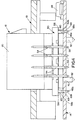
- Figure 4 specifically shows that the smaller diameter distal ends of the ground pins are inserted into the correspondingly sized ground holes 46b in printed circuit board 14, and the larger diameter proximal ends 68b of the ground pins are located within holes 60 in one of the flat flexible circuits 56.
- dual diameter terminal pins as described herein should not be limited to the disclosed use on a shield of the terminal assembly.
- the advantages of such dual-diameter pins are equally applicable for other applications whether they be signal terminal pins, ground terminal pins, stand-alone terminal pins or terminal pins which are integral parts of other structures such as the shield.
- the dual-diameter pins are specifically useful when employed as ground pins for the metal shield, because it is somewhat difficult to post-plate the distal ends of the ground pins after assembly. It is much easier to plate the pins prior to assembly of the shield onto the connector.
- Figure 4 also shows how signal pins 54 extend through holes 58 in printed circuit board 14.
- Mounting posts 52 of housing 50 also can be seen extending through mounting holes 70 in the printed circuit board.
- Figure 5 shows the proximal end 68b of one of the ground terminal pins 68 inserted through one of the holes 60 in one of the flat flexible circuits 56.
- the invention contemplates the use of a principle which may be called a "controlled meniscus".
- a particular interference is established between the ground pin and the flat flexible circuit in the curved area of the circuit around holes 60 which, in essence, is a deformed peripheral area of the flexible circuit which applies normal forces to the pin in the direction of arrows "A" when the pin is inserted into the hole in the direction of arrow "B".
- the flat flexible circuit includes a flat flexible dielectric substrate 72 preferably less than 0.050 inch thick.
- the substrate may be of various materials, but a polyimide material has proven effective. Other materials, such as a polyester material also could be used.
- a ductile flat conductor or conductive film 74 is applied to the substrate in an area at least about hole 60. The hole is preformed, such as being prepunched, in order to prevent the substrate material from tearing or "running" when the pin of a diameter larger than the diameter of the hole is inserted into the hole.
- the area and the interference forces about the hole are controlled by controlling the relative diameters of the pin and the hole. It has been found that good electrical connections can be maintained when the difference between the diameter of the pin (larger diameter proximal end 68b) and the diameter of hole 60 is on the order of 5% to 50% of the diameter of the hole. This can be termed the "interference" parameter.
- secondary operations such as soldering the pin to the flat conductor of the flat flexible circuit, or using epoxy or other adhesives between the pin and the flexible circuit can be completely eliminated and still maintain a good electrical connection between the pin and the flat conductor of the flexible circuit. This principle is quite applicable for use in an overall combination which includes the dual diameter pin, the flat flexible circuit and the printed circuit board or other connecting device as disclosed herein.
Landscapes
- Coupling Device And Connection With Printed Circuit (AREA)
- Multi-Conductor Connections (AREA)
Abstract
An electrical connector system (10) includes a flat flexible circuit (56) having
at least one pin-receiving hole (60) therein, and a printed circuit board (14) having at
least one pin-receiving hole (46b) therein aligned with the hole in the flat flexible
circuit. An electrical connector (16) includes a dielectric housing (50) and a dual-diameter
terminal pin (68) having a distal end (68a) of a smaller diameter and a
proximal end (68b) of a larger diameter. When the connector is mounted to the flat
flexible circuit (56) and the printed circuit board (14), the distal end (68a) of the pin
(68) can be inserted successively through the hole (60) in the flat flexible circuit (56)
with minimal insertion resistance and into the hole (46b) in the printed circuit board
(14), while the proximal end (68b) of the pin can be inserted into the hole (60) in the
flat flexible circuit (56) with higher insertion resistance.
Description
- This invention generally relates to the art of electrical connectors and, particularly, to an electrical connector which includes one or more terminal pins. As disclosed herein, the connector includes a shield having at least one ground pin.
- A wide variety of electrical connectors are known wherein one or more terminal pins are provided for making electrical connections to a complementary connecting device. For instance, the terminal pins may interconnect within terminal sockets of a complementary mating connector. In many applications, the terminal pins are inserted into holes in a printed circuit board, a flat flexible circuit or the like for making electrical connections to those substrate-like components. The printed circuit board typically has conductive circuit traces on the board and/or in the holes for connection, as by soldering, to the terminal pins. The flat flexible circuit typically has pin-receiving holes which are smaller in diameter than the pins, themselves, and the pins are engaged with conductive films on the flexible circuit. The terminal pins may be signal pins or ground pins, and the pins may be stand-alone components or integral components of a shield, for instance.
- In addition, it often is desirable to plate terminal pins with a highly conductive plating material to enhance the electrical connections made by the pins. There have been electrical connector applications wherein terminal pins are required to be inserted sequentially through holes in a flat flexible circuit and then into holes in a printed circuit board or other electrical device. Problems are anticipated with pins which are plated before insertion, because the plating material could tend to scrape off of the pins as they are inserted through the flat flexible circuit and before inserting into the holes in the printed circuit board or other connecting device. For instance, if the pins are plated with conductive tin material, tin "slivers" could be created which are very undesirable in the connector interface. The present invention is directed to avoiding these problems by providing an electrical connector system which employs dual-diameter pins.
- An object, therefore, of the invention is to provide a new and improved electrical connector which uses terminal pins.
- Another object of the invention is to provide a shielded electrical connector system wherein the pins are integral components of a shield of the connector.
- In the exemplary embodiment of the invention, a shielded electrical connector system is shown to include a flat flexible circuit having at least one pin-receiving hole therein. A printed circuit board has at least one pin-receiving hole therein aligned with the hole in the flat flexible circuit. An electrical connector includes a dielectric housing having a conductive shield mounted about at least a portion thereof. The shield includes at least one dual-diameter ground pin having a distal end of a smaller diameter and a proximal end of a larger diameter. Therefore, when the connector is mounted to the flat flexible circuit and the printed circuit board, the distal end of the pin can be inserted successively through the hole in the flat flexible circuit with minimal resistance and then into the hole in the printed circuit board for connection to a ground trace on the board. The larger diameter proximal end of the pin can be inserted into the hole in the flat flexible circuit with higher resistance.
- The invention is not limited to inserting the terminal pin through a flat flexible circuit and then into a hole in a printed circuit board. For instance, the pin could be inserted through the flat flexible circuit and then into a terminal socket of a different type of connecting device. In addition, the pin does not necessarily have to be an integral component of the shield.
- As disclosed herein, each of the flat flexible circuit and the printed circuit board includes a plurality of respectively aligned pin-receiving holes. The shield includes a corresponding plurality of the dual-diameter ground pins. Specifically, the conductive shield substantially surrounds the dielectric housing, and the dual-diameter ground pins are spaced generally along the periphery of the housing.
- It also is contemplated that the flat flexible circuit includes a flexible dielectric substrate less than 0.050 inch thick with a generally round pin-receiving hole of a given diameter and with a ductile conductive film on the substrate in an area at least about the hole. The diameter of the proximal end of the ground pin is greater than the hole, and the difference between the diameter of the proximal end of the ground pin and the diameter of the hole is on the order of 5% to 50% of the diameter of the hole.
- Other objects, features and advantages of the invention will be apparent from the following detailed description taken in connection with the accompanying drawings.
- The features of this invention which are believed to be novel are set forth with particularity in the appended claims. The invention, together with its objects and the advantages thereof, may be best understood by reference to the following description taken in conjunction with the accompanying drawings, in which like reference numerals identify like elements in the figures and in which:
- FIGURE 1 is an exploded perspective view of an electrical connector system in which the invention is applicable;
- FIGURE 2 is an exploded perspective view of the electrical connector assembly in the system of Figure 1 and which incorporates the terminal pins of the invention;
- FIGURE 3 is a fragmented perspective viewing showing the terminal pins of the connector assembly inserted through the flat flexible circuits;
- FIGURE 4 is a section through the connector assembly mounted in the system of Figure 1, with the die-cast housing not shown; and
- FIGURE 5 is a section through one of the holes in one of the flat flexible circuits, with the proximal end of one of the dual-diameter pins inserted into the hole.
-
- Referring to the drawings in greater detail, and first to Figure 1, the invention is embodied in an electrical connector system, generally designated 10, which includes a die-cast metal housing, generally designated 12, which receives a printed circuit board, generally designated 14, on which an electrical connector assembly, generally designated 16, is mounted. A metal cover, generally designated 18, substantially closes the assembly onto the housing, with
receptacles 20 of the connector assembly projecting through openings orapertures 22 in the cover. - More particularly,
housing 12 is recessed, as at 24, for receiving printedcircuit board 14 to whichconnector assembly 16 has been mounted. The housing has four internally threadedcorner bosses 26 for receiving appropriate fasteners (such as screws, not shown) inserted through fourmounting holes 28 at the corners ofcover 18. The housing has additionally internally threadedmounting bosses 30 for receiving appropriate fasteners extending throughnotches 32 in a pair ofend wings 34 ofconnector assembly 16. The fasteners are inserted throughholes 35 incover 18. Additional fasteners are inserted throughholes 35a in the cover and into themounting bosses 30a on the housing. Printedcircuit board 14 seats onto a plurality ofedge platform bosses 36 withinrecess 24 ofhousing 12 and onto a plurality ofcentral platform bosses 38 having projecting pin portions 38a for insertion intoappropriate mounting holes 40 in the printed circuit board. - Printed
circuit board 14 ofconnector system 10 hascorner holes 40 andcorner notches 42 aligned withcorner bosses 26 ofhousing 12 for passing therethrough of the appropriate fasteners. The printed circuit board also hasside notches 44 aligned with mountingbosses connector assembly 16. Suffice it say, the holes are arranged in a predetermined pattern or array, generally designated 46, having holes 46a corresponding to the signal terminal pins of the connector assembly andholes 46b corresponding to the ground pins of the assembly. Of course, appropriate signal and ground circuit traces are provided on the printed circuit board, as is known in the art, and which may lead to a plurality ofcircuit components 48 mounted on the board. - Referring to Figure 2 in conjunction with Figure 1,
connector assembly 16 generally is in the form of a header connector including a dielectric housing, generally designated 50, unitarily molded of plastic material or the like. The housing formsreceptacles 20 described above for insertion throughapertures 22 incover 18 ofconnector system 10. In essence,connector assembly 16 comprises a plurality (four) of separate connectors defined byreceptacles 20 within the single unitarily molded dielectric housing. Each receptacle can receive a separate complementary mating connector.Dielectric housing 50 includes a plurality of unitarily moldedmounting posts 52 for insertion into appropriate mounting holes in printedcircuit board 14 for mounting the connector assembly onto the board, as will be seen hereinafter. A plurality ofsignal terminal pins 54 are mounted inhousing 50 for each receptacle/connector 20. - Still referring to Figure 2,
connector assembly 16 includes a plurality (four) of flatflexible circuits 56, one flat flexible circuit for each receptacle/connector of the assembly. Each flat flexible circuit has an array of pin-receivingholes 58 for receivingsignal terminal pins 54. In comparing Figure 2 with Figure 1, it can be seen that external ends ofsignal terminal pins 54 can extend throughholes 58 in flatflexible circuit 56, while internal ends of the signal terminal pins are exposed withinreceptacles 20 for engaging female terminals of the complementary mating connectors. Finally, each flatflexible circuit 56 has a hole at each corner thereof for receiving ground terminal pins from a shield of the connector assembly, as described below. - In particular, an elongated, generally rectangular shield, generally designated 62, substantially surrounds
dielectric housing 50 and will be sandwiched between printedcircuit board 14 and cover 18 (Fig. 1). The shield is stamped and formed of conductive sheet metal material, such as brass or the like, which includesend wings 34 andnotches 32 described above. The shield has inwardly directedlatch tabs 64 for latchingly engagingdielectric housing 50. The shield is integrally formed with a plurality of short ground pins 66 and long ground pins 68 spaced along the opposite longitudinal sides of the elongated rectangular shield for insertion intoholes 60 in flatflexible circuits 56. At least the distal ends of the long ground pins 68 are plated with a highly conductive material such as tin or the like. - Figure 3 shows a pair of the flat
flexible circuits 56 mounted to the inside ofconnector assembly 16, with the short ground pins 66 and the long ground pins 68 ofshield 62 projecting throughholes 60 in the flat flexible circuits. Signal terminal pins 54 also can be seen projecting throughholes 58 in the circuits. - Referring to Figure 4 in conjunction with Figure 3, the invention contemplates that at least one of the ground pins on
shield 62, such as long ground pins 68, be fabricated with a dual diameter. Specifically, it can be seen that eachground pin 68 has adistal end 68a of a smaller diameter and aproximal end 68b of a larger diameter. Figure 4 specifically shows that the smaller diameter distal ends of the ground pins are inserted into the correspondingly sized ground holes 46b in printedcircuit board 14, and the larger diameter proximal ends 68b of the ground pins are located withinholes 60 in one of the flatflexible circuits 56. Therefore, it can be understood that when the connector assembly is assembled by mountinghousing 50 to flatflexible circuits 56 and printedcircuit board 14, distal ends 68a of ground pins 68 are inserted successively throughholes 60 in flatflexible circuits 56 with minimal resistance and then intoholes 46b in printedcircuit board 14 for connection to the circuit traces on the board and/or in the holes. The larger diameter proximal ends 68b of the ground pins end up located inholes 60 in the flat flexible circuits and can have higher insertion resistance therein because of the larger diameters of the proximal ends. With the distal ends of the ground pins being plated, and with the distal ends being insertable through the holes in the flat flexible circuits with minimal insertion resistance, scraping of the plating from the pins is substantially reduced if not totally eliminated. - It should be understood that the use of dual diameter terminal pins as described herein should not be limited to the disclosed use on a shield of the terminal assembly. The advantages of such dual-diameter pins are equally applicable for other applications whether they be signal terminal pins, ground terminal pins, stand-alone terminal pins or terminal pins which are integral parts of other structures such as the shield. The dual-diameter pins are specifically useful when employed as ground pins for the metal shield, because it is somewhat difficult to post-plate the distal ends of the ground pins after assembly. It is much easier to plate the pins prior to assembly of the shield onto the connector.
- Figure 4 also shows how signal pins 54 extend through
holes 58 in printedcircuit board 14. Mountingposts 52 ofhousing 50 also can be seen extending through mountingholes 70 in the printed circuit board. - Figure 5 shows the
proximal end 68b of one of the ground terminal pins 68 inserted through one of theholes 60 in one of the flatflexible circuits 56. The invention contemplates the use of a principle which may be called a "controlled meniscus". In other words, in order to eliminate the use of solder, epoxies and the like, a particular interference is established between the ground pin and the flat flexible circuit in the curved area of the circuit around holes 60 which, in essence, is a deformed peripheral area of the flexible circuit which applies normal forces to the pin in the direction of arrows "A" when the pin is inserted into the hole in the direction of arrow "B". The flat flexible circuit includes a flat flexibledielectric substrate 72 preferably less than 0.050 inch thick. The substrate may be of various materials, but a polyimide material has proven effective. Other materials, such as a polyester material also could be used. A ductile flat conductor orconductive film 74 is applied to the substrate in an area at least abouthole 60. The hole is preformed, such as being prepunched, in order to prevent the substrate material from tearing or "running" when the pin of a diameter larger than the diameter of the hole is inserted into the hole. - With the above description of the parameters of the flat flexible circuit and the pin in relation to Figure 5, the area and the interference forces about the hole are controlled by controlling the relative diameters of the pin and the hole. It has been found that good electrical connections can be maintained when the difference between the diameter of the pin (larger diameter
proximal end 68b) and the diameter ofhole 60 is on the order of 5% to 50% of the diameter of the hole. This can be termed the "interference" parameter. By maintaining these parameters, secondary operations such as soldering the pin to the flat conductor of the flat flexible circuit, or using epoxy or other adhesives between the pin and the flexible circuit can be completely eliminated and still maintain a good electrical connection between the pin and the flat conductor of the flexible circuit. This principle is quite applicable for use in an overall combination which includes the dual diameter pin, the flat flexible circuit and the printed circuit board or other connecting device as disclosed herein. - It will be understood that the invention may be embodied in other specific forms without departing from the spirit or central characteristics thereof. The present examples and embodiments, therefore, are to be considered in all respects as illustrative and not restrictive, and the invention is not to be limited to the details given herein.
Claims (11)
- A shielded electrical connector system (10), comprising:a flat flexible circuit (56) having at least one pin-receiving hole (60) therein;a printed circuit board (14) having at least one pin-receiving hole (46b) therein aligned with the hole in the flat flexible circuit;an electrical connector (16) including a dielectric housing (50); anda conductive shield (62) mounted about at least a portion of the connector housing and including a dual-diameter ground pin (68) having a distal end (68a) of a smaller diameter and a proximal end (68b) of a larger diameter whereby, when the connector (16) is mounted to the flat flexible circuit (56) and the printed circuit board (14), the distal end (68a) of the pin (68) can be inserted successively through the hole (60) in the flat flexible circuit with minimal insertion resistance and into the hole (46b) in the printed circuit board for connection to a ground trace on the board and the proximal end (68b) of the pin can be inserted into the hole (60) in the flat flexible circuit (56) with higher insertion resistance.
- The shielded electrical connector system of claim 1 wherein each of said flat flexible circuit (56) and said printed circuit board (14) includes a plurality of respectively aligned pin-receiving holes (60,46b), and said shield (62) includes a corresponding plurality of said dual-diameter ground pins (68).
- The shielded electrical connector system of claim 2 wherein said conductive shield (62) substantially surrounds the dielectric housing (50), and the dual-diameter ground pins (68) are spaced generally along the periphery of the housing.
- The shielded electrical connector system of claim 1 wherein said flat flexible circuit (56) includes a flexible dielectric substrate (72) less than 0.050 inch thick with a generally round pin-receiving hole (60) of a given diameter and with a ductile conductive film (74) on the substrate in an area at least about said hole, and the diameter of the proximal end (68b) of said ground pin (68) is greater than that of the hole (60) and wherein the difference between the diameter of the proximal end of the ground pin and the diameter of the hole is on the order of 5% to 50% of the diameter of the hole.
- An electrical connector system (10), comprising:a flat flexible circuit (56) having at least one pin-receiving hole (60) therein;a printed circuit board (14) having at least one pin-receiving hole (46b) therein aligned with the hole in the flat flexible circuit;an electrical connector (16) including a dielectric housing (50) and a dual-diameter terminal pin (68) having a distal end (68a) of a smaller diameter and a proximal end (68b) of a larger diameter whereby, when the connector (16) is mounted to the flat flexible circuit (56) and the printed circuit board (14), the distal end (68a) of the pin (68) can be inserted successively through the hole (60) in the flat flexible circuit with minimal insertion resistance and into the hole (46b) in the printed circuit board for connection to a ground trace on the board and the proximal end (68b) of the pin can be inserted into the hole (60) in the flat flexible circuit (56) with higher insertion resistance.
- The electrical connector system of claim 1 wherein each of said flat flexible circuit (56) and said printed circuit board (14) includes a plurality of respectively aligned pin-receiving holes (60,46b), and said connector (16) includes a corresponding plurality of said dual-diameter ground pins (68).
- The electrical connector system of claim 5 wherein said flat flexible circuit (56) includes a flexible dielectric substrate (72) less than 0.050 inch thick with a generally round pin-receiving hole (60) of a given diameter and with a ductile conductive film (74) on the substrate in an area at least about said hole, and the diameter of the proximal end (68b) of said ground pin (68) is greater than that of the hole (60) and wherein the difference between the diameter of the proximal end of the ground pin and the diameter of the hole is on the order of 5% to 50% of the diameter of the hole.
- A shielded electrical connector system (10), comprising:a first circuit substrate (56) having at least one pin-receiving hole (60) therein;a second circuit substrate (14) having at least one pin-receiving hole (46b) therein aligned with the hole in the first circuit substrate;an electrical connector (16) including a dielectric housing (50); anda conductive shield (62) mounted about at least a portion of the connector housing (50) and including a dual-diameter ground pin (68) having a distal end (68a) of a smaller diameter and a proximal end (68b) of a larger diameter whereby, when the connector (16) is mounted to the first circuit substrate (56) and the second circuit substrate (14), the distal end (68a) of the pin (68) can be inserted successively through the hole (60) in the first circuit substrate (56) with minimal insertion resistance and into the hole (46b) in the second circuit substrate (14) and the proximal end (68b) of the pin can be inserted into the hole in the second circuit substrate with higher insertion resistance.
- The shielded electrical connector system of claim 8 wherein each of said first and second circuit substrates (56,14) includes a plurality of respectively aligned pin-receiving holes (60,46b), and said shield (62) includes a corresponding plurality of dual-diameter ground pins (68).
- The shielded electrical connector system of claim 9 wherein said conductive shield (62) substantially surrounds the dielectric housing (50), and the dual-diameter ground pins (68) are spaced generally along the periphery of the housing.
- An electrical connector (16), comprising:a dielectric housing (50); anda conductive shield (62) mounted about at least a portion of the connector housing and including a dual-diameter ground pin (68) having a distal end (68a) of a smaller diameter and a proximal end (68b) of a larger diameter whereby, when the connector is mounted successively on a pair of connecting devices (56,14) having respective pin-receiving holes (60,46b), the distal end (68a) of the ground pin (68) can be inserted successively through a hole (60) in one of the connecting devices (56) with minimal insertion resistance and into a hole (46b) in the second connecting device (14) while the proximal end (68b) of the pin can be inserted into the hole (60) in the one connecting device (56) with higher insertion resistance.
Applications Claiming Priority (2)
| Application Number | Priority Date | Filing Date | Title |
|---|---|---|---|
| US262767 | 1988-10-26 | ||
| US26276799A | 1999-03-04 | 1999-03-04 |
Publications (1)
| Publication Number | Publication Date |
|---|---|
| EP1033787A1 true EP1033787A1 (en) | 2000-09-06 |
Family
ID=22998951
Family Applications (1)
| Application Number | Title | Priority Date | Filing Date |
|---|---|---|---|
| EP00104302A Withdrawn EP1033787A1 (en) | 1999-03-04 | 2000-03-02 | Electrical connector with terminal pins |
Country Status (1)
| Country | Link |
|---|---|
| EP (1) | EP1033787A1 (en) |
Cited By (7)
| Publication number | Priority date | Publication date | Assignee | Title |
|---|---|---|---|---|
| EP1286419A3 (en) * | 2001-08-21 | 2003-12-10 | Lumberg Automation Components GmbH & Co. KG | Electrical connector |
| EP1548887A1 (en) * | 2003-11-27 | 2005-06-29 | Yazaki Corporation | Connector with integrated board |
| US7445455B2 (en) | 2004-09-29 | 2008-11-04 | Hitachi, Ltd. | Electronic device |
| US7537461B2 (en) | 2003-07-16 | 2009-05-26 | Gryphics, Inc. | Fine pitch electrical interconnect assembly |
| WO2008122005A3 (en) * | 2007-04-02 | 2009-10-08 | Gryphics, Inc. | Fine pitch electrical interconnect assembly |
| EP2760086A1 (en) * | 2013-01-29 | 2014-07-30 | AVX Corporation | Modular electrical connector assembly and associated method of making |
| EP4486085A1 (en) * | 2023-06-27 | 2025-01-01 | Hamilton Sundstrand Corporation | Integrated scalable connector pin field emi shielding assembly and a method for implementing same |
Citations (3)
| Publication number | Priority date | Publication date | Assignee | Title |
|---|---|---|---|---|
| US4797113A (en) * | 1987-02-05 | 1989-01-10 | Lambert Roger T | Board to board flexible pin |
| US5384435A (en) * | 1994-01-28 | 1995-01-24 | Molex Incorporated | Mounting terminal pins in substrates |
| WO1997045898A1 (en) * | 1996-05-31 | 1997-12-04 | The Whitaker Corporation | Shield member for panel mount connector |
-
2000
- 2000-03-02 EP EP00104302A patent/EP1033787A1/en not_active Withdrawn
Patent Citations (3)
| Publication number | Priority date | Publication date | Assignee | Title |
|---|---|---|---|---|
| US4797113A (en) * | 1987-02-05 | 1989-01-10 | Lambert Roger T | Board to board flexible pin |
| US5384435A (en) * | 1994-01-28 | 1995-01-24 | Molex Incorporated | Mounting terminal pins in substrates |
| WO1997045898A1 (en) * | 1996-05-31 | 1997-12-04 | The Whitaker Corporation | Shield member for panel mount connector |
Cited By (13)
| Publication number | Priority date | Publication date | Assignee | Title |
|---|---|---|---|---|
| EP1286419A3 (en) * | 2001-08-21 | 2003-12-10 | Lumberg Automation Components GmbH & Co. KG | Electrical connector |
| US7537461B2 (en) | 2003-07-16 | 2009-05-26 | Gryphics, Inc. | Fine pitch electrical interconnect assembly |
| EP1548887A1 (en) * | 2003-11-27 | 2005-06-29 | Yazaki Corporation | Connector with integrated board |
| US7125285B2 (en) | 2003-11-27 | 2006-10-24 | Yazaki Corporation | Joint connector |
| EP1643820B1 (en) * | 2004-09-29 | 2010-12-22 | Hitachi, Ltd. | Electronic device having a heat resistant circuit board and a connector |
| US7445455B2 (en) | 2004-09-29 | 2008-11-04 | Hitachi, Ltd. | Electronic device |
| WO2008122005A3 (en) * | 2007-04-02 | 2009-10-08 | Gryphics, Inc. | Fine pitch electrical interconnect assembly |
| EP2760086A1 (en) * | 2013-01-29 | 2014-07-30 | AVX Corporation | Modular electrical connector assembly and associated method of making |
| US9048560B2 (en) | 2013-01-29 | 2015-06-02 | Avx Corporation | Modular electrical connector assembly and associated method of making |
| US9362694B2 (en) | 2013-01-29 | 2016-06-07 | Avx Corporation | Modular electrical connector assembly and associated method of making |
| US9705234B2 (en) | 2013-01-29 | 2017-07-11 | Avx Corporation | Modular electrical connector assembly and associated method of making |
| US10348029B2 (en) | 2013-01-29 | 2019-07-09 | Avx Corporation | Modular electrical connector assembly and associated method of making |
| EP4486085A1 (en) * | 2023-06-27 | 2025-01-01 | Hamilton Sundstrand Corporation | Integrated scalable connector pin field emi shielding assembly and a method for implementing same |
Similar Documents
| Publication | Publication Date | Title |
|---|---|---|
| JP3646894B2 (en) | Electric connector shroud and electric connector assembly using the same | |
| US6206728B1 (en) | Shielded electrical connector system | |
| JP2724657B2 (en) | Low profile electrical connector | |
| US5624277A (en) | Filtered and shielded electrical connector using resilient electrically conductive member | |
| US6315620B1 (en) | System, method, and device for a pre-loaded straddle mounted connector assembly | |
| US5498167A (en) | Board to board electrical connectors | |
| US5613860A (en) | Universal grounding clip for card-receiving connector | |
| EP0347097A1 (en) | Electrical connector system | |
| US6083046A (en) | Receptacle connector | |
| EP0676833A2 (en) | Surface mountable card edge connector | |
| US5967831A (en) | Electrical connector assembly | |
| WO2010019332A2 (en) | Electrical connector assembly | |
| JP3092060B2 (en) | Printed circuit board mounted electrical connector with multifunctional board lock | |
| EP0624928A1 (en) | Shielded electrical connector assembly | |
| EP1516400A1 (en) | Electrical connector with wire management module | |
| JP2007525808A (en) | Connector device | |
| US5281155A (en) | Electrical connector with electrostatic discharge protection | |
| US7264507B2 (en) | Screen connector device for a circuit board mounted within a housing | |
| US6790052B2 (en) | Circuit board straddle mounted connector | |
| WO2021016454A1 (en) | Safe, robust, compact connector | |
| JPH0247071B2 (en) | ||
| US6132247A (en) | Metallic one-piece hold-down and an electrical connector with the hold-down | |
| US5562499A (en) | Multiposition electrical connector filter adapter | |
| EP0643448A1 (en) | Coaxial connector for connection to a printed circuit board | |
| US5967806A (en) | Electrical connector arrangement |
Legal Events
| Date | Code | Title | Description |
|---|---|---|---|
| PUAI | Public reference made under article 153(3) epc to a published international application that has entered the european phase |
Free format text: ORIGINAL CODE: 0009012 |
|
| AK | Designated contracting states |
Kind code of ref document: A1 Designated state(s): DE FR GB IT |
|
| AX | Request for extension of the european patent |
Free format text: AL;LT;LV;MK;RO;SI |
|
| 17P | Request for examination filed |
Effective date: 20010228 |
|
| AKX | Designation fees paid |
Free format text: DE FR GB IT |
|
| STAA | Information on the status of an ep patent application or granted ep patent |
Free format text: STATUS: THE APPLICATION IS DEEMED TO BE WITHDRAWN |
|
| 18D | Application deemed to be withdrawn |
Effective date: 20021001 |