EP0676833A2 - Surface mountable card edge connector - Google Patents
Surface mountable card edge connector Download PDFInfo
- Publication number
- EP0676833A2 EP0676833A2 EP95301365A EP95301365A EP0676833A2 EP 0676833 A2 EP0676833 A2 EP 0676833A2 EP 95301365 A EP95301365 A EP 95301365A EP 95301365 A EP95301365 A EP 95301365A EP 0676833 A2 EP0676833 A2 EP 0676833A2
- Authority
- EP
- European Patent Office
- Prior art keywords
- termini
- connector
- board
- row
- housing
- Prior art date
- Legal status (The legal status is an assumption and is not a legal conclusion. Google has not performed a legal analysis and makes no representation as to the accuracy of the status listed.)
- Granted
Links
Images

Classifications
-
- H—ELECTRICITY
- H01—ELECTRIC ELEMENTS
- H01R—ELECTRICALLY-CONDUCTIVE CONNECTIONS; STRUCTURAL ASSOCIATIONS OF A PLURALITY OF MUTUALLY-INSULATED ELECTRICAL CONNECTING ELEMENTS; COUPLING DEVICES; CURRENT COLLECTORS
- H01R12/00—Structural associations of a plurality of mutually-insulated electrical connecting elements, specially adapted for printed circuits, e.g. printed circuit boards [PCB], flat or ribbon cables, or like generally planar structures, e.g. terminal strips, terminal blocks; Coupling devices specially adapted for printed circuits, flat or ribbon cables, or like generally planar structures; Terminals specially adapted for contact with, or insertion into, printed circuits, flat or ribbon cables, or like generally planar structures
- H01R12/50—Fixed connections
- H01R12/51—Fixed connections for rigid printed circuits or like structures
- H01R12/55—Fixed connections for rigid printed circuits or like structures characterised by the terminals
- H01R12/57—Fixed connections for rigid printed circuits or like structures characterised by the terminals surface mounting terminals
-
- H—ELECTRICITY
- H01—ELECTRIC ELEMENTS
- H01R—ELECTRICALLY-CONDUCTIVE CONNECTIONS; STRUCTURAL ASSOCIATIONS OF A PLURALITY OF MUTUALLY-INSULATED ELECTRICAL CONNECTING ELEMENTS; COUPLING DEVICES; CURRENT COLLECTORS
- H01R12/00—Structural associations of a plurality of mutually-insulated electrical connecting elements, specially adapted for printed circuits, e.g. printed circuit boards [PCB], flat or ribbon cables, or like generally planar structures, e.g. terminal strips, terminal blocks; Coupling devices specially adapted for printed circuits, flat or ribbon cables, or like generally planar structures; Terminals specially adapted for contact with, or insertion into, printed circuits, flat or ribbon cables, or like generally planar structures
- H01R12/70—Coupling devices
- H01R12/71—Coupling devices for rigid printing circuits or like structures
- H01R12/72—Coupling devices for rigid printing circuits or like structures coupling with the edge of the rigid printed circuits or like structures
- H01R12/721—Coupling devices for rigid printing circuits or like structures coupling with the edge of the rigid printed circuits or like structures cooperating directly with the edge of the rigid printed circuits
-
- H—ELECTRICITY
- H01—ELECTRIC ELEMENTS
- H01R—ELECTRICALLY-CONDUCTIVE CONNECTIONS; STRUCTURAL ASSOCIATIONS OF A PLURALITY OF MUTUALLY-INSULATED ELECTRICAL CONNECTING ELEMENTS; COUPLING DEVICES; CURRENT COLLECTORS
- H01R4/00—Electrically-conductive connections between two or more conductive members in direct contact, i.e. touching one another; Means for effecting or maintaining such contact; Electrically-conductive connections having two or more spaced connecting locations for conductors and using contact members penetrating insulation
- H01R4/02—Soldered or welded connections
- H01R4/028—Soldered or welded connections comprising means for preventing flowing or wicking of solder or flux in parts not desired
Definitions
- the present invention is related to surface mountable electrical connectors and more particularly to high density connectors.
- the electronic industry today requires high-speed electronic equipment that is relatively compact and densely packaged. Typically the equipment includes one or more mother and daughter board assemblies. To reduce board space and eliminate the need for throughholes it is desirable to provide electrical connectors and devices that can be mounted to circuit pads on the surfaces of the circuit boards. It is also desirable to provide high-speed card edge connectors having a controlled impedance that will essentially match the impedance of the circuit board.
- a high-speed card edge connector is one that can pass fast rise time signals without distorting or degrading that rise time. It is desirable, therefore, to control the impedance of the connector to reduce signal reflection caused by changes in the impedance in the pathways conducting the digital pulse. Impedance control also requires close spacing of ground and signal traces in interconnections.
- U.S. Patents 5,026,292 and 5,051,099 disclose high-speed card edge connectors having closely spaced ground contact members and signal contact members, each pair of signal contact members having associated ground contact member.
- the contact members in these patents have soldered tails that engage throughholes in a mother board.
- the solder tails and the throughholes are arranged in staggered arrays.
- the solder tail portions of adjacent signal and ground contact members have different configurations requiring four different signal contact members and two different ground contact members, which greatly increases the cost of manufacturing the connector.
- the present invention is directed to an electrical connector that is surface mountable and provides a means for interconnecting a dense array of electrical terminal members to a circuit board of the type having an outer row of trace termini and inner row of trace termini closely spaced therefrom on the mounting surface of the board.
- the invention will be described in terms of a high-speed card edge connector. It is to be understood, however, that the invention is not limited to the connector described herein.
- the electrical connector includes a dielectric housing having a mounting face and a mating face and at least one row of electrical terminal members extending therebetween.
- the terminal members are arranged adjacent to each other in a dense array, the terminal members including an elongate arm portion extending from the mounting face of the housing to surface mount contact sections at the free ends thereof associated with one of the trace terminus of the circuit board.
- Each of the terminal members associated with an outer row of termini include a portion immediately adjacent to the surface mount contact section that is abruptly directed away from the mounting surface of the circuit board at least a selected distance above the spacing between the outer and inner rows of circuit board termini. The spacing minimizes wicking of solder at the termini thereby preventing solder from wicking from the elongate arm to closely adjacent ones of the termini of the inner row.
- other terminal members associated with inner row of termini on the circuit board include a registration section on the elongate arm portion.
- the registration section is retained in a recess extending into the housing from the mounting face thereof adjacent the outer sidewalls and proximate the free ends of the terminal members.
- the registration section holds the free ends of the other terminal members in a registered spacing during the handling and mounting of the connector to the circuit board thereby preventing inadvertent engagement with closely spaced adjacent terminal members.
- the terminal members that engage the outer row of surface termini on the circuit board connect signal lines and the terminal members that engage the inner row of termini are connected to ground.
- An advantage of the invention is to provide a surface mountable connector designed to minimize the risk of solder being wicked to closely adjacent termini on the surface of the circuit board.
- An additional advantage of the invention is to provide a means for controlling the registered spacing of terminal members in a connector during the handling and mounting of the connector to the board.
- a further advantage of the invention is to provide a surface mountable connector having one or more rows of terminal members wherein soldered connections between contact surfaces at the free ends of the terminals and termini on the circuit board are accessible for reworking, i.e. soldering of a single connection using a soldering gun or the like, if necessary.
- Another advantage of the present invention is to provide a surface mountable one-piece grounded high-speed connector.
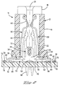
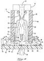
- FIG. 1 shows an electrical connector 10 comprising a dielectric housing member 12 having a plurality of first and second terminal members 30,46 having respective surface mounted sections 38,54 to be mounted to respective termini 76,84 of circuit board 70.
- Dielectric housing member 12 has opposed sidewalls 14, endwalls 16, mounting face 18 and mating face 24.
- the connector shown is known as a high-speed card edge connector having alternating signal and ground terminal members and includes a card receiving slot 26.
- Housing 12 further includes a plurality of terminal receiving cavities 28 for receiving respective first and second terminal members 30,46 respectively.
- the first terminal members 30 are signal terminal members and the second terminal members 46 are ground terminal members.
- Housing 12 further includes an inner wall 22 on which is mounted ground contact 46.
- Circuit board 70 includes a mounting surface 72 having a pair of outer rows 74, a pair of inner rows 82, and a center row 88 of surface termini 76,84,90 respectively.
- the outer row 74 of termini 76 are signal termini and the inner rows 82 of termini 84 are ground termini.
- circuit board 70 further includes a center row 88 of ground termini 90.
- Circuit board 70 also includes mounting aperture 94 for securing a board lock such as 66 and alignment posts or the like (not shown) when connector 10 is mounted to the circuit board 70.
- the signal terminal members 30 include a body section 32 having a first contact portion 34 and a second contact portion 42.
- Terminal body 32 further includes means (not shown) for securing the terminal member 30 in housing 12.
- the first contact portion 34 of each terminal member 30 includes an elongate arm portion 36 extending outwardly from the mounting face 18 of the housing 12 to a surface mount contact section 38 at the free end thereof.
- Each surface mount contact section 38 is associated with a respective one of the signal trace termini 76 in outer row 74 of the circuit board 70.
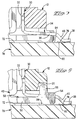
- Each elongate arm portion 36 includes a portion 40 immediately adjacent the surface mount contact section 38 that is abruptly directed away from the mounting surface 72 of circuit board 70, as best seen in Figures 2 and 3, thus raising the remaining portion of arm 36 at least a selected distance above the spacing 80 between the inner and outer rows 74,82 of termini 76,84.
- Figure 2 shows contact sections 38 electrically connected by solder 78 to respective termini 76.
- solder 78 has been eliminated from Figure 3.
- the abrupt portion 40 of the elongate arm 36 raises arm 36 a sufficient distance above the inner termini row 82 thereby preventing the solder from wicking to the closely adjacent inner row 82 of termini 84.
- the second terminal member 46 in the high-speed card edge connector 10 is a ground contact member having a body 48 secured to a wall 22 within housing 12 as described in U.S. Patents 5,026,292 and 5,051,099.
- Terminal body 48 includes a first contact section 50 for engaging the circuit board 70 and a second contact section 60.
- the first contact section 50 includes an elongate arm 52 having a surface mount portion 54 at the free end thereof and a registration portion 56 extending in a direction opposite to the circuit board 70. Registration portion or tab 56 is engaged in retention slot 20 of housing 12.
- the body 48 of ground terminal member 46 includes a pair of first contact sections 50 having respective elongate arms 52 extending in opposite directions to free ends, each having a surface mount contact section 54 for engaging a respective second termini 84 in the respective second termini rows 82.
- Registration portions 56 assure that the free ends 54 of the elongate arms 52 are retained in a registered spacing during the handling and mounting of connector 10 to board 70 thereby preventing inadvertent engagement with closely adjacent signal contacts.
- body 48 of ground terminal member 46 further includes a middle contact or foot section 58 for engaging the surface mount termini 90 in center termini row 88 of circuit board 70.
- the middle contact or foot 58 also provides support for the continuously extending elongate arms 52 as well as provides a potential third interconnection site for the ground terminal member 46.
- Figure 4 shows contact sections 54,58 electrically connected by solder 86,92 to respective termini 84,90. For purposes of clarity, solder 86 has been eliminated from Figure 5.
- the registration portions 56 which are received in housing recess or slots 20 maintain the continuously extending ground contact sections 50 in a true position along the mounting face 18 of the housing 12 thereby assuring that the three contact surfaces 54 at the free ends thereof and 58 at the center engage the respective termini 84,90,84 respectively.
- both of the contact surfaces 54 be soldered to their respective termini 84 on the board 70. It is to be recognized, however, that a minimum of one of the three surfaces 54,58,54 actually needs to be connected to the ground within the circuit board to effect grounding.
- the center surface 58 need not be electrically connected to a termini 90 on the board 70, it is desirable, however, to have support at the center of the terminal member 46 to prevent stress being applied to solder fillets 86 at the outer edges 54 of the connector 10 when a card (not shown) is inserted into the card receiving slot 26 of connector 10.
- solder paste is typically screened onto the various termini 76,84,90.
- the free ends 38,54 of the terminal members 30,46 are aligned with their respective termini as the connector 10 is mounted to the board and secured thereto with holding means such as 66 and use of other alignment means such as pylons (not shown) and the like as known in the art.
- the assembly of connector 10 and board 70 are heated such as for example in an infrared oven to reflow the solder fillets 78,86, and 92 and electrically connect and secure the respective surface mount contact sections 38, 54,and 58 to their respective termini 76,84, and 90, as shown in Figures 2 and 4.
- the enlarged surface mount free end 54 of the ground terminal members 46 provides access to the free end 54 to permit reworking of the solder connection should it become necessary.
- housing 12 is formed from a dielectric material such as for example, liquid crystal polymers, or polyphenylene sulfide, which are readily available from a number of commercial sources. Other suitable materials capable of withstanding the soldering temperatures associated with surface mount technology, as known in the art, may also be used. It should be recognized that the terminal members 30,46 of connector 10 may also be electrically connected to the respective circuit board termini 76,84 by means of conductive adhesive or other materials as known in the art.
- the dielectric material selected for the housing therefore, would be one that is compatable with the conductive material selected and method used to interconnect the conductors to the board termini.
- the signal terminal members 30 and ground terminal members 46 are stamped and formed from phosphor bronze or other materials having the desired spring characteristics to provide sufficient normal force.
- the abrupt change in the elongate arm 36 of the signal terminal member provides a means to surface mount a close array of terminal members to a board having a densely spaced array of inner and outer termini.
- the invention also provides for a means for maintaining the true position of a continuously extending ground contact or other terminal member.
- the present invention further provides the advantage of having only two different signal terminal members 30, one for the right hand row of the connector and the other for the left hand row of the housing and only one ground terminal member 46.
- the reduction in the number of different terminal members as compared to the ones used in the connectors of the prior art patents provides a more cost effective means of manufacturing the high-speed connector.
- the present invention allows for a closely spaced array of terminal members to be mounted to a surface of a circuit board thereby eliminating the need to provide a plurality of through holes in the board.
Abstract
Description
- The present invention is related to surface mountable electrical connectors and more particularly to high density connectors.
- The electronic industry today requires high-speed electronic equipment that is relatively compact and densely packaged. Typically the equipment includes one or more mother and daughter board assemblies. To reduce board space and eliminate the need for throughholes it is desirable to provide electrical connectors and devices that can be mounted to circuit pads on the surfaces of the circuit boards. It is also desirable to provide high-speed card edge connectors having a controlled impedance that will essentially match the impedance of the circuit board. A high-speed card edge connector is one that can pass fast rise time signals without distorting or degrading that rise time. It is desirable, therefore, to control the impedance of the connector to reduce signal reflection caused by changes in the impedance in the pathways conducting the digital pulse. Impedance control also requires close spacing of ground and signal traces in interconnections. With the close spacing of the ground and signal terminal members within the housing and conductive traces within the board, it is also necessary to prevent cross-talk between the adjacent interconnections. U.S. Patents 5,026,292 and 5,051,099 disclose high-speed card edge connectors having closely spaced ground contact members and signal contact members, each pair of signal contact members having associated ground contact member. The contact members in these patents have soldered tails that engage throughholes in a mother board. In order to accommodate the dense array of solder tails for the signal and ground contact members, the solder tails and the throughholes are arranged in staggered arrays. In the embodiments shown, the solder tail portions of adjacent signal and ground contact members have different configurations requiring four different signal contact members and two different ground contact members, which greatly increases the cost of manufacturing the connector.
- The present invention is directed to an electrical connector that is surface mountable and provides a means for interconnecting a dense array of electrical terminal members to a circuit board of the type having an outer row of trace termini and inner row of trace termini closely spaced therefrom on the mounting surface of the board. For purposes of illustration, the invention will be described in terms of a high-speed card edge connector. It is to be understood, however, that the invention is not limited to the connector described herein.
- In accordance with the present invention the electrical connector includes a dielectric housing having a mounting face and a mating face and at least one row of electrical terminal members extending therebetween. The terminal members are arranged adjacent to each other in a dense array, the terminal members including an elongate arm portion extending from the mounting face of the housing to surface mount contact sections at the free ends thereof associated with one of the trace terminus of the circuit board. Each of the terminal members associated with an outer row of termini include a portion immediately adjacent to the surface mount contact section that is abruptly directed away from the mounting surface of the circuit board at least a selected distance above the spacing between the outer and inner rows of circuit board termini. The spacing minimizes wicking of solder at the termini thereby preventing solder from wicking from the elongate arm to closely adjacent ones of the termini of the inner row.
- In the embodiment shown, other terminal members associated with inner row of termini on the circuit board include a registration section on the elongate arm portion. The registration section is retained in a recess extending into the housing from the mounting face thereof adjacent the outer sidewalls and proximate the free ends of the terminal members. The registration section holds the free ends of the other terminal members in a registered spacing during the handling and mounting of the connector to the circuit board thereby preventing inadvertent engagement with closely spaced adjacent terminal members. In the embodiment shown the terminal members that engage the outer row of surface termini on the circuit board connect signal lines and the terminal members that engage the inner row of termini are connected to ground.
- An advantage of the invention is to provide a surface mountable connector designed to minimize the risk of solder being wicked to closely adjacent termini on the surface of the circuit board.
- An additional advantage of the invention is to provide a means for controlling the registered spacing of terminal members in a connector during the handling and mounting of the connector to the board.
- A further advantage of the invention is to provide a surface mountable connector having one or more rows of terminal members wherein soldered connections between contact surfaces at the free ends of the terminals and termini on the circuit board are accessible for reworking, i.e. soldering of a single connection using a soldering gun or the like, if necessary.
- Another advantage of the present invention is to provide a surface mountable one-piece grounded high-speed connector.
- An embodiment of the present invention will now be described by way of example with reference to the accompanying drawings in which:
- Figure 1 is an exploded fragmentary perspective view of the connector of the invention exploded from the circuit board.
- Figure 2 is a cross-sectional view of the connector of Figure 1 mounted to the circuit board and showing the array of terminal members soldered to the outer termini of the circuit board.
- Figure 3 is an enlarged fragmentary view of a portion of Figure 2 illustrating the position of the terminal members to the outer termini.
- Figure 4 is a cross-sectional view of the connector of Figure 1 mounted to the circuit board and illustrating the terminal members connected to the inner row of termini of the circuit board.
- Figure 5 is an enlarged fragmentary section of Figure 4 illustrating the position of the terminal members to the inner row of termini.
- Figure 1 shows an
electrical connector 10 comprising adielectric housing member 12 having a plurality of first andsecond terminal members sections respective termini circuit board 70.Dielectric housing member 12 has opposedsidewalls 14,endwalls 16, mountingface 18 andmating face 24. For purposes of illustrating the invention the connector shown is known as a high-speed card edge connector having alternating signal and ground terminal members and includes acard receiving slot 26.Housing 12 further includes a plurality ofterminal receiving cavities 28 for receiving respective first andsecond terminal members first terminal members 30 are signal terminal members and thesecond terminal members 46 are ground terminal members.Housing 12 further includes aninner wall 22 on which is mountedground contact 46. -
Circuit board 70 includes amounting surface 72 having a pair ofouter rows 74, a pair ofinner rows 82, and acenter row 88 ofsurface termini outer row 74 oftermini 76 are signal termini and theinner rows 82 oftermini 84 are ground termini. In the preferredembodiment circuit board 70 further includes acenter row 88 ofground termini 90.Circuit board 70 also includesmounting aperture 94 for securing a board lock such as 66 and alignment posts or the like (not shown) whenconnector 10 is mounted to thecircuit board 70. - Referring now to Figures 1, 2 and 3, the
signal terminal members 30 include abody section 32 having afirst contact portion 34 and asecond contact portion 42.Terminal body 32 further includes means (not shown) for securing theterminal member 30 inhousing 12. Thefirst contact portion 34 of eachterminal member 30 includes anelongate arm portion 36 extending outwardly from themounting face 18 of thehousing 12 to a surfacemount contact section 38 at the free end thereof. Each surfacemount contact section 38 is associated with a respective one of thesignal trace termini 76 inouter row 74 of thecircuit board 70. Eachelongate arm portion 36 includes aportion 40 immediately adjacent the surfacemount contact section 38 that is abruptly directed away from themounting surface 72 ofcircuit board 70, as best seen in Figures 2 and 3, thus raising the remaining portion ofarm 36 at least a selected distance above thespacing 80 between the inner andouter rows termini contact sections 38 electrically connected bysolder 78 torespective termini 76. For purposes of clarity,solder 78 has been eliminated from Figure 3. As can be seen in Figure 3 it is critical that thespacing 80 between the first andsecond rows termini abrupt portion 40 of theelongate arm 36 raises arm 36 a sufficient distance above theinner termini row 82 thereby preventing the solder from wicking to the closely adjacentinner row 82 oftermini 84. - Referring now to Figures 1, 4 and 5, the
second terminal member 46 in the high-speedcard edge connector 10 is a ground contact member having abody 48 secured to awall 22 withinhousing 12 as described in U.S. Patents 5,026,292 and 5,051,099.Terminal body 48 includes afirst contact section 50 for engaging thecircuit board 70 and asecond contact section 60. Thefirst contact section 50 includes anelongate arm 52 having asurface mount portion 54 at the free end thereof and aregistration portion 56 extending in a direction opposite to thecircuit board 70. Registration portion ortab 56 is engaged inretention slot 20 ofhousing 12. In the preferred embodiment thebody 48 ofground terminal member 46 includes a pair offirst contact sections 50 having respectiveelongate arms 52 extending in opposite directions to free ends, each having a surfacemount contact section 54 for engaging a respectivesecond termini 84 in the respectivesecond termini rows 82.Registration portions 56 assure that thefree ends 54 of theelongate arms 52 are retained in a registered spacing during the handling and mounting ofconnector 10 toboard 70 thereby preventing inadvertent engagement with closely adjacent signal contacts. In the preferredembodiment body 48 ofground terminal member 46 further includes a middle contact orfoot section 58 for engaging thesurface mount termini 90 incenter termini row 88 ofcircuit board 70. The middle contact orfoot 58 also provides support for the continuously extendingelongate arms 52 as well as provides a potential third interconnection site for theground terminal member 46. Figure 4 showscontact sections solder respective termini solder 86 has been eliminated from Figure 5. - As can best be seen in Figure 4, the
registration portions 56 which are received in housing recess orslots 20 maintain the continuously extendingground contact sections 50 in a true position along themounting face 18 of thehousing 12 thereby assuring that the threecontact surfaces 54 at the free ends thereof and 58 at the center engage therespective termini contact surfaces 54 be soldered to theirrespective termini 84 on theboard 70. It is to be recognized, however, that a minimum of one of the threesurfaces center surface 58 need not be electrically connected to a termini 90 on theboard 70, it is desirable, however, to have support at the center of theterminal member 46 to prevent stress being applied tosolder fillets 86 at theouter edges 54 of theconnector 10 when a card (not shown) is inserted into thecard receiving slot 26 ofconnector 10. - In mounting the
connector 10 toboard 70, solder paste is typically screened onto thevarious termini terminal members connector 10 is mounted to the board and secured thereto with holding means such as 66 and use of other alignment means such as pylons (not shown) and the like as known in the art. After mounting, the assembly ofconnector 10 andboard 70 are heated such as for example in an infrared oven to reflow thesolder fillets mount contact sections respective termini free end 54 of theground terminal members 46 provides access to thefree end 54 to permit reworking of the solder connection should it become necessary. - In making the
electrical connector 10 in accordance with theinvention housing 12 is formed from a dielectric material such as for example, liquid crystal polymers, or polyphenylene sulfide, which are readily available from a number of commercial sources. Other suitable materials capable of withstanding the soldering temperatures associated with surface mount technology, as known in the art, may also be used. It should be recognized that theterminal members connector 10 may also be electrically connected to the respective circuit board termini 76,84 by means of conductive adhesive or other materials as known in the art. The dielectric material selected for the housing, therefore, would be one that is compatable with the conductive material selected and method used to interconnect the conductors to the board termini. - The
signal terminal members 30 andground terminal members 46 are stamped and formed from phosphor bronze or other materials having the desired spring characteristics to provide sufficient normal force. - As can be seen from the foregoing description, the abrupt change in the
elongate arm 36 of the signal terminal member provides a means to surface mount a close array of terminal members to a board having a densely spaced array of inner and outer termini. The invention also provides for a means for maintaining the true position of a continuously extending ground contact or other terminal member. - In the embodiment shown, the present invention further provides the advantage of having only two different
signal terminal members 30, one for the right hand row of the connector and the other for the left hand row of the housing and only oneground terminal member 46. The reduction in the number of different terminal members as compared to the ones used in the connectors of the prior art patents provides a more cost effective means of manufacturing the high-speed connector. The present invention allows for a closely spaced array of terminal members to be mounted to a surface of a circuit board thereby eliminating the need to provide a plurality of through holes in the board.
Claims (5)
- A surface mountable electrical connector (10) for use with a circuit board (70) having an outer row (74) of trace termini (76) and an inner row (82) of trace termini (84) closely spaced therefrom on the mounting surface (72) of said board (70), said connector (10) including a dielectric housing (12) having at least one row of electrical terminal members (30) extending therebetween, said terminal members (30) being arranged adjacent to each other and in a dense array in said at least one row, said terminal members (30) including elongate arm portions extending from said housing (12) to surface mount contact sections (38) at free ends thereof associated with a respective one of said trace termini (76,84) of said circuit board (70), the connector (10) being characterized in that:
each said terminal member (30) associated with said outer row (74) of termini includes a portion (40) immediately adjacent said surface mount contact section (38) that is abruptly directed away from said mounting surface (72)of said circuit board (70) at least a selected distance above the spacing between said outer and inner rows (74,82) of said termini (76,84) to minimize wicking of solder thereat thereby preventing solder from wicking to closely adjacent ones of said termini (84) of said inner row. - A surface mountable electrical connector (10) for use with a circuit board (70) having at least one row (82) of trace termini (84) on the mounting surface (72) of said board (70), said connector (10) including a dielectric housing (12) having at least one row of electrical terminal members (46) therein, said terminal members (46) being arranged adjacent to each other and in a dense array in said at least one row, said terminal members (46) including elongate arm portions (52) extending from said housing (12) to surface mount contact sections (54) at free ends thereof associated with a respective one of said trace termini (84) of said circuit board (70) the connector (10) being characterized in that:
each said terminal member (46) has a registration portion (56) proximate a said free end thereof and directed upwardly away from the mounting surface (72) of the board (70) said registration portion (56) being receivable in an associated recess (20) extending into said housing (12), at the mounting face (18) thereof, thereby maintaining the registration of said elongate arm portions (52) and the accurate spacing of said surface mount contact sections (54) during handling and mounting of said connector (10) to said board (70) and preventing inadvertent engagement with closely spaced contact sections and misalignment with corresponding trace termini (84). - The surface mountable electrical connector of claim 2 wherein said terminal member (46) is a ground terminal member, said ground terminal member including two elongate arm portions (52) extending in opposite directions from said housing (12), each having a respective registration portion (54).
- The surface mountable electrical connector (10) of claim 3 wherein each said ground terminal member (46) includes a board support section (58) intermediate said two elongate arm portions (52).
- The surface mountable electrical connector (10) of claim 4 wherein said board support section (58) is electrically connectable to ground termini (90) on said board (70).
Applications Claiming Priority (2)
| Application Number | Priority Date | Filing Date | Title |
|---|---|---|---|
| US223895 | 1994-04-06 | ||
| US08/223,895 US5496180A (en) | 1994-04-06 | 1994-04-06 | Surface mountable card edge connector |
Publications (3)
| Publication Number | Publication Date |
|---|---|
| EP0676833A2 true EP0676833A2 (en) | 1995-10-11 |
| EP0676833A3 EP0676833A3 (en) | 1996-04-03 |
| EP0676833B1 EP0676833B1 (en) | 2001-05-16 |
Family
ID=22838412
Family Applications (1)
| Application Number | Title | Priority Date | Filing Date |
|---|---|---|---|
| EP95301365A Expired - Lifetime EP0676833B1 (en) | 1994-04-06 | 1995-03-03 | Surface mountable card edge connector |
Country Status (6)
| Country | Link |
|---|---|
| US (1) | US5496180A (en) |
| EP (1) | EP0676833B1 (en) |
| JP (1) | JPH08124637A (en) |
| KR (1) | KR100344866B1 (en) |
| DE (1) | DE69520905T2 (en) |
| MY (1) | MY115346A (en) |
Cited By (16)
| Publication number | Priority date | Publication date | Assignee | Title |
|---|---|---|---|---|
| WO1996038889A1 (en) * | 1995-05-31 | 1996-12-05 | Teradyne, Inc. | Surface mounted electrical connector |
| EP0774808A1 (en) * | 1995-11-16 | 1997-05-21 | Molex Incorporated | Right-angle board to board connector with anti-wicking characteristics and terminal for same |
| FR2752098A1 (en) * | 1996-08-02 | 1998-02-06 | Framatome Connectors Int | PCB to pcb connector assembly for high speed signals |
| EP0877448A2 (en) * | 1997-05-08 | 1998-11-11 | Framatome Connectors International | High speed card edge connector with four bladed ground contact |
| EP0913892A2 (en) * | 1997-11-03 | 1999-05-06 | Molex Incorporated | Laminated spring structure and flexible circuitry connector incorporating same |
| US5904581A (en) * | 1996-07-17 | 1999-05-18 | Minnesota Mining And Manufacturing Company | Electrical interconnection system and device |
| EP0926779A1 (en) * | 1997-12-23 | 1999-06-30 | Berg Electronics Manufacturing B.V. | High density edge card connector and method of making the same |
| WO1999041810A1 (en) * | 1998-02-17 | 1999-08-19 | Rambus, Inc. | Connector with staggered contact design |
| EP0959535A1 (en) * | 1998-05-21 | 1999-11-24 | Molex Incorporated | High-speed edge connector |
| EP0975055A1 (en) * | 1998-07-22 | 2000-01-26 | Molex Incorporated | Card edge connector |
| EP0975067A1 (en) * | 1998-07-17 | 2000-01-26 | Molex Incorporated | Card edge connector with improved reference terminals |
| SG79261A1 (en) * | 1998-07-22 | 2001-03-20 | Molex Inc | High performance card edge connector |
| SG85609A1 (en) * | 1997-12-23 | 2002-01-15 | Connector Systems Tech Nv | High density edge card connector |
| WO2004077618A2 (en) * | 2003-02-27 | 2004-09-10 | Molex Incorporated | Pseudo-coaxial wafer assembly for connector |
| CN103904450A (en) * | 2012-12-28 | 2014-07-02 | 贝尔威勒电子股份有限公司 | Double-contact-type terminal and card edge connector with terminal |
| CN111834815A (en) * | 2015-09-23 | 2020-10-27 | 莫列斯有限公司 | Socket assembly |
Families Citing this family (40)
| Publication number | Priority date | Publication date | Assignee | Title |
|---|---|---|---|---|
| US5779498A (en) * | 1994-10-31 | 1998-07-14 | The Whitaker Corporation | Flat cable connector |
| US5813871A (en) * | 1996-07-31 | 1998-09-29 | The Whitaker Corporation | High frequency electrical connector |
| US5813883A (en) * | 1996-09-11 | 1998-09-29 | Lin; Yu Chuan | Connector for micro channel printed circuit board |
| TW379872U (en) * | 1997-04-22 | 2000-01-11 | Hon Hai Prec Ind Co Ltd | Grounded element of high density connector |
| JPH1140288A (en) * | 1997-07-17 | 1999-02-12 | Nec Corp | Surface mount connector |
| US5971806A (en) * | 1997-11-26 | 1999-10-26 | Berg Technology, Inc. | Electrical connector for connecting conductor areas of a flexible circuit with associated conductor pads of a circuit board |
| US6464537B1 (en) | 1999-12-29 | 2002-10-15 | Berg Technology, Inc. | High speed card edge connectors |
| US6394823B1 (en) * | 2000-05-26 | 2002-05-28 | Molex Incorporated | Connector with terminals having increased capacitance |
| TW540862U (en) * | 2002-05-24 | 2003-07-01 | Molex Inc | Battery connector |
| CN2697866Y (en) * | 2003-09-17 | 2005-05-04 | 富士康(昆山)电脑接插件有限公司 | Electric connector |
| JP4093577B2 (en) * | 2004-01-30 | 2008-06-04 | ヒロセ電機株式会社 | Electrical connector connection structure |
| KR100671048B1 (en) | 2004-07-09 | 2007-01-17 | 주식회사 마루스 | Surface mounted device for pbc and therefore manufacturing method |
| KR100948130B1 (en) * | 2007-02-27 | 2010-03-19 | 한국단자공업 주식회사 | A surface mounting connector |
| JP5146205B2 (en) * | 2007-09-07 | 2013-02-20 | パナソニック株式会社 | switch |
| US7744431B2 (en) * | 2008-10-13 | 2010-06-29 | Tyco Electronics Corporation | Receptacle contact with a widened mating tip |
| WO2010049758A1 (en) * | 2008-10-27 | 2010-05-06 | Fci | Connector with floating terminals |
| CN101859942A (en) * | 2009-02-20 | 2010-10-13 | 泰科电子公司 | Receptacle contact with wide formula engagement tabs |
| US7896661B2 (en) * | 2009-06-11 | 2011-03-01 | Hon Hai Precision Ind. Co., Ltd. | Card edge connector with improved soldering portions of terminals |
| JP2011119123A (en) * | 2009-12-03 | 2011-06-16 | Nec Corp | Connector |
| JP4638960B1 (en) * | 2010-02-18 | 2011-02-23 | パナソニック株式会社 | Receptacle, printed wiring board, and electronic equipment |
| EP2538499A4 (en) | 2010-02-18 | 2014-03-19 | Panasonic Corp | Receptacle, printed circuit board, and electronic device |
| JP5009388B2 (en) * | 2010-02-18 | 2012-08-22 | パナソニック株式会社 | Receptacle, printed wiring board, and electronic equipment |
| CN102290652A (en) * | 2011-06-08 | 2011-12-21 | 昆山德力康电子科技有限公司 | Board-to-board connector |
| US9065225B2 (en) * | 2012-04-26 | 2015-06-23 | Apple Inc. | Edge connector having a high-density of contacts |
| US8771018B2 (en) * | 2012-05-24 | 2014-07-08 | Tyco Electronics Corporation | Card edge connector |
| TWM454650U (en) * | 2012-06-15 | 2013-06-01 | Bing Xu Prec Co Ltd | Card astragal cable connector assembly (2) |
| CN105594066B (en) | 2013-08-07 | 2019-10-18 | 莫列斯有限公司 | Connector |
| JP5481594B1 (en) * | 2013-08-09 | 2014-04-23 | イリソ電子工業株式会社 | Connector terminals and electrical connectors |
| TWM478927U (en) * | 2014-01-14 | 2014-05-21 | Amphenol East Asia Ltd | Signal connector of improving welding yield rate using ladder |
| US9972941B2 (en) | 2014-01-29 | 2018-05-15 | Hewlett Packard Enterprise Development Lp | Memory module connector |
| US9444198B2 (en) * | 2014-03-04 | 2016-09-13 | Hitachi Metals, Ltd. | Communication module and communication module connector |
| US9570824B1 (en) * | 2015-09-23 | 2017-02-14 | Dell Products, L.P. | Reinforced right-angle type board edge connector |
| CN106997997B (en) * | 2016-01-22 | 2019-06-25 | 莫仕连接器(成都)有限公司 | Electric connector |
| JP6465095B2 (en) * | 2016-11-14 | 2019-02-06 | 第一精工株式会社 | connector |
| JP6360939B1 (en) * | 2017-03-30 | 2018-07-18 | イリソ電子工業株式会社 | Multi-contact connector |
| CN111755916B (en) * | 2019-03-28 | 2022-02-08 | 莫仕连接器(成都)有限公司 | Electrical connector |
| CN110061376B (en) * | 2019-04-24 | 2024-02-23 | 富士康(昆山)电脑接插件有限公司 | Card edge connector |
| US10971863B1 (en) * | 2019-09-25 | 2021-04-06 | Greenconn Corp. | High speed connector assembly and electrical connector thereof |
| US11233348B2 (en) * | 2020-04-24 | 2022-01-25 | Intel Corporation | Structural optimization of contact geometry for high performance connector |
| CN113594735B (en) * | 2021-07-29 | 2023-12-08 | 苏州意华通讯接插件有限公司 | Card edge connector |
Citations (7)
| Publication number | Priority date | Publication date | Assignee | Title |
|---|---|---|---|---|
| BE677995A (en) * | 1965-03-19 | 1966-09-19 | ||
| US4955820A (en) * | 1988-12-09 | 1990-09-11 | Molex Incorporated | T-leg SMT contact |
| US5074039A (en) * | 1990-10-26 | 1991-12-24 | Amp Incorporated | Method of manufacturing electrical connectors |
| US5199884A (en) * | 1991-12-02 | 1993-04-06 | Amp Incorporated | Blind mating miniature connector |
| EP0560188A1 (en) * | 1992-03-11 | 1993-09-15 | Molex Incorporated | Retention system for electrical connectors on printed circuit boards |
| US5263870A (en) * | 1992-12-16 | 1993-11-23 | The Whitaker Corporation | Dual read-out SIMM socket for high electrical speed applications |
| EP0627792A1 (en) * | 1993-05-14 | 1994-12-07 | Framatome Connectors International | Connector for joining printed circuit boards |
Family Cites Families (15)
| Publication number | Priority date | Publication date | Assignee | Title |
|---|---|---|---|---|
| US4583807A (en) * | 1983-12-13 | 1986-04-22 | Amp Incorporated | Surface mount connector |
| US4715820A (en) * | 1986-09-29 | 1987-12-29 | Amp Incorporated | Connection system for printed circuit boards |
| JPH043432Y2 (en) * | 1987-03-18 | 1992-02-03 | ||
| GB2242317A (en) * | 1989-09-11 | 1991-09-25 | Itt Ind Ltd | Electrical connecting arrangement |
| US5026292A (en) * | 1990-01-10 | 1991-06-25 | Amp Incorporated | Card edge connector |
| US5051099A (en) * | 1990-01-10 | 1991-09-24 | Amp Incorporated | High speed card edge connector |
| EP0444396B2 (en) * | 1990-01-30 | 2000-11-02 | AMPHENOL-TUCHEL ELECTRONICS GmbH | Connection device for a Si-module |
| JPH0638382Y2 (en) * | 1990-09-10 | 1994-10-05 | モレックス インコーポレーテッド | Surface mount connector for connecting boards |
| US5052936A (en) * | 1990-10-26 | 1991-10-01 | Amp Incroporated | High density electrical connector |
| US5127839A (en) * | 1991-04-26 | 1992-07-07 | Amp Incorporated | Electrical connector having reliable terminals |
| US5199885A (en) * | 1991-04-26 | 1993-04-06 | Amp Incorporated | Electrical connector having terminals which cooperate with an edge of a circuit board |
| US5137454A (en) * | 1991-05-31 | 1992-08-11 | Amp Incorporated | Surface-mount solder-tail terminal member |
| US5201664A (en) * | 1992-02-12 | 1993-04-13 | Amp Incorporated | Alignment member for use with surface mount contacts |
| US5259768A (en) * | 1992-03-24 | 1993-11-09 | Molex Incorporated | Impedance and inductance control in electrical connectors and including reduced crosstalk |
| JPH0584045U (en) * | 1992-04-18 | 1993-11-12 | モレックス インコーポレーテッド | Thin surface mount electrical connector |
-
1994
- 1994-04-06 US US08/223,895 patent/US5496180A/en not_active Expired - Lifetime
-
1995
- 1995-03-03 DE DE69520905T patent/DE69520905T2/en not_active Expired - Lifetime
- 1995-03-03 EP EP95301365A patent/EP0676833B1/en not_active Expired - Lifetime
- 1995-03-27 KR KR1019950006498A patent/KR100344866B1/en not_active IP Right Cessation
- 1995-04-03 MY MYPI95000838A patent/MY115346A/en unknown
- 1995-04-06 JP JP7081286A patent/JPH08124637A/en active Pending
Patent Citations (7)
| Publication number | Priority date | Publication date | Assignee | Title |
|---|---|---|---|---|
| BE677995A (en) * | 1965-03-19 | 1966-09-19 | ||
| US4955820A (en) * | 1988-12-09 | 1990-09-11 | Molex Incorporated | T-leg SMT contact |
| US5074039A (en) * | 1990-10-26 | 1991-12-24 | Amp Incorporated | Method of manufacturing electrical connectors |
| US5199884A (en) * | 1991-12-02 | 1993-04-06 | Amp Incorporated | Blind mating miniature connector |
| EP0560188A1 (en) * | 1992-03-11 | 1993-09-15 | Molex Incorporated | Retention system for electrical connectors on printed circuit boards |
| US5263870A (en) * | 1992-12-16 | 1993-11-23 | The Whitaker Corporation | Dual read-out SIMM socket for high electrical speed applications |
| EP0627792A1 (en) * | 1993-05-14 | 1994-12-07 | Framatome Connectors International | Connector for joining printed circuit boards |
Non-Patent Citations (1)
| Title |
|---|
| ELECTRONICS DESIGN, vol. 33, no. 6, 14 March 1985 HASBROUCK HEIGHTS. USA, pages 142-150, JESSE SHEREFF 'Printed Circuit Connectors' * |
Cited By (29)
| Publication number | Priority date | Publication date | Assignee | Title |
|---|---|---|---|---|
| WO1996038889A1 (en) * | 1995-05-31 | 1996-12-05 | Teradyne, Inc. | Surface mounted electrical connector |
| US6152742A (en) * | 1995-05-31 | 2000-11-28 | Teradyne, Inc. | Surface mounted electrical connector |
| EP0774808A1 (en) * | 1995-11-16 | 1997-05-21 | Molex Incorporated | Right-angle board to board connector with anti-wicking characteristics and terminal for same |
| US5904581A (en) * | 1996-07-17 | 1999-05-18 | Minnesota Mining And Manufacturing Company | Electrical interconnection system and device |
| US6135781A (en) * | 1996-07-17 | 2000-10-24 | Minnesota Mining And Manufacturing Company | Electrical interconnection system and device |
| FR2752098A1 (en) * | 1996-08-02 | 1998-02-06 | Framatome Connectors Int | PCB to pcb connector assembly for high speed signals |
| US5885093A (en) * | 1996-08-02 | 1999-03-23 | Framatome Connectors International | Connector assembly with interspaced signal and ground contacts |
| EP0877448A2 (en) * | 1997-05-08 | 1998-11-11 | Framatome Connectors International | High speed card edge connector with four bladed ground contact |
| EP0877448A3 (en) * | 1997-05-08 | 2001-03-28 | Framatome Connectors International | High speed card edge connector with four bladed ground contact |
| EP0913892A3 (en) * | 1997-11-03 | 2000-07-19 | Molex Incorporated | Laminated spring structure and flexible circuitry connector incorporating same |
| EP0913892A2 (en) * | 1997-11-03 | 1999-05-06 | Molex Incorporated | Laminated spring structure and flexible circuitry connector incorporating same |
| EP0926779A1 (en) * | 1997-12-23 | 1999-06-30 | Berg Electronics Manufacturing B.V. | High density edge card connector and method of making the same |
| SG85609A1 (en) * | 1997-12-23 | 2002-01-15 | Connector Systems Tech Nv | High density edge card connector |
| US6431889B1 (en) | 1997-12-23 | 2002-08-13 | Berg Technology, Inc. | High density edge card connector |
| US6160716A (en) * | 1998-02-17 | 2000-12-12 | Rambus Inc | Motherboard having one-between trace connections for connectors |
| WO1999041810A1 (en) * | 1998-02-17 | 1999-08-19 | Rambus, Inc. | Connector with staggered contact design |
| EP0959535A1 (en) * | 1998-05-21 | 1999-11-24 | Molex Incorporated | High-speed edge connector |
| SG93821A1 (en) * | 1998-05-21 | 2003-01-21 | Molex Inc | High-speed edge connector |
| EP0975067A1 (en) * | 1998-07-17 | 2000-01-26 | Molex Incorporated | Card edge connector with improved reference terminals |
| KR100343082B1 (en) * | 1998-07-22 | 2002-07-05 | 루이스 에이. 헥트 | Card edge connector |
| EP0975055A1 (en) * | 1998-07-22 | 2000-01-26 | Molex Incorporated | Card edge connector |
| SG80047A1 (en) * | 1998-07-22 | 2001-04-17 | Molex Inc | Card edge connector with improved reference terminals |
| US6095821A (en) * | 1998-07-22 | 2000-08-01 | Molex Incorporated | Card edge connector with improved reference terminals |
| SG79261A1 (en) * | 1998-07-22 | 2001-03-20 | Molex Inc | High performance card edge connector |
| WO2004077618A2 (en) * | 2003-02-27 | 2004-09-10 | Molex Incorporated | Pseudo-coaxial wafer assembly for connector |
| WO2004077618A3 (en) * | 2003-02-27 | 2005-06-02 | Molex Inc | Pseudo-coaxial wafer assembly for connector |
| CN103904450A (en) * | 2012-12-28 | 2014-07-02 | 贝尔威勒电子股份有限公司 | Double-contact-type terminal and card edge connector with terminal |
| CN111834815A (en) * | 2015-09-23 | 2020-10-27 | 莫列斯有限公司 | Socket assembly |
| US11641082B2 (en) | 2015-09-23 | 2023-05-02 | Molex, Llc | Plug assembly and receptacle assembly with two rows |
Also Published As
| Publication number | Publication date |
|---|---|
| DE69520905T2 (en) | 2001-11-22 |
| EP0676833A3 (en) | 1996-04-03 |
| DE69520905D1 (en) | 2001-06-21 |
| EP0676833B1 (en) | 2001-05-16 |
| KR100344866B1 (en) | 2002-11-23 |
| JPH08124637A (en) | 1996-05-17 |
| KR950034926A (en) | 1995-12-28 |
| MY115346A (en) | 2003-05-31 |
| US5496180A (en) | 1996-03-05 |
Similar Documents
| Publication | Publication Date | Title |
|---|---|---|
| EP0676833B1 (en) | Surface mountable card edge connector | |
| US5228864A (en) | Connectors with ground structure | |
| US5135405A (en) | Connectors with ground structure | |
| KR960002136B1 (en) | Connectors with ground structure | |
| US6102747A (en) | Modular connectors | |
| EP0460976B1 (en) | Connectors with ground structure | |
| EP2250707B1 (en) | High-speed backplane connector | |
| US4867690A (en) | Electrical connector system | |
| US4381134A (en) | Electrical connector for plated-through holes | |
| US7044793B2 (en) | Connector assembly | |
| US3745509A (en) | High density electrical connector | |
| KR970001948B1 (en) | Integral ground terminal and tail shield | |
| EP0470775A1 (en) | Electrical coupling | |
| US4869676A (en) | Connector assembly for use between mother and daughter circuit boards | |
| US5397241A (en) | High density electrical connector | |
| US5151036A (en) | Connectors with ground structure | |
| US5141453A (en) | Connectors with ground structure | |
| US5261829A (en) | Connectors with ground structure | |
| US4717344A (en) | Connector for circuit boards | |
| EP0542076B1 (en) | Shielded electrical connector | |
| US4737888A (en) | Receptacle assembly and mounting bracket for circuit board connections | |
| EP0643448B1 (en) | Coaxial connector for connection to a printed circuit board | |
| US5259772A (en) | Connectors with ground structure | |
| EP0724312B1 (en) | Multiposition electrical connector filter adapter | |
| JPH06105628B2 (en) | Method and apparatus for controlling impedance and inductance in electrical connector |
Legal Events
| Date | Code | Title | Description |
|---|---|---|---|
| PUAI | Public reference made under article 153(3) epc to a published international application that has entered the european phase |
Free format text: ORIGINAL CODE: 0009012 |
|
| AK | Designated contracting states |
Kind code of ref document: A2 Designated state(s): DE FR GB IE |
|
| PUAL | Search report despatched |
Free format text: ORIGINAL CODE: 0009013 |
|
| AK | Designated contracting states |
Kind code of ref document: A3 Designated state(s): DE ES FR GB IE IT NL SE |
|
| 17P | Request for examination filed |
Effective date: 19960905 |
|
| 17Q | First examination report despatched |
Effective date: 19961010 |
|
| GRAG | Despatch of communication of intention to grant |
Free format text: ORIGINAL CODE: EPIDOS AGRA |
|
| GRAG | Despatch of communication of intention to grant |
Free format text: ORIGINAL CODE: EPIDOS AGRA |
|
| GRAG | Despatch of communication of intention to grant |
Free format text: ORIGINAL CODE: EPIDOS AGRA |
|
| GRAH | Despatch of communication of intention to grant a patent |
Free format text: ORIGINAL CODE: EPIDOS IGRA |
|
| RIC1 | Information provided on ipc code assigned before grant |
Free format text: 7H 01R 12/22 A, 7H 01R 12/04 B, 7H 01R 12/18 B, 7H 01R 12/16 B |
|
| GRAH | Despatch of communication of intention to grant a patent |
Free format text: ORIGINAL CODE: EPIDOS IGRA |
|
| RBV | Designated contracting states (corrected) |
Designated state(s): DE FR GB IE |
|
| GRAA | (expected) grant |
Free format text: ORIGINAL CODE: 0009210 |
|
| AK | Designated contracting states |
Kind code of ref document: B1 Designated state(s): DE FR GB IE |
|
| REG | Reference to a national code |
Ref country code: IE Ref legal event code: FG4D |
|
| REF | Corresponds to: |
Ref document number: 69520905 Country of ref document: DE Date of ref document: 20010621 |
|
| ET | Fr: translation filed | ||
| REG | Reference to a national code |
Ref country code: GB Ref legal event code: IF02 |
|
| PLBE | No opposition filed within time limit |
Free format text: ORIGINAL CODE: 0009261 |
|
| STAA | Information on the status of an ep patent application or granted ep patent |
Free format text: STATUS: NO OPPOSITION FILED WITHIN TIME LIMIT |
|
| 26N | No opposition filed | ||
| PGFP | Annual fee paid to national office [announced via postgrant information from national office to epo] |
Ref country code: IE Payment date: 20100325 Year of fee payment: 16 |
|
| PGFP | Annual fee paid to national office [announced via postgrant information from national office to epo] |
Ref country code: FR Payment date: 20100406 Year of fee payment: 16 |
|
| PGFP | Annual fee paid to national office [announced via postgrant information from national office to epo] |
Ref country code: GB Payment date: 20100326 Year of fee payment: 16 |
|
| PGFP | Annual fee paid to national office [announced via postgrant information from national office to epo] |
Ref country code: DE Payment date: 20100329 Year of fee payment: 16 |
|
| GBPC | Gb: european patent ceased through non-payment of renewal fee |
Effective date: 20110303 |
|
| REG | Reference to a national code |
Ref country code: FR Ref legal event code: ST Effective date: 20111130 |
|
| REG | Reference to a national code |
Ref country code: IE Ref legal event code: MM4A |
|
| PG25 | Lapsed in a contracting state [announced via postgrant information from national office to epo] |
Ref country code: DE Free format text: LAPSE BECAUSE OF NON-PAYMENT OF DUE FEES Effective date: 20111001 Ref country code: IE Free format text: LAPSE BECAUSE OF NON-PAYMENT OF DUE FEES Effective date: 20110303 Ref country code: FR Free format text: LAPSE BECAUSE OF NON-PAYMENT OF DUE FEES Effective date: 20110331 |
|
| REG | Reference to a national code |
Ref country code: DE Ref legal event code: R119 Ref document number: 69520905 Country of ref document: DE Effective date: 20111001 |
|
| PG25 | Lapsed in a contracting state [announced via postgrant information from national office to epo] |
Ref country code: GB Free format text: LAPSE BECAUSE OF NON-PAYMENT OF DUE FEES Effective date: 20110303 |