EP1033761A2 - Semiconductor diode - Google Patents
Semiconductor diode Download PDFInfo
- Publication number
- EP1033761A2 EP1033761A2 EP00300603A EP00300603A EP1033761A2 EP 1033761 A2 EP1033761 A2 EP 1033761A2 EP 00300603 A EP00300603 A EP 00300603A EP 00300603 A EP00300603 A EP 00300603A EP 1033761 A2 EP1033761 A2 EP 1033761A2
- Authority
- EP
- European Patent Office
- Prior art keywords
- layer
- conductivity
- anode layer
- anode
- type
- Prior art date
- Legal status (The legal status is an assumption and is not a legal conclusion. Google has not performed a legal analysis and makes no representation as to the accuracy of the status listed.)
- Granted
Links
Images




Classifications
-
- H—ELECTRICITY
- H10—SEMICONDUCTOR DEVICES; ELECTRIC SOLID-STATE DEVICES NOT OTHERWISE PROVIDED FOR
- H10D—INORGANIC ELECTRIC SEMICONDUCTOR DEVICES
- H10D8/00—Diodes
-
- H—ELECTRICITY
- H10—SEMICONDUCTOR DEVICES; ELECTRIC SOLID-STATE DEVICES NOT OTHERWISE PROVIDED FOR
- H10D—INORGANIC ELECTRIC SEMICONDUCTOR DEVICES
- H10D64/00—Electrodes of devices having potential barriers
- H10D64/20—Electrodes characterised by their shapes, relative sizes or dispositions
- H10D64/23—Electrodes carrying the current to be rectified, amplified, oscillated or switched, e.g. sources, drains, anodes or cathodes
Definitions
- the present invention relates to a semiconductor device such as a free wheel diode for use in reverse parallel connection with an insulated gate bipolar transistor (IGBT).
- IGBT insulated gate bipolar transistor
- IGBTs have significantly advanced to achieve a low on-voltage characteristic and a fast-switching characteristic (a reverse recovery characteristic) and are approaching their theoretical limits.
- a fast-switching characteristic a reverse recovery characteristic
- Much attention is being paid to the characteristics of diodes integrated into IGBT modules.
- Such diodes require a low ON-voltage and fast-switching capabilities, but the focus is placed on the dependency of the ON-voltage on temperature. This is because the recent increase in the size of the IGBT module has increased the number of diode chips integrated into the module and operating in parallel.
- a semiconductor converter with an IGBT module mounted thereon fails for any reason, a large current flows through the IGBT module and naturally through the diodes therein. If the diodes have a negative temperature coefficient, that is, are characterized in that their ON-voltage decreases with increasing temperature, then of the plurality of diodes connected in parallel, those through which a large current flows undergo an increase in temperature, reducing the ON-voltage to cause a much larger current to flow through. Finally, those diodes in which the current concentrates are destroyed.
- the diodes include pn diodes formed using simple pn junctions and Shottky diodes that are unipolar elements.
- the pn diodes involve injection of minority carriers, so the diffusion potential of the pn junction decreases with increasing temperature.
- a lifetime killer is normally introduced into the semiconductor using heavy metal or electron beams to shorten lifetime.
- the lifetime killer has its effects weakened as the temperature increases. These phenomena serve to reduce the ON-voltage as the temperature increases.
- the Shottky diodes undergo an increase in ON-voltage as the temperature increases, and have a high switching speed. These diodes, however, have a high ON-voltage value.
- A. Prost et al. have reported in Proc. of IEEE ISPSD '97 pp. 213-216 (1997) that the switching characteristic can be improved by reducing the concentration of impurities in the anode layer to reduce the diffusion depth of this layer and introducing a lifetime killer to make the temperature coefficient of the ON-voltage positive.
- M. Mori et al. have reported in Proc. of IEEE ISPSD '91 pp. 113-117 (1991) that the switching characteristic can be improved by connecting Shottky and pn diodes together in parallel inside a single cell and restraining injection of minority carriers from the anode layer to make the temperature coefficient of the ON-voltage positive.
- the Shottky barrier height cannot be controlled easily, thereby varying the ON-voltage or its temperature or switching characteristic.
- the present invention provides a semiconductor device comprising a first conductivity-type base layer having high resistance, a second conductivity-type anode layer formed on one surface of the first conductivity-type base layer, an anode electrode formed on a surface of the second conductivity-type anode layer, a cathode layer formed on the other surface of the first conductivity-type base layer, and a cathode electrode formed on a surface of the cathode layer, wherein: said anode electrode is secured to a part of the second conductivity-type anode layer, and the ratio of areas S 1 /S 2 is between 5 and 30, where S 1 is the area over which said anode electrode is not secured to the second conductivity-type anode layer, and S 2 is the area in which the anode electrode is not secured to the second conductivity-type anode layer.
- An insulating film is interposed between the second conductivity-type anode layer and the anode electrode so that the second conductivity-type anode layer and the anode electrode are not fixed together.
- the semiconductor device has a plurality of spaced areas over which the second conductivity-type anode layer and the anode electrode are fixed together, and these areas constitute stripes, arcs, rings, or islands.
- the second conductivity-type anode layer, the first conductivity-type base layer, and the first conductivity-type cathode layer are preferably subjected to electron beam irradiation or heavy metal diffusion.
- the switching speed can be increased by introducing a lifetime killer by means of electron beam irradiation or heavy metal diffusion.
- the first conductivity type is an (n) type layer while the second conductivity type is a (p) type layer, (n) and (p) may be reversed between the layers.
- a (p) anode layer 1 is formed on one surface of an (n) base layer 3 having high resistance, whereas an (n) cathode layer 2 is formed on the other surface.
- the surface of the (p) anode layer 1 is coated with an insulating film having contact slots formed therein, and an anode electrode 5 is formed on the (p) anode layer 1 and is secured to the (p) anode layer 1 at the locations of the contact slots 7.
- a cathode electrode 6 is formed on the (n) cathode layer 2.
- the planar pattern of the contact slots 7 is striped.
- the ratio of areas S 1 /S 2 is 5 or more and 30 or less, where S 1 is the area on the (p) anode layer 1 that is occupied by an insulating film 4 (the area of a non-secured portion), and S 2 is the area of the locations of the contact slots 7 (the area of the secured portion).
- S 1 is the area on the (p) anode layer 1 that is occupied by an insulating film 4 (the area of a non-secured portion)
- S 2 is the area of the locations of the contact slots 7 (the area of the secured portion).
- the pn diode is irradiated with electron beams to shorten the lifetime.
- a semiconductor substrate was provided by diffusing phosphorus, which is an (n) type impurity, from one surface of an (n) type wafer having a resistivity of 150 ⁇ cm and a depth of 350 ⁇ m until the phosphorus reached a depth of 150 ⁇ m, thereby forming an (n) + layer.
- This n + layer acted as the (n) cathode layer 2.
- Boron at a dose of about 3.0 x 10 13 / cm 2 was ion-injected into a surface of the semiconductor substrate opposed to the n + layer and was subsequently drive-in diffused by means of heat treatment at about 1,150°C for about 5 hours.
- the diffusion depth X J of boron was about 5 ⁇ m. This diffusion layer acted as the (p) anode layer 1.
- the insulating film 4 was coated on the surface of the (p) anode layer 1, and the contact slots 7 were formed on the insulating film 4.
- the anode electrode 5 was formed in the portions in which the (p) anode layer 1 was exposed and on the insulating film 4.
- the anode electrode 5 and the (p) anode layer 1 were fixed together at the locations of the contact slots 7.
- the contact slots 7 were formed on the insulating film 4 in the shape of stripes ( Figure 1 shows the striped contact hole 7 pattern).
- the pn diodes were experimentally produced by setting the width W of the contact slots at a fixed value of 6 ⁇ m and the interval D of the contact slots at 30 ⁇ m (experimental device 1), 60 ⁇ m (experimental device 2), 120 ⁇ m (experimental device 3), or 180 ⁇ m (experimental device 4) so that the area ratio S 1 /S 2 of the area S 1 on the (p) anode layer 1 that was occupied by the insulating film 4 (the area of the non-secured portion) to the area S 2 of the locations of the contact slots 7 (the area of the secured portion) was 5, 10, 20, or 30.
- the surface area of the (p) anode layer will be X x Y, that is, S 1 + S 2 , the area of the non-secured portion (S 1 ) is D x Y and the area of the secured portion (S 2 ) is W x Y.
- each pn diode was irradiated with about 10-Mrad of electron beams to shorten the lifetime.
- the lifetime may be shortened by using a heavy metal such as gold or platinum.
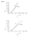
- Figures 3 and 4 shows the temperature dependency of the relation between ON-voltage V and ON-current A curve for each experimental pn diode, which is shown in Figure 1.
- Figure 3(a) shows such a curve for experimental device 1
- Figure 3(b) shows such a curve for experimental device 2.
- Figure 4 (a) shows such a curve for experimental device 3
- Figure 4 (b) shows such a curve for experimental device 4.
- These experimental devices were 1 cm 2 in chip size.
- the line T indicates the room temperature, when an ON-current for actual use is 200 A, the value of (the ON-voltage at 125°C minus the ON-voltage at room temperature) / (the ON-voltage at room temperature) is defined as the temperature coefficient. When this value is negative, the temperature coefficient is negative; and when this value is positive, the temperature coefficient is positive. In addition, the magnitude of the value represents the magnitude of the rate of change of the ON-voltage as a function of temperature.
- experimental device 1 had a temperature coefficient of +0.1 and an ON-voltage of 2.0 V at room temperature
- experimental device 2 had a temperature coefficient of +0.2 and an ON-voltage of 2.5 V
- experimental device 3 had a temperature coefficient of +0.3 and an ON-voltage of 3.0 V
- experimental device 4 had a temperature coefficient of +0.5 and an ON-voltage of 3.5 V.
- comparative device 1 had a temperature coefficient of -0.1 and an ON-voltage of 2.4 V and comparative device 2 had a temperature coefficient of +1 and an ON-voltage of 4.5 V.
- a conventional pn diode (with the anode electrode formed all over the (p) anode layer) was found to have a temperature coefficient of -0.5 and an ON-voltage of 2.3 V.
- the experimental devices (experimental devices 1 to 4) had almost the same reverse recovery current and time as the comparative devices (comparative devices 1 and 2).
- the reverse recovery time was between 630 and 650 nsec, and the reverse recovery current was between 1,100 and 1,200 A.
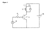
- an IGBT turn-off test circuit in Figure 5 was used to test the diodes for reverse recovery withstand voltage and which includes an IGBT 11, the experimental diode 12, a limiting resistor 13, a drive power supply 14 and a power supply 15.
- an IGBT 11 is turned ON to store energy of (1/2)LI 2 in an inductor L, and the IGBT 11 is then turned OFF. Then, a current flowing through L starts to flow through an experimental diode 12.
- a current begins to flow through the experimental diode 12 in the opposite direction to that of the current previously flowing through it, such that the original current is cancelled out.
- the experimental diode 12 enters a reverse recovery process and is turned OFF after a reverse recovery current has flowed for a period of time corresponding to the reverse recovery time. At this point, if the reverse recovery current is large and the reverse recovery time is long, reverse recovery losses increase to the point that the experimental diode 12 is destroyed.
- three experimental diodes 12 were connected in parallel.
- the experimental diodes 12 comprised conventional diodes, they were destroyed when the turn-off current of the IGBT 11 was 1,200 A.
- the diodes according to the present invention (experimental devices 1 to 4), however, were not destroyed even when the turn-off cutoff of the IGBT 11 was increased up to 6,000 A. This is because the positive temperature coefficient of the diodes according to the present invention substantially improves the balance between the currents through the three diodes connected in parallel.
- Figure 6 shows a variation of the planar pattern of the embodiment in Figure 1.
- Figure 6 (a) shows a circular-arc pattern
- Figure 6(b) shows a ring pattern
- Figure 6(c) is an island pattern.
- These planar patterns show the insulating film on the (p) anode layer.
- S 1 /S 2 area ratio
- Figure 6(c) shows square-shaped islands, they may of course be shaped like circles or polygons.
- the temperature coefficient of the pn diode can be made positive by fixing the anode electrode to a portion of the (p) anode layer and setting the ratio of area S 1 (the non-secured portion) to area S 2 (the secured portion) to between 5 and 30.
- the switching time can be reduced by means of electron beam irradiation or heavy metal diffusion. Further, the reverse recovery withstand voltage can be improved.
Landscapes
- Thyristors (AREA)
- Electrodes Of Semiconductors (AREA)
Abstract
Description
said anode electrode is secured to a part of the second conductivity-type anode layer, and the ratio of areas S1/S2 is between 5 and 30, where S1 is the area over which said anode electrode is not secured to the second conductivity-type anode layer, and S2 is the area in which the anode electrode is not secured to the second conductivity-type anode layer.
Claims (4)
- A semiconductor device comprising a first conductivity-type base layer having high resistance, a second conductivity-type anode layer formed on one surface of the first conductivity-type base layer, an anode electrode formed on a surface of the second conductivity-type anode layer, a cathode layer formed on the other surface of the first conductivity-type base layer, and a cathode electrode formed on a surface of the cathode layer, the semiconductor device being characterized in that:
said anode electrode is secured to a part of the second anode layer, and the ratio of areas S1/S2 is between 5 and 30, where S1 is the area over which said anode electrode is not fixed to the second conductivity-type anode layer, and S2 is the area in which the anode electrode is secured to the second conductivity-type anode layer. - A semiconductor device according to Claim 1, characterized in that an insulating film is interposed between said second conductivity-type anode layer and said anode electrode so that the second conductivity-type anode layer and the anode electrode are not fixed together.
- A semiconductor device according to Claim 1, characterized in that the device has a plurality of spaced areas each having said second conductivity-type anode layer and said anode electrode fixed together, and in that said areas constitute stripes, circular arcs, rings, or islands.
- A semiconductor device according to Claim 1, characterized in that said second conductivity-type anode layer, said first conductivity-type base layer, and said first conductivity-type cathode layer are subjected to electron beam irradiation or heavy metal diffusion.
Applications Claiming Priority (2)
| Application Number | Priority Date | Filing Date | Title |
|---|---|---|---|
| JP5348399 | 1999-03-02 | ||
| JP11053483A JP2000252477A (en) | 1999-03-02 | 1999-03-02 | Semiconductor device |
Publications (3)
| Publication Number | Publication Date |
|---|---|
| EP1033761A2 true EP1033761A2 (en) | 2000-09-06 |
| EP1033761A3 EP1033761A3 (en) | 2002-03-13 |
| EP1033761B1 EP1033761B1 (en) | 2006-06-14 |
Family
ID=12944102
Family Applications (1)
| Application Number | Title | Priority Date | Filing Date |
|---|---|---|---|
| EP00300603A Expired - Lifetime EP1033761B1 (en) | 1999-03-02 | 2000-01-27 | Semiconductor diode |
Country Status (4)
| Country | Link |
|---|---|
| US (1) | US6346740B1 (en) |
| EP (1) | EP1033761B1 (en) |
| JP (1) | JP2000252477A (en) |
| DE (1) | DE60028629T2 (en) |
Cited By (1)
| Publication number | Priority date | Publication date | Assignee | Title |
|---|---|---|---|---|
| DE102020119349A1 (en) | 2020-07-22 | 2022-01-27 | Infineon Technologies Austria Ag | Diode and method of making a diode |
Families Citing this family (1)
| Publication number | Priority date | Publication date | Assignee | Title |
|---|---|---|---|---|
| DE112015000206T5 (en) * | 2014-10-03 | 2016-08-25 | Fuji Electric Co., Ltd. | Semiconductor device and method of manufacturing a semiconductor device |
Family Cites Families (5)
| Publication number | Priority date | Publication date | Assignee | Title |
|---|---|---|---|---|
| JPS61269370A (en) * | 1985-05-24 | 1986-11-28 | Fujitsu Ltd | Semiconductor device |
| JP3146650B2 (en) * | 1992-07-15 | 2001-03-19 | 富士電機株式会社 | Power integrated circuit |
| DE69633004T2 (en) * | 1996-05-31 | 2004-11-25 | Stmicroelectronics S.R.L., Agrate Brianza | Vertical power bipolar transistor with integrated sensing resistor |
| JP3807023B2 (en) * | 1997-05-27 | 2006-08-09 | 富士電機デバイステクノロジー株式会社 | Power diode |
| JP3287269B2 (en) * | 1997-06-02 | 2002-06-04 | 富士電機株式会社 | Diode and manufacturing method thereof |
-
1999
- 1999-03-02 JP JP11053483A patent/JP2000252477A/en active Pending
-
2000
- 2000-01-27 EP EP00300603A patent/EP1033761B1/en not_active Expired - Lifetime
- 2000-01-27 DE DE60028629T patent/DE60028629T2/en not_active Expired - Fee Related
- 2000-03-02 US US09/517,153 patent/US6346740B1/en not_active Expired - Lifetime
Cited By (4)
| Publication number | Priority date | Publication date | Assignee | Title |
|---|---|---|---|---|
| DE102020119349A1 (en) | 2020-07-22 | 2022-01-27 | Infineon Technologies Austria Ag | Diode and method of making a diode |
| US11664464B2 (en) | 2020-07-22 | 2023-05-30 | Infineon Technologies Austria Ag | Diode and method of producing a diode |
| US12132122B2 (en) | 2020-07-22 | 2024-10-29 | Infineon Technologies Austria Ag | Single chip power diode and method of producing a single chip power diode |
| DE102020119349B4 (en) * | 2020-07-22 | 2025-06-18 | Infineon Technologies Austria Ag | Single-chip power diode and method for manufacturing a single-chip power diode |
Also Published As
| Publication number | Publication date |
|---|---|
| EP1033761B1 (en) | 2006-06-14 |
| US6346740B1 (en) | 2002-02-12 |
| EP1033761A3 (en) | 2002-03-13 |
| JP2000252477A (en) | 2000-09-14 |
| DE60028629T2 (en) | 2006-10-12 |
| DE60028629D1 (en) | 2006-07-27 |
Similar Documents
| Publication | Publication Date | Title |
|---|---|---|
| CN100423287C (en) | Reverse conduction type semiconductor element and manufacturing method thereof | |
| US6278140B1 (en) | Insulated gate thyristor | |
| US7169634B2 (en) | Design and fabrication of rugged FRED | |
| CN104969360B (en) | Semiconductor device | |
| US8829519B2 (en) | Semiconductor device | |
| Schlangenotto et al. | Improved recovery of fast power diodes with self-adjusting p emitter efficiency | |
| CN102903633B (en) | Method for making field stop insulated gate bipolar transistor with anode shorted | |
| US20030030120A1 (en) | Diode and method for manufacturing the same | |
| US7557386B2 (en) | Reverse conducting IGBT with vertical carrier lifetime adjustment | |
| JPH04229660A (en) | Power transistor device provided with very deep concentration-added region | |
| US6603153B2 (en) | Fast recovery diode and method for its manufacture | |
| US6507050B1 (en) | Thyristors having a novel arrangement of concentric perimeter zones | |
| US5414290A (en) | IGBT with self-aligning cathode pattern and method for producing it | |
| JPH01258476A (en) | High breakdown voltage semiconductor device and manufacture thereof | |
| JP3737524B2 (en) | Rectification semiconductor device | |
| US4901120A (en) | Structure for fast-recovery bipolar devices | |
| US7868352B2 (en) | Silicon break over diode | |
| EP0767500A2 (en) | Power semiconductor device with lattice defects | |
| EP1033761B1 (en) | Semiconductor diode | |
| US3906545A (en) | Thyristor structure | |
| Stoisiek et al. | A 200-A/2000-V MOS-GTO with improved cell design | |
| EP0878849A2 (en) | Power diode | |
| US6683328B2 (en) | Power semiconductor and fabrication method | |
| JPH05136015A (en) | Semiconductor device | |
| JP2001177114A (en) | Semiconductor device |
Legal Events
| Date | Code | Title | Description |
|---|---|---|---|
| PUAI | Public reference made under article 153(3) epc to a published international application that has entered the european phase |
Free format text: ORIGINAL CODE: 0009012 |
|
| AK | Designated contracting states |
Kind code of ref document: A2 Designated state(s): AT BE CH CY DE DK ES FI FR GB GR IE IT LI LU MC NL PT SE Kind code of ref document: A2 Designated state(s): DE FR GB |
|
| AX | Request for extension of the european patent |
Free format text: AL;LT;LV;MK;RO;SI |
|
| PUAL | Search report despatched |
Free format text: ORIGINAL CODE: 0009013 |
|
| AK | Designated contracting states |
Kind code of ref document: A3 Designated state(s): AT BE CH CY DE DK ES FI FR GB GR IE IT LI LU MC NL PT SE |
|
| AX | Request for extension of the european patent |
Free format text: AL;LT;LV;MK;RO;SI |
|
| 17P | Request for examination filed |
Effective date: 20020307 |
|
| AKX | Designation fees paid |
Free format text: DE FR GB |
|
| GRAP | Despatch of communication of intention to grant a patent |
Free format text: ORIGINAL CODE: EPIDOSNIGR1 |
|
| GRAS | Grant fee paid |
Free format text: ORIGINAL CODE: EPIDOSNIGR3 |
|
| GRAA | (expected) grant |
Free format text: ORIGINAL CODE: 0009210 |
|
| AK | Designated contracting states |
Kind code of ref document: B1 Designated state(s): DE FR GB |
|
| REG | Reference to a national code |
Ref country code: GB Ref legal event code: FG4D |
|
| REF | Corresponds to: |
Ref document number: 60028629 Country of ref document: DE Date of ref document: 20060727 Kind code of ref document: P |
|
| ET | Fr: translation filed | ||
| PLBE | No opposition filed within time limit |
Free format text: ORIGINAL CODE: 0009261 |
|
| STAA | Information on the status of an ep patent application or granted ep patent |
Free format text: STATUS: NO OPPOSITION FILED WITHIN TIME LIMIT |
|
| 26N | No opposition filed |
Effective date: 20070315 |
|
| REG | Reference to a national code |
Ref country code: GB Ref legal event code: 746 Effective date: 20090216 |
|
| PGFP | Annual fee paid to national office [announced via postgrant information from national office to epo] |
Ref country code: DE Payment date: 20090123 Year of fee payment: 10 |
|
| PGFP | Annual fee paid to national office [announced via postgrant information from national office to epo] |
Ref country code: GB Payment date: 20090121 Year of fee payment: 10 |
|
| PGFP | Annual fee paid to national office [announced via postgrant information from national office to epo] |
Ref country code: FR Payment date: 20090113 Year of fee payment: 10 |
|
| GBPC | Gb: european patent ceased through non-payment of renewal fee |
Effective date: 20100127 |
|
| REG | Reference to a national code |
Ref country code: FR Ref legal event code: ST Effective date: 20100930 |
|
| PG25 | Lapsed in a contracting state [announced via postgrant information from national office to epo] |
Ref country code: FR Free format text: LAPSE BECAUSE OF NON-PAYMENT OF DUE FEES Effective date: 20100201 |
|
| PG25 | Lapsed in a contracting state [announced via postgrant information from national office to epo] |
Ref country code: DE Free format text: LAPSE BECAUSE OF NON-PAYMENT OF DUE FEES Effective date: 20100803 |
|
| PG25 | Lapsed in a contracting state [announced via postgrant information from national office to epo] |
Ref country code: GB Free format text: LAPSE BECAUSE OF NON-PAYMENT OF DUE FEES Effective date: 20100127 |