EP1033758A2 - Bipolar transistor and process for fabricating the same - Google Patents
Bipolar transistor and process for fabricating the same Download PDFInfo
- Publication number
- EP1033758A2 EP1033758A2 EP00104172A EP00104172A EP1033758A2 EP 1033758 A2 EP1033758 A2 EP 1033758A2 EP 00104172 A EP00104172 A EP 00104172A EP 00104172 A EP00104172 A EP 00104172A EP 1033758 A2 EP1033758 A2 EP 1033758A2
- Authority
- EP
- European Patent Office
- Prior art keywords
- conduction type
- region
- base region
- emitter
- area
- Prior art date
- Legal status (The legal status is an assumption and is not a legal conclusion. Google has not performed a legal analysis and makes no representation as to the accuracy of the status listed.)
- Withdrawn
Links
Images








Classifications
-
- H—ELECTRICITY
- H10—SEMICONDUCTOR DEVICES; ELECTRIC SOLID-STATE DEVICES NOT OTHERWISE PROVIDED FOR
- H10D—INORGANIC ELECTRIC SEMICONDUCTOR DEVICES
- H10D64/00—Electrodes of devices having potential barriers
- H10D64/20—Electrodes characterised by their shapes, relative sizes or dispositions
- H10D64/23—Electrodes carrying the current to be rectified, amplified, oscillated or switched, e.g. sources, drains, anodes or cathodes
- H10D64/231—Emitter or collector electrodes for bipolar transistors
-
- H—ELECTRICITY
- H10—SEMICONDUCTOR DEVICES; ELECTRIC SOLID-STATE DEVICES NOT OTHERWISE PROVIDED FOR
- H10D—INORGANIC ELECTRIC SEMICONDUCTOR DEVICES
- H10D10/00—Bipolar junction transistors [BJT]
- H10D10/01—Manufacture or treatment
- H10D10/051—Manufacture or treatment of vertical BJTs
-
- H—ELECTRICITY
- H10—SEMICONDUCTOR DEVICES; ELECTRIC SOLID-STATE DEVICES NOT OTHERWISE PROVIDED FOR
- H10D—INORGANIC ELECTRIC SEMICONDUCTOR DEVICES
- H10D10/00—Bipolar junction transistors [BJT]
- H10D10/40—Vertical BJTs
- H10D10/421—Vertical BJTs having both emitter-base and base-collector junctions ending at the same surface of the body
-
- H—ELECTRICITY
- H10—SEMICONDUCTOR DEVICES; ELECTRIC SOLID-STATE DEVICES NOT OTHERWISE PROVIDED FOR
- H10D—INORGANIC ELECTRIC SEMICONDUCTOR DEVICES
- H10D64/00—Electrodes of devices having potential barriers
- H10D64/20—Electrodes characterised by their shapes, relative sizes or dispositions
- H10D64/27—Electrodes not carrying the current to be rectified, amplified, oscillated or switched, e.g. gates
- H10D64/281—Base electrodes for bipolar transistors
Definitions
- the present invention relates to a semiconductor device which is useful for the application to a BiCMOS transistor wherein a bipolar transistor and a CMOS transistor are intermixed, and a process for fabricating the same; and in particular to a semiconductor device wherein a bipolar transistor is improved, and a process for fabricating the same.
- analogue/digital intermixing LSI large scale integrated circuit
- PHS personal handy system
- a portable telephone a communication terminal for a network, and the like.
- CMOS transistor which can easily make its consumption electric power small, is used as a digital circuit corresponding to high-speed action in the analog/digital intermixing LSI.
- an analogue circuit corresponding to high-speed action a high-performance bipolar transistor is used, and the action of the circuit is performed at a high frequency of several hundreds of MHz to several tens of GHz. Therefore, in order to use the analogue circuit at higher frequencies, it is necessary to improve high frequency characteristics of the bipolar transistor.
- fT cut-off frequency
- fmax maximum oscillation frequency
- fmax is an index of driving ability of the bipolar transistor
- This fmax is approximately represented by the following formula: fmax ⁇ (fT/(8 ⁇ ⁇ Rb ⁇ Ccb)) wherein Rb represents a base resistance, and Ccb represents a capacity between collector and base (base-to-collector capacitance).
- the expression representing the tax includes fT, as is clearly from the formula 1. Therefore, the fmax shows the total performance of the high frequency characteristics of the bipolar transistor. It can be said that as this value is larger, the high frequency characteristics are better.
- FIG. 1 is a plan view showing an arrangement of respective layers of a conventional bipolar transistor.
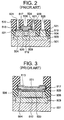
- FIG. 2 is a sectional view taken along F-F line of FIG. 1.
- FIG. 3 is a sectional view taken along G-G line of FIG. 1.
- a high-concentration N type buried layer 503 is formed on a P type semiconductor substrate 501.
- an N type epitaxial area 504 is formed to cover the buried layer 503.
- a pedestal collector 512 which is an N type area having an impurity concentration that is in the middle of concentrations of the epitaxial area 504 and the buried layer 503, is formed just under a high-concentration N type diffusion layer 520, which is an emitter region.
- the collector area of the bipolar transistor is composed of the high-concentration N type buried layer 503, the N type epitaxial area 504 and pedestal collector 512.
- An element separation oxide film 506 is formed in the surface of the N type epitaxial area 504. This element isolation oxide film 506 is formed to surround an intrinsic base region 509, a high-concentration P type diffusion layer 518, and a high-concentration N type diffusion layer 519. The intrinsic base region 509 and the high-concentration P type diffusion layer 518 are electrically isolated from the high-concentration N type diffusion area 519 by means of the element isolation oxide film 506.
- a high-concentration N type diffusion layer 520 is formed inside the intrinsic base region 509. This high-concentration N type diffusion layer 520 makes an emitter region. An emitter leading-out electrode 513 made of polysilicon is formed to connect this emitter region.
- a titanium silicide film 521 is formed on the surface of this emitter electrode 513.
- the titanium silicide film 521 is also formed on the surface of the high-concentration P type diffusion layer 518 to make an extrinsic base region (a graft base region).
- An interlayer dielectric 522 is formed on its whole surface. In this interlayer dielectric 522, base contact holes 524 are made in its extrinsic base region, and a contact hole 525 for collector plug is made in the collector plug region.
- An emitter contact hole 526 is made in the interlayer dielectric 522 just above the emitter electrode.
- the high-concentration P type diffusion layer 518 the surface of which is covered with the titanium silicide film 521, is divided into right and left portions in FIG. 21 by means of the emitter leading-out electrode 513 composed of the second conductive film, the surface of which is covered with the titanium silicide film 521.
- the base contact holes 524 are made at right and left positions adjacent to the emitter leading-out electrode 513 composed of the second conductive film, so as to make a form of the arrangement for leading out a non-illustrated metal wiring for leading-out of the base electrode.
- the plan view layout according to this method is as follows: the surface of the high-concentration P type diffusion layer 518 is covered with the titanium silicide film having a sheet resistance of about 5 ⁇ /square and the non-illustrated metal wiring for leading-out of the base electrode is led out at both ends of the emitter leading-out electrode 513 composed of the second conductive film. Therefore, this layout makes it possible to make the base resistance lower than the layout wherein the surface of the high-concentration P type diffusion layer 518 is not covered with any titanium silicide.
- the above-mentioned known publication states that for this reason the maximum oscillation frequency fmax can be raised up to 54 GHz when the voltage between the collector and the emitter (C-E voltage) is 2.5 V.
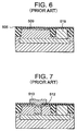
- the high-concentration N type buried layer 503 is formed on the P type semiconductor substrate 501.
- the N type epitaxial area 504 of 1 ⁇ m in thickness is formed on the P type semiconductor substrate 501 to cover the high-concentration N type buried layer 503.
- the element isolation oxide film 506 is formed on the epitaxial area 504 by the LOCOS (Local oxidation of Silicon) method. Furthermore, the first oxide film 505 is formed on the epitaxial area 504 to have a thickness of 12 nm.
- LOCOS Local oxidation of Silicon
- the high-concentration N type diffusion layer 519 is formed, in the portion which becomes the collector plug region between the element isolation oxide films 506, inside the epitaxial area 504 by ion implantation of, for example, phosphorus. Furthermore, boron is ion-implanted into the epitaxial area 504 at an energy of 7 keV to form the intrinsic base region 509 in the epitaxial area 504.
- a widow for forming an emitter region is made in the first oxide film 505.
- Phosphorus is then implanted into the epitaxial area 504 at an energy of 550 keV to form the pedestal collector 512 therein.
- the second conductive layer comprising polysilicon containing arsenic is grown on the whole surface to have a thickness of 250 nm. This is then patterned to form the emitter leading-out electrode 513 comprising the second conductive film on the opened window in the first oxide film 505.
- a side wall 517 comprising an oxide film and having a thickness of 150 nm is formed on the side wall of the emitter leading-out electrode 513.
- Boron is ion-implanted therein at an energy of 10 keV to form the high-concentration P type diffusion layer 518, with self alignment, in the surface of the epitaxial area 504, using the emitter leading-out electrode 513 and the side wall 517 as masks.
- the resultant is subjected to RTA (Rapid Thermal Annealing) treatment, for example, at 1025°C for 20 seconds to diffuse arsenic from the emitter leading-out electrode 513, which is the second conductive film containing arsenic, into the intrinsic base region 509.
- the high-concentration N type diffusion layer 520 is formed in the intrinsic base region 509.
- a known silicide technique is used to form the titanium silicide film 521, with self alignment, on the surface of the emitter leading-out electrode 513, the high-concentration P type diffusion layer 518 and the high-concentration N type diffusion layer 519.
- the interlayer dielectric 522 is formed on the whole surface.
- the contact holes 526, 524 and 525 are made, at the positions corresponding to the emitter leading-out electrode 513, the high-concentration P type diffusion layer 518 and the high-concentration N type diffusion layer 519, in the interlayer dielectric 522.
- a contact plug 527 comprising a barrier metal composed of W and, for example, Ti/TiN is buried in the contact holes to form a pattern of a metal wiring 528 on the interlayer dielectric 522.
- the extrinsic base region composed of the high-concentration P type diffusion layer 518 and the titanium silicide film 521 is formed at both sides of the emitter electrode 513, and the base contact hole 524 for leading out base electrical potential is made in each of the extrinsic base regions. Therefore, the extrinsic base region, and the metal wirings 528 for leading out base electrical potential are present at both sides of the emitter electrode 513 so that the collector-base capacity Ccb cannot be made small.
- the extrinsic base region (high-concentration P type diffusion layer 518) and the base contact hole 524 are disposed at only one side of the emitter electrode 513 to make the collector-base capacity Ccb small, the base resistance Rb increases. It is evident from the formula (1) that when the capacity Ccb or Rb increases in this way, the maximum oscillation frequency fmax drops to deteriorate the characteristics as a bipolar transistor. Accordingly, the conventional bipolar transistors have a problem that a sufficiently large maximum oscillation frequency cannot be obtained.
- an object of the present invention is to provide a semiconductor device making it possible to reduce the base resistance Rb and the collector-base capacity Ccb to make the maximum oscillation frequency fmax sufficiently large and improve transistor characteristics, and a process for fabricating the same.
- a first semiconductor device of the present invention comprises a first conduction type semiconductor substrate, a second conduction type area formed on a surface of the semiconductor substrate, a first conduction type intrinsic base region formed on a surface of the second conduction type area, an extrinsic base region surrounding the intrinsic base region, a second conduction type emitter region formed in the intrinsic base region, an emitter electrode contacting the emitter region, a second conduction type collector plug region formed in the second conduction type area, an element isolation area for isolating the first conduction type intrinsic base region and the extrinsic base region electrically from the second conduction type collector plug region, and a cobalt silicide film formed to surround the emitter electrode, as viewed from above, on the extrinsic base region.
- a second semiconductor device of the present invention comprises a first conduction type semiconductor substrate, a second conduction type buried layer formed in the semiconductor substrate, a second conduction type epitaxial layer formed on the buried layer, a first conduction intrinsic base region formed on a surface of the epitaxial layer, an extrinsic base region surrounding the intrinsic base region, a second conduction type emitter region formed in the intrinsic base region, an emitter electrode contacting the emitter region, a second conduction type collector plug region formed on the buried layer, an element isolation area for isolating the intrinsic base region and the extrinsic base region electrically from the collector plug region, and a cobalt silicide formed to surround the emitter electrode, as viewed from above, on the extrinsic base region.
- a third semiconductor device of the present invention comprises a first conduction type semiconductor substrate, second conduction type first and second well areas formed on a surface of the semiconductor substrate, a first conduction type third well area formed on the surface of the semiconductor substrate between the first and second well areas, a second conduction type MOS transistor formed in the first well area, a first conduction type MOS transistor formed on the third well area and a bipolar transistor formed in the second well area.
- Said bipolar transistor comprises a first conduction type intrinsic base region formed on the surface of the second well area, an extrinsic base region surrounding the intrinsic base region, a second conduction type emitter region formed in the intrinsic base region, an emitter electrode contacting the emitter region, a second conduction type collector plug region formed in the second conduction type area, an element isolation area for isolating the first conduction type intrinsic base region and the extrinsic base region electrically from the second conduction type collector plug region, and a cobalt silicide film formed to surround the emitter electrode, as viewed from above, on the extrinsic base region.
- one base contact connected with the extrinsic base region is preferably arranged for the single emitter electrode.
- a fourth semiconductor device of the present invention comprises a first conduction type semiconductor substrate, a second conduction type area formed on a surface of the semiconductor substrate, a pair of first conduction type intrinsic base regions formed on a surface of the second conduction type area, a first conduction type extrinsic base region formed to surround the intrinsic base regions as viewed from above, a second conduction type emitter region formed in the respective intrinsic base regions, a pair of emitter electrodes contacting the emitter region, a collector plug region formed in the second conduction type area, an element isolation area for isolating the extrinsic base region electrically from the collector plug region, and a cobalt silicide film formed to surround the respective emitter electrodes, as viewed from above, on the extrinsic base region.
- This semiconductor device may comprise a pair of base contacts arranged in the extrinsic base region at both outsides of the emitter electrode and connected with the extrinsic base region, or a base contact area arranged in the extrinsic base region between the pair of the emitter electrodes and connected with the extrinsic base region.
- a process for fabricating a semiconductor device of the present invention comprises the steps of forming an element isolation area for dividing a base formation planning area from a collector formation planning area, and a second conduction type area including these planning areas on a first conduction type silicon substrate; forming a first conduction type intrinsic base region on a surface of the second conduction type area of the base formation planning area; forming an insulating film on the whole surface thereof and making an opening in the emitter formation planning area of the insulating film; forming an emitter electrode comprising polysilicon film containing a second conduction type impurity on the insulating film to fill up in the opening of the insulating film; forming an emitter region contacting said emitter electrode in the intrinsic base region, forming an extrinsic base region surrounding the intrinsic base region in the intrinsic base region not converted with the emitter electrode, and forming a collector plug region in the collector formation planning area; forming a cobalt film on the whole surface and then reacting the cobalt film with the silicon of the substrate to form
- the cobalt silicide film is formed on the extrinsic base region to surround the periphery of the emitter electrode, and the contact contacting this cobalt silicide film is arranged at only one side of the emitter electrode.
- Any conventional titanium silicide film has a narrow line effect. Thus, if its width is made small, its layer resistance increase. Conventionally, wirings for leading out base voltage are arranged at both sides of the emitter electrode to lower the base resistance as much as possible. Therefore, in conventional bipolar transistors, the width of the titanium silicide film 521 on the high-concentration P type diffusion layer 518 cannot be made narrow. This is a reason why the distance between the emitter electrode 513 and the field insulating film 506 cannot be made small and the collector-base capacity Ccb cannot be reduced.
- the cobalt silicide film is used instead of the titanium silicide and further the cobalt silicide film is formed in a ring form so as to surround the emitter electrode.
- the resistance when an electric current is passed from the intrinsic base region to the cobalt silicide film through the extrinsic base region that is, the resistance when an electric current is passed in a vertical direction, is larger than the corresponding resistance in the case of using the titanium silicide. Therefore, even if the contact is disposed at only one side of the emitter electrode as in the present embodiment, the base resistance Rb can be made sufficiently small.
- the contact and the wiring connecting with it are formed at only one side of the emitter electrode, the distance between the emitter electrode and the filed insulating film, that is, the width of the base region, can be made small so that the collector-base capacity Ccb can be made small. According to the present invention, therefore, the maximum oscillation frequency fmax can be improved to improve transistor characteristics.
- FIG. 11 is a plan view showing an arrangement of respective layers of a bipolar transistor according to a first embodiment of the present invention.
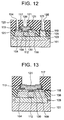
- FIG. 12 is a sectional view taken along A-A line of FIG. 11.
- FIG. 13 is a sectional view taken along B-B line of FIG. 11.
- a high-concentration N type buried layer 103 is formed on a P type semiconductor substrate 101.
- An N type epitaxial area 104 is formed on the substrate 101 to cover the high-concentration N type buried layer.
- a pedestal collector 112 which is an N type area having an impurity concentration that is in the middle of concentrations of the N type epitaxial area 104 and the high-concentration N type buried layer 103, is formed just under a high-concentration N type diffusion layer 120, which is an emitter region in the N type epitaxial area 104.
- the high-concentration N type buried layer 103, the N type epitaxial area 104 and the pedestal collector 112 makes the collector area of the bipolar transistor.
- a high-concentration P type diffusion layer 118 is formed in the surface of the substrate to surround an intrinsic base region 109. This high-concentration P type diffusion layer makes an extrinsic base region.
- an element isolation oxide film 106 is formed on the surface of the N type epitaxial area 104.
- This element isolation oxide film 106 is formed to surround the intrinsic base region 190, the high-concentration P type diffusion layer 118 (extrinsic base region), and the high-concentration N type diffusion layer 119 (collector plug region).
- the intrinsic base region 109 and the high-concentration P type diffusion layer 118 are electrically isolated from the collector plug region composed of the high-concentration N type diffusion area 119 by means of the element isolation oxide film 106.
- This high-concentration P type diffusion layer 118 and the cobalt silicide film 121 make an extrinsic base region. Besides, the surface of the collector plug region comprising the high-concentration N type diffusion layer 119 is covered with the cobalt silicide film 121.
- An interlayer dielectric 123 is formed on its whole surface.
- a base contact hole 124 is made above the high-concentration P type diffusion layer 118 of an opposite side to the collector plug electrode in relative to the emitter leading-out electrode 113, so as to make it possible to lead out a non-illustrated metal wiring for leading out the base electrode.
- a contact hole 125 for collector plug is made in the interlayer dielectric 123 above the collector plug region comprising the high-concentration N type diffusion layer 119.
- a contact hole 126 for emitter leading-out is made above the emitter leading-out electrode 113 whose surface is covered with the cobalt silicide film 121.
- the bipolar transistor of the present embodiment having the above-mentioned structure.
- the high-concentration P type diffusion layer 118 extendrinsic base region
- cobalt silicide film 121 is formed in a ring form to surround the periphery of the emitter leading-out electrode 113 comprising the second conductive film.
- the contact hole 124 for leading-out the base electrode and the non-illustrated metal wiring can be arranged at only one side of the emitter leading-out electrode 113 in the present embodiment so that the base contact can be led out from only one side of the emitter electrode. In this way, the size of the bipolar transistor can be made small according to the present invention.
- the cobalt silicide film is used instead of any conventional titanium silicide film.
- the resistance when an electric current is passed from the intrinsic base region 109 to the cobalt silicide film 121 through the extrinsic base region 118, that is, the resistance when an electric current is passed in a vertical direction, is larger than the corresponding resistance in the case of using the titanium silicide. Therefore, even if the base contact (contact hole 124) is disposed at only one side of the emitter electrode 113 as in the present embodiment, the base resistance Rb can be made sufficiently small.
- the contact and the wiring for connecting it are formed at only one side of the emitter electrode, the distance between the emitter electrode and the filed insulating film, that is, the width of the base region, can be made small so that the collector-base capacity Ccb can be made small. According to the present invention, therefore, the maximum oscillation frequency fmax can be improved to improve transistor characteristics.
- the above-mentioned embodiment is an embodiment wherein the present invention is applied to a bipolar transistor, but the effect of the present invention is made still more remarkable by applying the present invention to a BiCMOS wherein a bipolar transistor and a CMOS transistor are made in the same single chip.
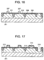
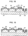
- FIGS. 14-20 are sectional views showing a second embodiment of the present invention wherein the present invention is applied to a BiCMOS.
- FIGs. 14-20 are sectional views showing a process for fabricating the BiCMOS in the order of its steps. Referring to FIG. 20, the sectional structure of the BiCMOS of the present second embodiment will be first described.
- a P type well area 204 and a first N type well area 203 for constituting a CMOS, and a second N type well area 208 for constituting a bipolar transistor are formed on a P type semiconductor substrate 201.
- a gate electrode 207 whose upper surface is covered with a cobalt silicide film 221, and a side wall 217 on the side thereof are formed.
- a high-concentration N type diffusion layer 219 is formed beneath the side wall 217 to self-align with the N type diffusion layer 210 and the side wall 217.
- a cobalt silicide film 221 is formed on the surface of the area 219.
- the N type diffusion layer 210 and the high-concentration N type diffusion layer 219 constitute the LDD source/drain area of an NMOS.
- a gate electrode 207 Inside the first N type well area 203, a gate electrode 207 whose upper surface is covered with a cobalt silicide film 221, and a side wall 217 on the side thereof is formed.
- a high-concentration P type diffusion layer 218 is famed beneath the side wall 217 to self-align with the P type diffusion layer 211 and the side wall 217.
- a cobalt silicide film 221 is formed on the surface of the area 218.
- the P type diffusion layer 211 and the high-concentration P type diffusion layer 218 constitute the LDD source/drain area of a PMOS.
- an element isolation oxide film 202 is present to isolate a collector plug portion from an emitter/base forming area.
- a trench collector 215 is formed in the collector plug portion.
- a side wall composed of a second LDD oxide film 216 is formed on the side wall of the trench collector 215.
- a high-concentration N type diffusion layer 219 is formed at the bottom of the trench collector 215 to self-align with the side wall composed of the second LDD oxide film 216.
- a cobalt silicide film 221 is formed on the surface of the area 219.
- an emitter leading-out electrode composed of the second conductive film 213 is connected with the high-concentration N type diffusion layer 220 through a contact opened in the first LDD oxide film 212.
- the first oxide film 214 is formed on the emitter leading-out electrode composed of the second conductive film 213.
- a side wall composed of the second LDD oxide film 216 is formed on the side wall of the emitter leading-out electrode composed of the second conductive film 213.
- the high-concentration P type diffusion layer 218 is toned to self-align with the side wall composed of the second LDD oxide film 216.
- the cobalt silicide film 221 is formed on the surface of the area 218.
- the element isolation oxide film 202, the P type well area 204, and the first N type well area 203 are first toned on the P type semiconductor substrate 201.
- the gate oxide film 205 having a thickness of, for example, 2-4 nm and the first conductive film 206 having a thickness of, for example, 10-25 nm and comprising amorphous silicon, polycrystal silicon, amorphous silicon containing phosphorus, arsenic or boron, or the like.
- the first conductive film 206 is patterned to form the gate electrode 207.
- the N type diffusion layer 210 and the P type diffusion layer 211 are formed to self-align with the gate electrode.
- Phosphorus is implanted at an energy of 400-1000 keV to form the second N type well area 208.
- boron or BF 2 is implanted at an energy of at most 4 keV or 15 keV, respectively, to form the intrinsic base region 209.
- the first LDD oxide film 212 of, for example, 20-80 nm in thickness is grown, and then a window for the emitter is made.
- the second conductive film 213 having a thickness of, for example, 150-300 nm and comprising amorphous silicon, polycrystal silicon, amorphous silicon containing phosphorus or arsenic, or the like, and the first oxide film 214 having a thickness of, for example, 100-200 nm are grown.
- Photolithographic technique is used to form the emitter leading-out electrode. By over-etching at the time of patterning this emitter leading-out electrode, a trench collector 215 of, for example, 400-700 nm in depth is formed.
- the second LDD oxide film 216 having a thickness of, for example, 40-100 nm is grown.
- This LDD oxide film 216 is subjected to anisotropic etching to form the side wall 217 composed of the first LDD oxide film 212 and the second LDD oxide film 216 on the side of the gate electrode 207 and form the side wall composed of the second LDD oxide film 216 on the sides of the second conductive film 213 and the trench collector 215.
- Ion implantation is performed to self-align with these side walls. In this way, the high-concentration P type diffusion layers area 218 and the high-concentration N type diffusion layer 219 are formed.
- the impurity contained in the second conductive film 213 is diffused by RTA so that the high-concentration N type diffusion layer 220 is formed.
- cobalt is sputtered to form the cobalt film on the whole surface.
- the silicon layer on the surface of the semiconductor substrate is reacted with cobalt to form the cobalt silicide film 221.
- any unreacted cobalt film is removed by etching.
- the interlayer dielectric 222 is formed to open the contact at a given position.
- the contact plug 223 comprising a barrier metal composed of W and, for example, Ti/TiN is then buried in the contact.
- a metal wiring 224 for connecting the contact plug 223 is formed on the interlayer dielectric 222.
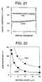
- FIG. 21 is a graph showing contact resistance of a silicide film formed on the surface of the high-concentration P type diffusion layer, in which its horizontal axis represents applied voltage and its vertical axis represents contact resistance at the time of sending an electrical current in a so-called vertical direction.
- This graph shows dependency of the contact resistance upon the applied voltage in the case of forming a titanium silicide film and a cobalt silicide film as silicide films.
- the electric current sent in the vertical direction means an electric current that has run from the high-concentration P type diffusion layer to the silicide film in the thickness direction thereof and then run the contact plug contacting the silicide film.
- the contact resistance is a contact resistance between the silicide film and the high-concentration P type diffusion layer.
- FIG. 22 is a graph showing the dependency of base resistance upon emitter length in the case of forming the titanium silicide film or the cobalt silicide, in which its horizontal axis represents the emitter length and the vertical axis represents the base resistance. As shown in FIGs. 21-23, this graph shows the dependency of base resistance upon emitter length in the bipolar transistor having a plan view layout wherein the base contact 125 is arranged at one side of the emitter electrode 113 composed of the second conductive film.
- the contact resistance on the high-concentration P type diffusion layer is made smaller by about one figure. In this case, therefore, the base resistance can be made smaller than in the case of using the titanium silicide film.
- the base resistance can be reduced to about halt of the base resistance in the case of the titanium silicide in the prior art.
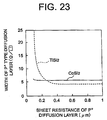
- FIG. 23 is a graph showing the affect on the relationship between the width of a P + type diffusion layer and the sheet resistance thereof by a cobalt silicide film and a titanium silicide film, wherein its horizontal axis represents the width and its vertical axis represents the sheet resistance. That is, this graph shows the dependency of sheet resistance upon the width of the diffusion layer in the case of forming a titanium silicide film and a cobalt silicide film on the surface of the high-concentration P type diffusion layer.
- the sheet resistance in the case of using the cobalt silicide film of the present invention is slightly higher than that in the case of using the titanium silicide film in the prior art: the sheet resistance of the former is about 6 ⁇ /square and that of the latter is about 5 ⁇ /square. In the case of the titanium silicide film, however, its sheet resistance does not rise even within the range in which the width of the diffusion layer is smaller than 0.3 ⁇ m.
- the sheet resistance of the titanium silicide film rises sharply in the range in which the width of the diffusion layer is smaller than 0.3 ⁇ m while the sheet resistance of the cobalt silicide film hardly rises and keeps low values in the same range. Therefore, in the present invention using the cobalt silicide film, which is different from the case using the titanium silicide film, the width of the diffusion layer can be made smaller without any rise in the sheet resistance. Moreover, the collector-base capacity Ccb can be reduced by using a plan view layout wherein the base contact 125 is made at one side of the polysilicon emitter electrode 113 shown in FIGs. 11-13.
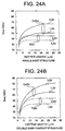
- FIG. 24A shows the dependency of fmax of a bipolar transistor upon emitter length, the transistor having a plan view layout wherein the base contact 125 is made at one side of the polysilicon emitter electrode 113 shown in FIGs. 11-13 in the case wherein the titanium silicide film or the cobalt silicide film is formed on the surface of the high-concentration P type diffusion layer (this layout is referred to as a single base structure, hereinafter).
- FIG. 24B shows the dependency of fmax of a conventional bipolar transistor upon emitter length, the transistor having a plan view layout wherein the base contacts 525 are made at both sides of the emitter electrode 513 comprising the second conductive film and shown in FIGs. 1-3 in the case wherein the titanium silicide film or the cobalt silicide film is formed on the surface of the high-concentration P type diffusion layer (this layout is referred to as a double base structure, hereinafter).
- the collector-base capacity Ccb and the base resistance Rb can be simultaneously reduced.
- the inventor performed experiments, using the layout shown in the plan views related to the present invention.
- fmax was 46 GHz (the collector-emitter voltage: 3.3 V) at the time of using the titanium silicide film.
- fmax was 67 GHz (the collector-emitter voltage: 3.3 V) at the time of using the cobalt silicide film. Namely, fmax was able to be raised by about 1.45 times, as shown in FIG. 24A.
- fmax was 54 GHz (the collector-emitter voltage: 3.3 V).
- fmax was 80 GHz (the collector-emitter voltage: 3.3 V). Namely, fmax was able to be raised by about 1.48 times.
- basic blocks of a bipolar transistor generally used in an analogue circuit have a plurality of metal leading-out wirings for its emitter, base and collector in order to improve factors having an influence on its analogue characteristics, for example, its base resistance and high frequency noise (Nf).
- Nf high frequency noise
- FIG. 9 and FIG. 10 is a sectional view taken along E-E line thereof.
- a plan view layout in the prior art has contacts for the following from the left side: a collector/a base/an emitter/a base/an emitter/a base/a collector.
- reference numbers 534 and 533 represent wirings for the collector, the base and the emitter, and contact plugs connecting to the wiring 534.
- the contact plugs are buried in a non-illustrated interlayer dielectric.
- a bipolar transistor shown in FIG. 25 of the third embodiment in the present invention
- its base resistance Rb can be reduced by using a cobalt silicide film. Therefore, it is sufficient that a pair of base contacts are disposed for a pair of emitter electrodes 113.
- its plan view layout can be made into a layout having six contacts for a collector/a base/an emitter/an emitter/a base/a collector.
- one metal wiring for extrinsic base can be cut down, as compared with the prior art. Therefore, the collector-base capacity Ccb can be reduced. This makes it possible to improve the maximum oscillation frequency fmax still more.
- reference numbers 134 and 113 represent wirings for the collector, the base and the emitter, and contact plugs connecting with the wiring 134, respectively. The contact plugs are buried in a non-illustrated interlayer dielectric.
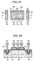
- FIG. 27 is a plan view showing a layout of respective layers of a bipolar transistor according to a fourth embodiment.
- FIG. 28 is a sectional view taken along D-D line of FIG. 27.
- the embodiment shown in FIGs. 27 and 28 has a plan view layout comprising five contacts for a collector/an emitter/a base/an emitter/a collector. Therefore, one metal wiring for extrinsic base can be cut, as compared with the third embodiment shown in FIGs. 25 and 26, so that the collector-base capacity Ccb can be reduced still more. For this reason, the product of the base resistance Rb and the collector-base capacity Ccb can be reduced so that the maximum oscillation frequency fmax can be improved still more.
- a cobalt silicide film for extrinsic base is formed to surround an emitter electrode, as viewed from above. Therefore, both the base resistance Rb and the collector-base capacity Ccb can be reduced to improve the maximum oscillation frequency fmax. This makes it possible to improve the transistor characteristics remarkably.
Landscapes
- Bipolar Transistors (AREA)
- Bipolar Integrated Circuits (AREA)
- Electrodes Of Semiconductors (AREA)
- Metal-Oxide And Bipolar Metal-Oxide Semiconductor Integrated Circuits (AREA)
Abstract
Description
Claims (18)
- A semiconductor device, comprising:a first conduction type semiconductor substrate;a second conduction type area formed on a surface of the semiconductor substrate;a first conduction type intrinsic base region formed on a surface of the second conduction type area;an extrinsic base region surrounding the intrinsic base region;a second conduction type emitter region formed in the intrinsic base region;an emitter electrode contacting the emitter region;a second conduction type collector plug region formed in the second conduction type area;an element isolation area for isolating the first conduction type intrinsic base region and the extrinsic base region electrically from the second conduction type collector plug region; anda cobalt silicide film formed to surround the emitter electrode, as viewed from above, on the extrinsic base region.
- A semiconductor device, comprising:a first conduction type semiconductor substrate;a second conduction type buried layer formed in the semiconductor substrate;a second conduction type epitaxial layer formed on the buried layer;a first conduction intrinsic base region formed on a surface of the epitaxial layer;an extrinsic base region surrounding the intrinsic base region;a second conduction type emitter region formed in the intrinsic base region;an emitter electrode contacting the emitter region;a second conduction type collector plug region formed on the buried layer;an element isolation area for isolating the intrinsic base region and the extrinsic base region electrically from the collector plug region; anda cobalt silicide formed to surround the emitter electrode, as viewed from above, on the extrinsic base region.
- The semiconductor device according to claim 1 or 2, wherein at least one base contact connected with the extrinsic base region is arranged for the single emitter electrode.
- The semiconductor device according to any one of claims 1 to 3, which further comprises a cobalt silicide formed on the emitter electrode and the collector plug region.
- The semiconductor device according to any one of claims 1 to 4, wherein the extrinsic base region is formed to surround the emitter electrode, as viewed from above.
- The semiconductor device according to any one of claims 1 to 5, which further comprises an interlayer dielectric formed on the whole surface, contact holes formed on respective parts of the emitter electrode, the extrinsic base region and the collector plug region in the interlayer dielectric, metal plugs buried in the contact holes, and a wiring layer formed on the interlayer dielectric and connected with the plugs.
- The semiconductor device according to any one of claims 1 to 6, wherein the emitter electrode comprises polysilicon and the plugs comprise tungsten.
- The semiconductor device according to any one of claims 2 to 7, wherein the epitaxial layer has therein a second conduction type pedestal collector having an impurity concentration that is in the middle of those of the buried layer and the epitaxial layer.
- A semiconductor device, comprising:a first conduction type semiconductor substrate;a second conduction type first and second well areas formed on a surface of the semiconductor substrate;a first conduction type third well area formed on the surface of the semiconductor substrate between the first and second well areas;a second conduction type MOS transistor formed in the first well area;a first conduction type MOS transistor formed on the third well area; anda bipolar transistor formed in the second well area, said bipolar transistor comprisinga first conduction type intrinsic base region formed on the surface of the second well area,an extrinsic base region surrounding the intrinsic base region,a second conduction type emitter region formed in the intrinsic base region,an emitter electrode contacting the emitter region, a second conduction type collector plug region formed in the second conduction type area,an element isolation area for isolating the first conduction type intrinsic base region and the extrinsic base region electrically from the second conduction type collector plug region, anda cobalt silicide film formed to surround the emitter electrode, as viewed from above, on the extrinsic base region.
- The semiconductor device according to claim 9, wherein at least one base contact connected with the extrinsic base region is arranged for the single emitter electrode.
- The semiconductor device according to claim 9 or 10, wherein the collector plug region is a diffusion layer formed at the bottom of a trench formed in the second well area.
- A semiconductor device comprising:a first conduction type semiconductor substrate;a second conduction type area formed on a surface of the semiconductor substrate;a pair of first conduction type intrinsic base regions formed on a surface of the second conduction type area;a first conduction type extrinsic base region formed to surround the intrinsic base regions as viewed from above;a second conduction type emitter region formed in the respective intrinsic base regions;a pair of emitter electrodes contacting the emitter region;a collector plug region formed in the second conduction type area;an element isolation area for isolating the extrinsic base region electrically from the collector plug region; anda cobalt silicide film formed to surround the respective emitter electrodes, as viewed from above, on the extrinsic base region.
- The semiconductor device according to claim 12, which further comprises a pair base contacts connected with the extrinsic base region arranged in the extrinsic base regions at both outsides of the emitter electrodes.
- The semiconductor device according to claim 12, which further comprises a base contact connected with the extrinsic base region arranged in the extrinsic base region between the pair of the emitter electrodes.
- The semiconductor device according to any one of claims 12 to 14, wherein the collector plug region is a diffusion layer formed at the bottom of a trench formed in the second conduction type area.
- A process for fabricating a semiconductor device, comprising the steps offorming an element isolation area for dividing a base formation planning area from a collector formation planning area, and a second conduction type area including these planning areas on a first conduction type silicon substrate;forming a first conduction type intrinsic base region on a surface of the second conduction type area of the base formation planning area;forming an insulating film on the whole surface thereof and making an opening in the emitter formation planning area of the insulating film;forming an emitter electrode comprising polysilicon film containing a second conduction type impurity on the insulating film to till up in the opening of the insulating film;forming an emitter region contacting said emitter electrode in the intrinsic base region, forming an extrinsic base region surrounding the intrinsic base region in the intrinsic base region not converted with the emitter electrode, and forming a collector plug region in the collector formation planning area;forming a cobalt film on the whole surface and then reacting the cobalt film with the silicon of the substrate to form a cobalt silicide film;removing any unreacted cobalt film;forming an interlayer dielectric on the whole surface and then making contact holes at positions aligning with the cobalt silicide film in the emitter electrode and the extrinsic base region, and the cobalt silicide film in the collector leading-put area; andburying a conductive material in the contact holes to form contacts.
- The process for fabricating the semiconductor device according to claim 16, wherein forming the emitter electrode, the extrinsic base region and the collector plug region comprises the steps of:forming a side wall insulating film on a side wall of the emitter electrode;using the emitter electrode and the side wall insulating film as a mask to ion-implant a first conduction type impurity in the base formation planning area, thereby forming a first conduction type extrinsic base region;forming a second conduction type collector plug region in the collector formation planning area; anddiffusing a second conduction type impurity from the emitter into the intrinsic base region by annealing to form a second conduction type emitter region.
- The process for fabricating the semiconductor device according to claim 16 or 17, wherein the single base contact connected with the extrinsic base region is arranged for the single emitter electrode.
Applications Claiming Priority (2)
| Application Number | Priority Date | Filing Date | Title |
|---|---|---|---|
| JP11052273A JP2000252294A (en) | 1999-03-01 | 1999-03-01 | Semiconductor device and manufacturing method thereof |
| JP5227399 | 1999-03-01 |
Publications (2)
| Publication Number | Publication Date |
|---|---|
| EP1033758A2 true EP1033758A2 (en) | 2000-09-06 |
| EP1033758A3 EP1033758A3 (en) | 2002-03-13 |
Family
ID=12910186
Family Applications (1)
| Application Number | Title | Priority Date | Filing Date |
|---|---|---|---|
| EP00104172A Withdrawn EP1033758A3 (en) | 1999-03-01 | 2000-02-29 | Bipolar transistor and process for fabricating the same |
Country Status (4)
| Country | Link |
|---|---|
| US (1) | US6476452B2 (en) |
| EP (1) | EP1033758A3 (en) |
| JP (1) | JP2000252294A (en) |
| KR (1) | KR100350595B1 (en) |
Cited By (1)
| Publication number | Priority date | Publication date | Assignee | Title |
|---|---|---|---|---|
| WO2003021683A1 (en) * | 2001-08-28 | 2003-03-13 | Sony Corporation | Semiconductor device and its manufacturing method |
Families Citing this family (14)
| Publication number | Priority date | Publication date | Assignee | Title |
|---|---|---|---|---|
| JP4956853B2 (en) * | 2000-05-26 | 2012-06-20 | ソニー株式会社 | Semiconductor device and manufacturing method thereof |
| JP3621359B2 (en) * | 2001-05-25 | 2005-02-16 | Necエレクトロニクス株式会社 | Semiconductor device and manufacturing method thereof |
| US6703685B2 (en) * | 2001-12-10 | 2004-03-09 | Intel Corporation | Super self-aligned collector device for mono-and hetero bipolar junction transistors |
| US7084485B2 (en) * | 2003-12-31 | 2006-08-01 | Freescale Semiconductor, Inc. | Method of manufacturing a semiconductor component, and semiconductor component formed thereby |
| US7093579B2 (en) * | 2004-02-26 | 2006-08-22 | International Engine Intellectual Property Company, Llc | Method and apparatus for adjusting fuel injection timing |
| KR100672681B1 (en) * | 2005-12-28 | 2007-01-24 | 동부일렉트로닉스 주식회사 | Manufacturing method of bipolar transistor |
| US7585740B2 (en) * | 2006-03-14 | 2009-09-08 | International Business Machines Corporation | Fully silicided extrinsic base transistor |
| US8049282B2 (en) * | 2006-09-21 | 2011-11-01 | Agere Systems Inc. | Bipolar device having buried contacts |
| US7517235B2 (en) | 2006-12-28 | 2009-04-14 | General Electric Company | Press fit connection for mounting electrical plug-in outlet insulator to a busway aluminum housing |
| JP5641383B2 (en) * | 2008-11-07 | 2014-12-17 | セイコーNpc株式会社 | Vertical bipolar transistor and manufacturing method thereof |
| JP5469439B2 (en) * | 2009-11-20 | 2014-04-16 | ルネサスエレクトロニクス株式会社 | Semiconductor device and manufacturing method thereof |
| CN102097464B (en) * | 2009-12-15 | 2012-10-03 | 上海华虹Nec电子有限公司 | High-voltage bipolar transistor |
| CN102104062B (en) * | 2009-12-21 | 2012-08-01 | 上海华虹Nec电子有限公司 | bipolar transistor |
| US9892958B2 (en) | 2014-12-02 | 2018-02-13 | Globalfoundries Inc. | Contact module for optimizing emitter and contact resistance |
Family Cites Families (22)
| Publication number | Priority date | Publication date | Assignee | Title |
|---|---|---|---|---|
| JPS59112655A (en) | 1982-12-18 | 1984-06-29 | Mitsubishi Electric Corp | Manufacture of semiconductor device |
| JPH0669044B2 (en) | 1985-04-26 | 1994-08-31 | 富士通株式会社 | Method for manufacturing semiconductor device |
| US5059546A (en) * | 1987-05-01 | 1991-10-22 | Texas Instruments Incorporated | BICMOS process for forming shallow NPN emitters and mosfet source/drains |
| JPS63284854A (en) | 1987-05-18 | 1988-11-22 | Seiko Epson Corp | Semiconductor device and its manufacturing method |
| JP2623635B2 (en) | 1988-02-16 | 1997-06-25 | ソニー株式会社 | Bipolar transistor and method of manufacturing the same |
| US5064773A (en) * | 1988-12-27 | 1991-11-12 | Raytheon Company | Method of forming bipolar transistor having closely spaced device regions |
| JPH03165039A (en) | 1989-11-24 | 1991-07-17 | Nec Corp | vertical bipolar transistor |
| JP3211374B2 (en) | 1991-05-21 | 2001-09-25 | ソニー株式会社 | Semiconductor device and method of manufacturing semiconductor device |
| DE4211050C2 (en) | 1992-04-02 | 1995-10-19 | Siemens Ag | Method of manufacturing a bipolar transistor in a substrate |
| JP2886420B2 (en) * | 1992-10-23 | 1999-04-26 | 三菱電機株式会社 | Method for manufacturing semiconductor device |
| JPH07153950A (en) * | 1993-11-30 | 1995-06-16 | Nec Corp | Manufacture of semiconductor device |
| US5455189A (en) * | 1994-02-28 | 1995-10-03 | National Semiconductor Corporation | Method of forming BICMOS structures |
| US5451532A (en) * | 1994-03-15 | 1995-09-19 | National Semiconductor Corp. | Process for making self-aligned polysilicon base contact in a bipolar junction transistor |
| JP3472623B2 (en) | 1994-07-08 | 2003-12-02 | 三菱電機株式会社 | Semiconductor device and manufacturing method thereof |
| EP0709894B1 (en) * | 1994-10-28 | 2001-08-08 | Consorzio per la Ricerca sulla Microelettronica nel Mezzogiorno | High-frequency bipolar transistor structure, and related manufacturing process |
| US5541121A (en) * | 1995-01-30 | 1996-07-30 | Texas Instruments Incorporated | Reduced resistance base contact method for single polysilicon bipolar transistors using extrinsic base diffusion from a diffusion source dielectric layer |
| JPH0955471A (en) * | 1995-08-10 | 1997-02-25 | Denso Corp | Surge protection circuit |
| US6030864A (en) * | 1996-04-12 | 2000-02-29 | Texas Instruments Incorporated | Vertical NPN transistor for 0.35 micrometer node CMOS logic technology |
| JP2959491B2 (en) | 1996-10-21 | 1999-10-06 | 日本電気株式会社 | Semiconductor device and manufacturing method thereof |
| JP3919885B2 (en) * | 1997-06-18 | 2007-05-30 | 株式会社ルネサステクノロジ | Manufacturing method of semiconductor device |
| JP3003632B2 (en) * | 1997-06-27 | 2000-01-31 | 日本電気株式会社 | Semiconductor integrated circuit and method of manufacturing the same |
| JP3070554B2 (en) * | 1997-11-28 | 2000-07-31 | 日本電気株式会社 | Semiconductor device and manufacturing method thereof |
-
1999
- 1999-03-01 JP JP11052273A patent/JP2000252294A/en active Pending
-
2000
- 2000-02-29 EP EP00104172A patent/EP1033758A3/en not_active Withdrawn
- 2000-02-29 KR KR1020000009980A patent/KR100350595B1/en not_active Expired - Fee Related
- 2000-03-01 US US09/516,991 patent/US6476452B2/en not_active Expired - Lifetime
Cited By (4)
| Publication number | Priority date | Publication date | Assignee | Title |
|---|---|---|---|---|
| WO2003021683A1 (en) * | 2001-08-28 | 2003-03-13 | Sony Corporation | Semiconductor device and its manufacturing method |
| US7064417B2 (en) | 2001-08-28 | 2006-06-20 | Sony Corporation | Semiconductor device including a bipolar transistor |
| US7271046B2 (en) | 2001-08-28 | 2007-09-18 | Sony Corporation | Method of making a semiconductor device in which a bipolar transistor and a metal silicide layer are formed on a substrate |
| CN100361312C (en) * | 2001-08-28 | 2008-01-09 | 索尼株式会社 | Semiconductor device and manufacturing method thereof |
Also Published As
| Publication number | Publication date |
|---|---|
| US6476452B2 (en) | 2002-11-05 |
| KR100350595B1 (en) | 2002-08-28 |
| JP2000252294A (en) | 2000-09-14 |
| EP1033758A3 (en) | 2002-03-13 |
| KR20000062664A (en) | 2000-10-25 |
| US20020130370A1 (en) | 2002-09-19 |
Similar Documents
| Publication | Publication Date | Title |
|---|---|---|
| KR100375752B1 (en) | Cmos self-aligned strapped interconnection and method for same | |
| US5872037A (en) | Method for manufacturing a vertical mosfet including a back gate electrode | |
| US7297604B2 (en) | Semiconductor device having dual isolation structure and method of fabricating the same | |
| US6380010B2 (en) | Shielded channel transistor structure with embedded source/drain junctions | |
| US4918510A (en) | Compact CMOS device structure | |
| JP3337953B2 (en) | SOI MOSFET and manufacturing method thereof | |
| US20020139977A1 (en) | SOI-type semiconductor device and method of forming the same | |
| US6476452B2 (en) | Bipolar/BiCMOS semiconductor device | |
| US20080179676A1 (en) | Semiconductor memory device | |
| US5882966A (en) | BiDMOS semiconductor device and method of fabricating the same | |
| US12142686B2 (en) | Field effect transistor | |
| JPH04226033A (en) | How to make a bipolar transistor | |
| KR20010104691A (en) | Method of making a semiconductor device including an asymmetrical field-effect transistor | |
| EP1479101A2 (en) | Integrated circuit having interconnect to a substrate and method therefor | |
| US5965928A (en) | Semiconductor device with MOS capacitor and fabrication method thereof | |
| US6906363B2 (en) | Semiconductor device and method of fabricating same | |
| US7078767B2 (en) | Semiconductor device for limiting leakage current | |
| EP1128441A2 (en) | Semiconductor devices comprising a SOI bipolar transistor and corresponding manufacturing methods | |
| EP0414226B1 (en) | MOS field-effect transistor with sidewall spacers | |
| US12396221B2 (en) | Junction field-effect transistors | |
| WO2003105235A1 (en) | Semiconductor device including insulated-gate field-effect transistor and its manufacturing method |
Legal Events
| Date | Code | Title | Description |
|---|---|---|---|
| PUAI | Public reference made under article 153(3) epc to a published international application that has entered the european phase |
Free format text: ORIGINAL CODE: 0009012 |
|
| AK | Designated contracting states |
Kind code of ref document: A2 Designated state(s): DE FR GB IT NL Kind code of ref document: A2 Designated state(s): AT BE CH CY DE DK ES FI FR GB GR IE IT LI LU MC NL PT SE |
|
| AX | Request for extension of the european patent |
Free format text: AL;LT;LV;MK;RO;SI |
|
| PUAL | Search report despatched |
Free format text: ORIGINAL CODE: 0009013 |
|
| AK | Designated contracting states |
Kind code of ref document: A3 Designated state(s): AT BE CH CY DE DK ES FI FR GB GR IE IT LI LU MC NL PT SE |
|
| AX | Request for extension of the european patent |
Free format text: AL;LT;LV;MK;RO;SI |
|
| 17P | Request for examination filed |
Effective date: 20020205 |
|
| AKX | Designation fees paid |
Free format text: DE FR GB IT NL |
|
| RAP1 | Party data changed (applicant data changed or rights of an application transferred) |
Owner name: NEC ELECTRONICS CORPORATION |
|
| STAA | Information on the status of an ep patent application or granted ep patent |
Free format text: STATUS: THE APPLICATION HAS BEEN WITHDRAWN |
|
| 18W | Application withdrawn |
Effective date: 20080317 |