EP1032055B1 - Method for producing thin films of ribbon-like oxide high-temperature superconductor - Google Patents
Method for producing thin films of ribbon-like oxide high-temperature superconductor Download PDFInfo
- Publication number
- EP1032055B1 EP1032055B1 EP00301482A EP00301482A EP1032055B1 EP 1032055 B1 EP1032055 B1 EP 1032055B1 EP 00301482 A EP00301482 A EP 00301482A EP 00301482 A EP00301482 A EP 00301482A EP 1032055 B1 EP1032055 B1 EP 1032055B1
- Authority
- EP
- European Patent Office
- Prior art keywords
- ribbon
- temperature
- starting material
- oxide high
- solid starting
- Prior art date
- Legal status (The legal status is an assumption and is not a legal conclusion. Google has not performed a legal analysis and makes no representation as to the accuracy of the status listed.)
- Expired - Lifetime
Links
- 239000010409 thin film Substances 0.000 title claims description 27
- 239000002887 superconductor Substances 0.000 title claims description 23
- 238000004519 manufacturing process Methods 0.000 title claims description 14
- 238000000034 method Methods 0.000 claims description 20
- 238000010438 heat treatment Methods 0.000 claims description 18
- 239000007787 solid Substances 0.000 claims description 15
- 239000007858 starting material Substances 0.000 claims description 15
- 239000000758 substrate Substances 0.000 claims description 11
- BQCADISMDOOEFD-UHFFFAOYSA-N Silver Chemical compound [Ag] BQCADISMDOOEFD-UHFFFAOYSA-N 0.000 claims description 9
- 239000004332 silver Substances 0.000 claims description 9
- 229910052709 silver Inorganic materials 0.000 claims description 9
- 230000008018 melting Effects 0.000 claims description 8
- 238000002844 melting Methods 0.000 claims description 8
- QVGXLLKOCUKJST-UHFFFAOYSA-N atomic oxygen Chemical compound [O] QVGXLLKOCUKJST-UHFFFAOYSA-N 0.000 claims description 7
- 239000001301 oxygen Substances 0.000 claims description 7
- 229910052760 oxygen Inorganic materials 0.000 claims description 7
- 239000000843 powder Substances 0.000 claims description 5
- 239000000463 material Substances 0.000 claims description 4
- 239000008188 pellet Substances 0.000 claims description 4
- 229910045601 alloy Inorganic materials 0.000 claims description 2
- 239000000956 alloy Substances 0.000 claims description 2
- 239000013078 crystal Substances 0.000 description 7
- 239000010408 film Substances 0.000 description 7
- 238000005516 engineering process Methods 0.000 description 5
- 238000009434 installation Methods 0.000 description 4
- 230000005415 magnetization Effects 0.000 description 3
- 239000000203 mixture Substances 0.000 description 3
- 238000007738 vacuum evaporation Methods 0.000 description 3
- 239000007789 gas Substances 0.000 description 2
- 230000003287 optical effect Effects 0.000 description 2
- 238000000879 optical micrograph Methods 0.000 description 2
- 238000004544 sputter deposition Methods 0.000 description 2
- 230000007704 transition Effects 0.000 description 2
- 229910001316 Ag alloy Inorganic materials 0.000 description 1
- 238000002441 X-ray diffraction Methods 0.000 description 1
- 239000000654 additive Substances 0.000 description 1
- 230000000996 additive effect Effects 0.000 description 1
- 230000015572 biosynthetic process Effects 0.000 description 1
- 238000010586 diagram Methods 0.000 description 1
- 230000000694 effects Effects 0.000 description 1
- 239000011261 inert gas Substances 0.000 description 1
- 238000010128 melt processing Methods 0.000 description 1
- 238000002360 preparation method Methods 0.000 description 1
- 239000000523 sample Substances 0.000 description 1
Images

Classifications
-
- H—ELECTRICITY
- H10—SEMICONDUCTOR DEVICES; ELECTRIC SOLID-STATE DEVICES NOT OTHERWISE PROVIDED FOR
- H10N—ELECTRIC SOLID-STATE DEVICES NOT OTHERWISE PROVIDED FOR
- H10N60/00—Superconducting devices
- H10N60/01—Manufacture or treatment
- H10N60/0268—Manufacture or treatment of devices comprising copper oxide
- H10N60/0296—Processes for depositing or forming copper oxide superconductor layers
- H10N60/0548—Processes for depositing or forming copper oxide superconductor layers by deposition and subsequent treatment, e.g. oxidation of pre-deposited material
Definitions
- the invention of the present application relates to a method for producing a thin film of ribbon-like oxide high-temperature superconductor.
- it relates to a method for producing thin film of ribbon-like oxide high-temperature (high-Tc) superconductor which can also be used as thin films of Bi-based oxide superconductors comprising a ribbon- or tape-like texture, useful for novel applications such as electronic devices.
- high-Tc ribbon-like oxide high-temperature
- Thin films of Bi-based oxide superconductors has been produced heretofore by using vacuum evaporation techniques such as sputtering.
- an object of the invention disclosed in the present application is to provide a novel method for producing superconducting thin films at a smaller initial cost and at a reduced running cost, which is yet capable of realizing high reproducibility and mass productivity.
- the invention disclosed in the present application provides a method for producing a thin film of ribbon-like oxide high-temperature superconductor, which comprises:
- the present invention also provides the method described above, wherein the thin film of the ribbon-like oxide high-temperature superconductor that is produced by the method comprises a texture in which extremely thin ribbon- or tape-like thin films cross each other; wherein a powder or a sintered pellet of Bi-based oxide superconductor Bi 2 Sr 2 Cu 2 O x , is used as the solid starting material, and the heat treatment is performed in the temperature range of from 850 to 913°C; wherein an amorphous material is used as the solid starting material, and the heat treatment is performed in the temperature range of from 800 to 890 °C; or wherein silver or a silver-based alloy is used for the substrate.
- the invention provides a production method capable of producing a unique oxide high To superconductor thin film having a texture as such that ribbon- or tape-like thin films cross each other, said method comprising placing a solid starting material for a Bi-based oxide superconductor on an edge of a substrate such as a silver substrate, etc., and performing a heat treatment in an oxygen atmosphere under ambient pressure by heating at a temperature of, for instance, 905 °C, followed by isothermal heating at 860 °C.
- the heat treatment is performed, for instance, in the vicinity of the melting point (860 °C).
- the term "in the vicinity of” as referred herein is generally defined as a temperature range from 60 °C below to 60 °C over the melting point of the solid starting material.
- the heat treatment is preferably performed in a temperature range of from 800 to 920 °C.
- a more preferred temperature range for the heat treatment can be set in accordance with the type and the composition of the solid starting material.
- a temperature range of from 850 to 913 °C is preferred, whereas a heat treatment in the temperature range of from 800 to 890 °C is preferable for a case using an amorphous material for the solid starting material.
- the consideration for the heat treatment in the vicinity of the melting point, which is performed in the temperature range of from 60 °C below to 60 °C above the melting point is not only applied to the Bi-Sr-Ca-Cu-O x system composition, but is generally applied to various types of Bi-based oxide superconductors such as the Bi-Pb-Sr-Ca-Cu-O x system. If the heat treatment should be performed at a temperature considerably higher than the melting point, the desired thin film would not be formed, but a thick film would result. If the temperature is too low, ribbon-like crystals cannot be obtained.
- the heat treatment is performed in an oxygen atmosphere under ambient pressure.
- a slightly reduced pressure state or a slightly pressurized state is also allowable to maintain the oxygen atmosphere.
- the oxygen atmosphere may be 100 % gaseous O 2 , or a mixed gas atmosphere containing gaseous O 2 at a partial pressure of 80 % or higher accompanied by other inert gases such as gaseous N 2 or a rare gas. If the partial pressure of O 2 is less than 80 %, it becomes difficult to obtain ribbon-like crystals.
- silver or a silver alloy can be exemplified as a representative material.
- a super thin film having unique texture can be produced on the substrate.
- a novel application such as an electronic device taking advantage of this particular texture can be considered.
- the thin film provided by the method of the present invention can be characterized by a thin film consisting of fine ribbon-like oxide high Tc superconductors developed into a film-like shape. Furthermore, the ribbon-like oxide high Tc superconductors are extremely thin ribbon-like or tape-like films, and a large number of these ribbon- or tape-like thin films cross each other as to form a texture as a whole. The ribbon-like oxide high Tc superconductors are presumably crystalline, consisting of single crystals, or principally containing single crystals.
- Vacuum evaporation technology such as a sputtering process has been employed heretofore to produce the thin films of Bi-based oxide superconductors; however, the present invention enables the production of films under ambient pressure. Moreover, as compared with the vacuum technology which requires a large equipment installation, the only requirement in the present invention is an electric furnace. Thus, in practical application, the installation can be set up at an extremely low cost and yet, at a very simple structure and in a reduced floor area. This suppresses the operation cost to a low level.
- the method according to the present invention readily enables mass production by arranging a plurality of samples inside the furnace. Further, as compared with the conventional filming methods using the vacuum technology, the mass productivity of the method according to the present invention is far improved because it provides thin films under ambient pressure and thereby eliminates the time necessary for vacuum evacuation.
- a powder with a composition corresponding to Bi-2212 phase (Bi 2 Sr 2 Ca 1 cu 2 O x ) was placed on the edge of a silver substrate, and was heated for 10 minutes at 905 °C in pure gaseous oxygen under ambient pressure, followed by isothermal heating at 860 °C for 6 hours. As a result, numerous ribbon- or tape-like structures were observed to generate.
- FIG. 1 shows the optical micrograph of the specimen produced in the present Example.
- the texture consists of ribbon- or tape-like structures each several hundreds of micrometers in length, several tens of micrometers in width, and less than a micrometer in thickness.
- the structure of the specimen was analyzed by X ray diffraction analysis, and the presence of a Bi-2212 texture having approximately a c-axis crystallographic orientation was confirmed. From the fact that no crystallite size was observed under a scanning electron microscope or an optical microscope, and because the manner of crystal growth strongly suggests the formation of single crystals, the texture was presumed to consist of single crystals.
- the superconductivity of the texture was evaluated by measuring the electric resistance using DC four-probe method, a sharp superconducting transition showing zero resistance was confirmed at ca. 75 K.
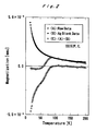
- FIG. 2 shows the change in magnetization with changing temperature, wherein (A) indicates directly observed numerical data plots, (B) indicates the blank data for the silver substrate, and (C) shows the net magnetization each obtained by subtracting the corresponding values of (B) from those of (A).
- the invention provides a method for producing a thin film of ribbon-like oxide high-Tc superconductor having a unique texture in which extremely thin ribbon- or tape-like thin films cross each other
- the method of the present invention greatly reduces the total production cost, because it not only considerably lowers the initial cost and running cost, but also enables mass production of thin films.
Landscapes
- Engineering & Computer Science (AREA)
- Manufacturing & Machinery (AREA)
- Inorganic Compounds Of Heavy Metals (AREA)
- Superconductors And Manufacturing Methods Therefor (AREA)
- Crystals, And After-Treatments Of Crystals (AREA)
- Superconductor Devices And Manufacturing Methods Thereof (AREA)
Description
- The invention of the present application relates to a method for producing a thin film of ribbon-like oxide high-temperature superconductor. In further detail, it relates to a method for producing thin film of ribbon-like oxide high-temperature (high-Tc) superconductor which can also be used as thin films of Bi-based oxide superconductors comprising a ribbon- or tape-like texture, useful for novel applications such as electronic devices.
- Thin films of Bi-based oxide superconductors has been produced heretofore by using vacuum evaporation techniques such as sputtering.
- However, the conventionally used methods above found difficulties in producing large area products. Moreover, these film production processes using the vacuum technology suffer problems such as a low mass-productivity and an increase in production cost because of the long duration of time required for evacuation within a single batch. Furthermore, a large equipment installation is required in the use of vacuum technology, and a high cost of operating the entire installation is another problem.
- Lang et al., "Influence of the maximum temperature during partial melt-processing of Bi-2212 thick films on microstructure and j"c, Physica C, vol. 294, 1998, pages 7-16 describes the preparation of samples involving placing samples of Bi2.2Sr2.05Ca95Cu2Ox and an additive on a silver substrate and heating to 886-930°C. The Bi-2212 of the films obtained are in grains or platelet-like form.
- In the light of the aforementioned circumstances, an object of the invention disclosed in the present application is to provide a novel method for producing superconducting thin films at a smaller initial cost and at a reduced running cost, which is yet capable of realizing high reproducibility and mass productivity.
- As a means for achieving the object above, the invention disclosed in the present application provides a method for producing a thin film of ribbon-like oxide high-temperature superconductor, which comprises:
- (a) placing a solid starting material for the oxide high-temperature superconductor at a predetermined position on a substrate, and
- (b) heating it at a temperature in the vicinity of the melting point of the solid starting material under ambient pressure in an oxygen atmosphere
- The present invention also provides the method described above, wherein the thin film of the ribbon-like oxide high-temperature superconductor that is produced by the method comprises a texture in which extremely thin ribbon- or tape-like thin films cross each other; wherein a powder or a sintered pellet of Bi-based oxide superconductor Bi2Sr2Cu2Ox, is used as the solid starting material, and the heat treatment is performed in the temperature range of from 850 to 913°C; wherein an amorphous material is used as the solid starting material, and the heat treatment is performed in the temperature range of from 800 to 890 °C;
or wherein silver or a silver-based alloy is used for the substrate. - The invention according to the present application is described by referring to embodiments.
- More specifically describing by way of an example, the invention according to the present application provides a production method capable of producing a unique oxide high To superconductor thin film having a texture as such that ribbon- or tape-like thin films cross each other, said method comprising placing a solid starting material for a Bi-based oxide superconductor on an edge of a substrate such as a silver substrate, etc., and performing a heat treatment in an oxygen atmosphere under ambient pressure by heating at a temperature of, for instance, 905 °C, followed by isothermal heating at 860 °C.
- In the present case, the heat treatment is performed, for instance, in the vicinity of the melting point (860 °C). The term "in the vicinity of" as referred herein is generally defined as a temperature range from 60 °C below to 60 °C over the melting point of the solid starting material. Specifically, considering the case of the Bi-based solid starting material as above wherein the melting point is 860 °C, the heat treatment is preferably performed in a temperature range of from 800 to 920 °C.
- A more preferred temperature range for the heat treatment can be set in accordance with the type and the composition of the solid starting material. In the case of using a powder or a sintered pellet corresponding to a Bi-2212 phase (Bi2Sr2Ca1Cu2Ox) as the solid starting material, a temperature range of from 850 to 913 °C is preferred, whereas a heat treatment in the temperature range of from 800 to 890 °C is preferable for a case using an amorphous material for the solid starting material.
- The consideration for the heat treatment in the vicinity of the melting point, which is performed in the temperature range of from 60 °C below to 60 °C above the melting point is not only applied to the Bi-Sr-Ca-Cu-Ox system composition, but is generally applied to various types of Bi-based oxide superconductors such as the Bi-Pb-Sr-Ca-Cu-Ox system. If the heat treatment should be performed at a temperature considerably higher than the melting point, the desired thin film would not be formed, but a thick film would result. If the temperature is too low, ribbon-like crystals cannot be obtained.
- The heat treatment is performed in an oxygen atmosphere under ambient pressure. A slightly reduced pressure state or a slightly pressurized state is also allowable to maintain the oxygen atmosphere. The oxygen atmosphere may be 100 % gaseous O2, or a mixed gas atmosphere containing gaseous O2 at a partial pressure of 80 % or higher accompanied by other inert gases such as gaseous N2 or a rare gas. If the partial pressure of O2 is less than 80 %, it becomes difficult to obtain ribbon-like crystals.
- Although there may be considered using various types of substrates, silver or a silver alloy can be exemplified as a representative material.
- In accordance with the method of the present invention, a super thin film having unique texture can be produced on the substrate. Thus, a novel application such as an electronic device taking advantage of this particular texture can be considered.
- The thin film provided by the method of the present invention can be characterized by a thin film consisting of fine ribbon-like oxide high Tc superconductors developed into a film-like shape. Furthermore, the ribbon-like oxide high Tc superconductors are extremely thin ribbon-like or tape-like films, and a large number of these ribbon- or tape-like thin films cross each other as to form a texture as a whole. The ribbon-like oxide high Tc superconductors are presumably crystalline, consisting of single crystals, or principally containing single crystals.
- Vacuum evaporation technology such as a sputtering process has been employed heretofore to produce the thin films of Bi-based oxide superconductors; however, the present invention enables the production of films under ambient pressure. Moreover, as compared with the vacuum technology which requires a large equipment installation, the only requirement in the present invention is an electric furnace. Thus, in practical application, the installation can be set up at an extremely low cost and yet, at a very simple structure and in a reduced floor area. This suppresses the operation cost to a low level.
- Furthermore, in contrast to the case of vacuum evaporation which was found difficult to produce large area products, the method according to the present invention readily enables mass production by arranging a plurality of samples inside the furnace. Further, as compared with the conventional filming methods using the vacuum technology, the mass productivity of the method according to the present invention is far improved because it provides thin films under ambient pressure and thereby eliminates the time necessary for vacuum evacuation.
-
-
FIG. 1 is an optical micrograph showing a specimen produced in the Example; and -
FIG. 2 is a diagram showing the relation between temperature and magnetization. - The constitution of the present invention as well as the function and the effect thereof are described in further detail below by making reference to the Example below. It should be understood, however, that the present invention is by no way limited thereto.
- A powder with a composition corresponding to Bi-2212 phase (Bi2Sr2Ca1cu2Ox) was placed on the edge of a silver substrate, and was heated for 10 minutes at 905 °C in pure gaseous oxygen under ambient pressure, followed by isothermal heating at 860 °C for 6 hours. As a result, numerous ribbon- or tape-like structures were observed to generate.
- The attached
FIG. 1 shows the optical micrograph of the specimen produced in the present Example. - Referring to
FIG. 1 , it was confirmed by the observation under an optical microscope that the texture consists of ribbon- or tape-like structures each several hundreds of micrometers in length, several tens of micrometers in width, and less than a micrometer in thickness. - The structure of the specimen was analyzed by X ray diffraction analysis, and the presence of a Bi-2212 texture having approximately a c-axis crystallographic orientation was confirmed. From the fact that no crystallite size was observed under a scanning electron microscope or an optical microscope, and because the manner of crystal growth strongly suggests the formation of single crystals, the texture was presumed to consist of single crystals.
- The superconductivity of the texture was evaluated by measuring the electric resistance using DC four-probe method, a sharp superconducting transition showing zero resistance was confirmed at ca. 75 K.
- The attached
FIG. 2 shows the change in magnetization with changing temperature, wherein (A) indicates directly observed numerical data plots, (B) indicates the blank data for the silver substrate, and (C) shows the net magnetization each obtained by subtracting the corresponding values of (B) from those of (A). - It can be seen from
FIG. 2 that a superconducting transition is observed at a temperature over ca. 80 K. - As compared with the values of a thin film specimen prepared by a general vacuum process, those obtained above are extremely high, and suggest the generation of a film of very high quality.
- As described above in detail, the invention according to the present application provides a method for producing a thin film of ribbon-like oxide high-Tc superconductor having a unique texture in which extremely thin ribbon- or tape-like thin films cross each other
- As compared with a conventional vacuum process, the method of the present invention greatly reduces the total production cost, because it not only considerably lowers the initial cost and running cost, but also enables mass production of thin films.
Claims (6)
- Method for producing a thin film of ribbon-like oxide high-temperature superconductor, which comprises(a) placing a solid starting material for the oxide high-temperature superconductor at a predetermined position on a substrate, and(b) heating it at a temperature in the vicinity of the melting point of the solid starting material under ambient pressure in an oxygen atmosphere,so as to form a thin film consisting of fine ribbon- like or tape-like crystalline oxide high-temperature superconductors developed into a film-like shape.
- A method as claimed in claim 1 wherein said solid starting material is in the form of powder or a sintered pellet.
- A method as claimed in claim 1, or claim 2 wherein the thin film of the ribbon-like oxide high-temperature superconductor conmprises a texture in which extremely thin ribbon- or tape-like thin films cross each other.
- A method as claimed in any of the preceding claims, wherein a powder or a sintered pellet of Bi-based oxide superconductor Bi2Sr2Ca1Cu2Ox is used as the solid starting material, and the heat treatment is performed in the temperature range of from 850 to 913°C.
- A method as claimed in any one of claims 1 to 3, wherein an amorphous material is used as the solid starting material, and the heat treatment is performed in the temperature range of from 800 to 890 °C.
- A method as claimed in any of claims 1 to 5, wherein silver or a silver-based alloy is used for the substrate.
Applications Claiming Priority (2)
| Application Number | Priority Date | Filing Date | Title |
|---|---|---|---|
| JP4911499 | 1999-02-25 | ||
| JP11049114A JP3086876B1 (en) | 1999-02-25 | 1999-02-25 | Method for producing thin film of ribbon-shaped oxide high-temperature superconductor |
Publications (3)
| Publication Number | Publication Date |
|---|---|
| EP1032055A2 EP1032055A2 (en) | 2000-08-30 |
| EP1032055A3 EP1032055A3 (en) | 2002-11-06 |
| EP1032055B1 true EP1032055B1 (en) | 2008-05-28 |
Family
ID=12822049
Family Applications (1)
| Application Number | Title | Priority Date | Filing Date |
|---|---|---|---|
| EP00301482A Expired - Lifetime EP1032055B1 (en) | 1999-02-25 | 2000-02-24 | Method for producing thin films of ribbon-like oxide high-temperature superconductor |
Country Status (4)
| Country | Link |
|---|---|
| US (1) | US6340657B1 (en) |
| EP (1) | EP1032055B1 (en) |
| JP (1) | JP3086876B1 (en) |
| DE (1) | DE60038997D1 (en) |
Families Citing this family (1)
| Publication number | Priority date | Publication date | Assignee | Title |
|---|---|---|---|---|
| US8592346B2 (en) | 2010-08-02 | 2013-11-26 | The Texas A&M University System | Textured powder wires |
Family Cites Families (2)
| Publication number | Priority date | Publication date | Assignee | Title |
|---|---|---|---|---|
| CH682358A5 (en) * | 1991-02-22 | 1993-08-31 | Asea Brown Boveri | Ceramic high temp. superconductor prodn. - by pouring starting material into mould, heating, cooling, thermally treating in oxygen@ and cooling, for shield magnetic fields in switching elements |
| US5856277A (en) * | 1996-06-03 | 1999-01-05 | Illinois Superconductor Corporation | Surface texturing of superconductors by controlled oxygen pressure |
-
1999
- 1999-02-25 JP JP11049114A patent/JP3086876B1/en not_active Expired - Lifetime
-
2000
- 2000-02-24 DE DE60038997T patent/DE60038997D1/en not_active Expired - Lifetime
- 2000-02-24 EP EP00301482A patent/EP1032055B1/en not_active Expired - Lifetime
- 2000-02-25 US US09/513,194 patent/US6340657B1/en not_active Expired - Lifetime
Also Published As
| Publication number | Publication date |
|---|---|
| DE60038997D1 (en) | 2008-07-10 |
| EP1032055A3 (en) | 2002-11-06 |
| JP3086876B1 (en) | 2000-09-11 |
| US6340657B1 (en) | 2002-01-22 |
| JP2000247794A (en) | 2000-09-12 |
| EP1032055A2 (en) | 2000-08-30 |
Similar Documents
| Publication | Publication Date | Title |
|---|---|---|
| US6226858B1 (en) | Method of manufacturing an oxide superconductor wire | |
| CA1330193C (en) | Method for making artificial layered high-t_ superconductors | |
| Macmanus‐Driscoll | Materials chemistry and thermodynamics of REBa2Cu3O7− x | |
| US5100866A (en) | Process for producing compound oxide high temperature superconducting material Tly Cul-y O3-z where RE=Y or La | |
| JPH08506216A (en) | Superconducting YBa formed at a low temperature. Lower 2 Cu Cu Lower 3 O Lower 7-x | |
| JP3089294B2 (en) | Manufacturing method of superconducting tape material | |
| US5206211A (en) | Process for the production of an elongate body consisting of longitudinally aligned acicular crystals of a superconducting material | |
| KR20050118294A (en) | Metal base plate for oxide superconductive wire rod, oxide superconductive wire rod and process for producing the same | |
| US6340657B1 (en) | Method for producing thin films of ribbon-like oxide high-temperature superconductor | |
| JP2920497B2 (en) | Manufacturing method of superconducting tape material | |
| CN1312332C (en) | Oxide high-temperature superconductor and its preparation method | |
| JPH02167820A (en) | Method for forming T1-based composite oxide superconductor thin film | |
| EP0450074B1 (en) | Method for preparing thin film of oxide superconductor and base used in the preparation | |
| CN1018311B (en) | Method for film forming of bismuth system complex oxide superconductive film | |
| EP0676817B1 (en) | Method of preparing high-temperature superconducting wire | |
| US5308800A (en) | Apparatus and method for forming textured bulk high temperature superconducting materials | |
| US5206214A (en) | Method of preparing thin film of superconductor | |
| JP3787572B2 (en) | Selective reduction type high temperature superconductor and method for producing the same | |
| CA2453922C (en) | Oxide high-critical temperature superconductor acicular crystal and method for producing the same | |
| JPS63301424A (en) | Manufacture of oxide superconductor membrane | |
| EP0516148A2 (en) | Oxide superconductive material and method of preparing the same | |
| JP4153651B2 (en) | Seed crystal of oxide superconducting material and manufacturing method of oxide superconducting material using the same | |
| JPH03275504A (en) | Oxide superconductor thin film and its production | |
| Wu | Epitaxy of Hg-Based High-T c Superconducting Thin Films | |
| JP2920496B2 (en) | Method of forming oxide dispersed particles |
Legal Events
| Date | Code | Title | Description |
|---|---|---|---|
| PUAI | Public reference made under article 153(3) epc to a published international application that has entered the european phase |
Free format text: ORIGINAL CODE: 0009012 |
|
| AK | Designated contracting states |
Kind code of ref document: A2 Designated state(s): AT BE CH CY DE DK ES FI FR GB GR IE IT LI LU MC NL PT SE |
|
| AX | Request for extension of the european patent |
Free format text: AL;LT;LV;MK;RO;SI |
|
| PUAL | Search report despatched |
Free format text: ORIGINAL CODE: 0009013 |
|
| AK | Designated contracting states |
Kind code of ref document: A3 Designated state(s): AT BE CH CY DE DK ES FI FR GB GR IE IT LI LU MC NL PT SE |
|
| AX | Request for extension of the european patent |
Free format text: AL;LT;LV;MK;RO;SI |
|
| 17P | Request for examination filed |
Effective date: 20030124 |
|
| AKX | Designation fees paid |
Designated state(s): DE FR NL |
|
| GRAP | Despatch of communication of intention to grant a patent |
Free format text: ORIGINAL CODE: EPIDOSNIGR1 |
|
| RIN1 | Information on inventor provided before grant (corrected) |
Inventor name: ARISAWA, SHUNICHI Inventor name: MIAO, HANPING Inventor name: HATANO, TAKESHI Inventor name: TOGANO, KAZUMASA |
|
| RAP1 | Party data changed (applicant data changed or rights of an application transferred) |
Owner name: JAPAN AS REPRESENTED BY DIRECTOR GENERAL OF NATION |
|
| GRAS | Grant fee paid |
Free format text: ORIGINAL CODE: EPIDOSNIGR3 |
|
| GRAA | (expected) grant |
Free format text: ORIGINAL CODE: 0009210 |
|
| AK | Designated contracting states |
Kind code of ref document: B1 Designated state(s): DE FR NL |
|
| REF | Corresponds to: |
Ref document number: 60038997 Country of ref document: DE Date of ref document: 20080710 Kind code of ref document: P |
|
| PLBE | No opposition filed within time limit |
Free format text: ORIGINAL CODE: 0009261 |
|
| STAA | Information on the status of an ep patent application or granted ep patent |
Free format text: STATUS: NO OPPOSITION FILED WITHIN TIME LIMIT |
|
| 26N | No opposition filed |
Effective date: 20090303 |
|
| PGFP | Annual fee paid to national office [announced via postgrant information from national office to epo] |
Ref country code: NL Payment date: 20110216 Year of fee payment: 12 Ref country code: DE Payment date: 20110218 Year of fee payment: 12 Ref country code: FR Payment date: 20110302 Year of fee payment: 12 |
|
| REG | Reference to a national code |
Ref country code: NL Ref legal event code: V1 Effective date: 20120901 |
|
| REG | Reference to a national code |
Ref country code: FR Ref legal event code: ST Effective date: 20121031 |
|
| REG | Reference to a national code |
Ref country code: DE Ref legal event code: R119 Ref document number: 60038997 Country of ref document: DE Effective date: 20120901 |
|
| PG25 | Lapsed in a contracting state [announced via postgrant information from national office to epo] |
Ref country code: NL Free format text: LAPSE BECAUSE OF NON-PAYMENT OF DUE FEES Effective date: 20120901 Ref country code: FR Free format text: LAPSE BECAUSE OF NON-PAYMENT OF DUE FEES Effective date: 20120229 |
|
| PG25 | Lapsed in a contracting state [announced via postgrant information from national office to epo] |
Ref country code: DE Free format text: LAPSE BECAUSE OF NON-PAYMENT OF DUE FEES Effective date: 20120901 |