EP1031132B1 - System and method for data planarization - Google Patents
System and method for data planarization Download PDFInfo
- Publication number
- EP1031132B1 EP1031132B1 EP98957901A EP98957901A EP1031132B1 EP 1031132 B1 EP1031132 B1 EP 1031132B1 EP 98957901 A EP98957901 A EP 98957901A EP 98957901 A EP98957901 A EP 98957901A EP 1031132 B1 EP1031132 B1 EP 1031132B1
- Authority
- EP
- European Patent Office
- Prior art keywords
- data
- bit
- data words
- storage bank
- bit data
- Prior art date
- Legal status (The legal status is an assumption and is not a legal conclusion. Google has not performed a legal analysis and makes no representation as to the accuracy of the status listed.)
- Expired - Lifetime
Links
Images


Classifications
-
- G—PHYSICS
- G09—EDUCATION; CRYPTOGRAPHY; DISPLAY; ADVERTISING; SEALS
- G09G—ARRANGEMENTS OR CIRCUITS FOR CONTROL OF INDICATING DEVICES USING STATIC MEANS TO PRESENT VARIABLE INFORMATION
- G09G3/00—Control arrangements or circuits, of interest only in connection with visual indicators other than cathode-ray tubes
- G09G3/20—Control arrangements or circuits, of interest only in connection with visual indicators other than cathode-ray tubes for presentation of an assembly of a number of characters, e.g. a page, by composing the assembly by combination of individual elements arranged in a matrix no fixed position being assigned to or needed to be assigned to the individual characters or partial characters
- G09G3/34—Control arrangements or circuits, of interest only in connection with visual indicators other than cathode-ray tubes for presentation of an assembly of a number of characters, e.g. a page, by composing the assembly by combination of individual elements arranged in a matrix no fixed position being assigned to or needed to be assigned to the individual characters or partial characters by control of light from an independent source
- G09G3/36—Control arrangements or circuits, of interest only in connection with visual indicators other than cathode-ray tubes for presentation of an assembly of a number of characters, e.g. a page, by composing the assembly by combination of individual elements arranged in a matrix no fixed position being assigned to or needed to be assigned to the individual characters or partial characters by control of light from an independent source using liquid crystals
- G09G3/3611—Control of matrices with row and column drivers
- G09G3/3648—Control of matrices with row and column drivers using an active matrix
-
- G—PHYSICS
- G09—EDUCATION; CRYPTOGRAPHY; DISPLAY; ADVERTISING; SEALS
- G09G—ARRANGEMENTS OR CIRCUITS FOR CONTROL OF INDICATING DEVICES USING STATIC MEANS TO PRESENT VARIABLE INFORMATION
- G09G3/00—Control arrangements or circuits, of interest only in connection with visual indicators other than cathode-ray tubes
- G09G3/20—Control arrangements or circuits, of interest only in connection with visual indicators other than cathode-ray tubes for presentation of an assembly of a number of characters, e.g. a page, by composing the assembly by combination of individual elements arranged in a matrix no fixed position being assigned to or needed to be assigned to the individual characters or partial characters
- G09G3/2007—Display of intermediate tones
- G09G3/2018—Display of intermediate tones by time modulation using two or more time intervals
Definitions
- the present invention relates to a data reformatter for reformatting display data associated with pixels in rows of a display according to the preamble of claim 1.
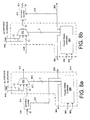
- the storage bank is a bi-directional shift register, including a clock input terminal, for receiving a data shift signal, and a direction terminal, for receiving a direction control signal.
- the bi-directional shift register includes a plurality of flip-flops and a plurality of multiplexers, each arranged in a rectangular array of columns and rows. Each of the flip-flops has a control terminal coupled to the clock terminal of the bi-directional shift register, an input terminal, and an output terminal.
- Each multiplexer has a first input terminal, a second input terminal, a control terminal coupled to the direction terminal of the bi-directional shift register, and an output terminal coupled to the input terminal of an associated one of the flip-flops.
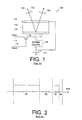
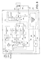
- driver 800 transfers the modified display data, via 32bit data output bus 824, along with control signals, via LCD control bus 826, to a micro-LCD 828, which includes an array of liquid crystal pixel cells, similar to the pixel cell shown in FIG.1 .
- Multiplexer 852 receives data from data bus 848, from 32-bit "force-on” bus 854, and from 32-bit "force-off” bus 856.
- Each line of force-on bus 854 is maintained at a voltage (Von) corresponding to an "on” state
- each line of force-off bus 856 is maintained at a voltage (Voff) corresponding to an "off' state.
- the sources of the forced state data asserted on force-on bus 854 and force-off bus 856 are system voltage reference terminals (e.g., Vdd and Ground). Those skilled in the art will understand, however, that alternate sources of forced state data, for example registers, may be employed.
- Bi-directional shift register 902 operates as follows. When input controller 802 asserts a first signal on DIR control line 832, all multiplexers 1004(r,c) couple their first input terminals 1006 with the inputs (D) of flip-flops 1002(r,c). Then, when the first clock signal is received via CLK line 834, flip-flops 1002(r,15) latch the 8-bit data word present on data input bus 816 onto their non-inverting (Q) outputs.
Landscapes
- Engineering & Computer Science (AREA)
- Chemical & Material Sciences (AREA)
- Crystallography & Structural Chemistry (AREA)
- Physics & Mathematics (AREA)
- Computer Hardware Design (AREA)
- General Physics & Mathematics (AREA)
- Theoretical Computer Science (AREA)
- Control Of Indicators Other Than Cathode Ray Tubes (AREA)
- Liquid Crystal Display Device Control (AREA)
- Communication Control (AREA)
Applications Claiming Priority (3)
| Application Number | Priority Date | Filing Date | Title |
|---|---|---|---|
| US970307 | 1978-12-18 | ||
| US08/970,307 US6144356A (en) | 1997-11-14 | 1997-11-14 | System and method for data planarization |
| PCT/US1998/024215 WO1999026225A1 (en) | 1997-11-14 | 1998-11-13 | System and method for data planarization |
Publications (2)
| Publication Number | Publication Date |
|---|---|
| EP1031132A1 EP1031132A1 (en) | 2000-08-30 |
| EP1031132B1 true EP1031132B1 (en) | 2011-03-16 |
Family
ID=25516737
Family Applications (1)
| Application Number | Title | Priority Date | Filing Date |
|---|---|---|---|
| EP98957901A Expired - Lifetime EP1031132B1 (en) | 1997-11-14 | 1998-11-13 | System and method for data planarization |
Country Status (8)
| Country | Link |
|---|---|
| US (1) | US6144356A (no) |
| EP (1) | EP1031132B1 (no) |
| JP (1) | JP2002537569A (no) |
| CN (1) | CN1136532C (no) |
| AT (1) | ATE502372T1 (no) |
| CA (1) | CA2309906C (no) |
| DE (1) | DE69842187D1 (no) |
| WO (1) | WO1999026225A1 (no) |
Families Citing this family (27)
| Publication number | Priority date | Publication date | Assignee | Title |
|---|---|---|---|---|
| US6803885B1 (en) | 1999-06-21 | 2004-10-12 | Silicon Display Incorporated | Method and system for displaying information using a transportable display chip |
| DE10121855A1 (de) * | 2001-05-04 | 2003-02-13 | Atmel Germany Gmbh | Verfahren zur Übertragung von Daten |
| GB0204410D0 (en) * | 2002-02-25 | 2002-04-10 | Bae Systems Plc | Weighgtless thermocoder |
| WO2004104790A2 (en) | 2003-05-20 | 2004-12-02 | Kagutech Ltd. | Digital backplane |
| JP4732709B2 (ja) * | 2004-05-20 | 2011-07-27 | 株式会社半導体エネルギー研究所 | シフトレジスタ及びそれを用いた電子機器 |
| US20060066645A1 (en) * | 2004-09-24 | 2006-03-30 | Ng Sunny Y | Method and apparatus for providing a pulse width modulation sequence in a liquid crystal display |
| US20060190704A1 (en) * | 2005-02-24 | 2006-08-24 | International Business Machines Corporation | Apparatus for increasing addressability of registers within a processor |
| US8339428B2 (en) * | 2005-06-16 | 2012-12-25 | Omnivision Technologies, Inc. | Asynchronous display driving scheme and display |
| US7884839B2 (en) * | 2005-12-05 | 2011-02-08 | Miradia Inc. | Method and system for image processing for spatial light modulators |
| US8223179B2 (en) * | 2007-07-27 | 2012-07-17 | Omnivision Technologies, Inc. | Display device and driving method based on the number of pixel rows in the display |
| TW200931380A (en) * | 2008-01-14 | 2009-07-16 | Ili Technology Corp | Data accessing system and data accessing method |
| US8228350B2 (en) * | 2008-06-06 | 2012-07-24 | Omnivision Technologies, Inc. | Data dependent drive scheme and display |
| US8228349B2 (en) * | 2008-06-06 | 2012-07-24 | Omnivision Technologies, Inc. | Data dependent drive scheme and display |
| US9024964B2 (en) * | 2008-06-06 | 2015-05-05 | Omnivision Technologies, Inc. | System and method for dithering video data |
| JP2011043766A (ja) * | 2009-08-24 | 2011-03-03 | Seiko Epson Corp | 変換回路、表示駆動回路、電気光学装置、及び電子機器 |
| US20130027416A1 (en) * | 2011-07-25 | 2013-01-31 | Karthikeyan Vaithianathan | Gather method and apparatus for media processing accelerators |
| US11030942B2 (en) | 2017-10-13 | 2021-06-08 | Jasper Display Corporation | Backplane adaptable to drive emissive pixel arrays of differing pitches |
| US10951875B2 (en) | 2018-07-03 | 2021-03-16 | Raxium, Inc. | Display processing circuitry |
| US11710445B2 (en) | 2019-01-24 | 2023-07-25 | Google Llc | Backplane configurations and operations |
| US11637219B2 (en) | 2019-04-12 | 2023-04-25 | Google Llc | Monolithic integration of different light emitting structures on a same substrate |
| US11238782B2 (en) | 2019-06-28 | 2022-02-01 | Jasper Display Corp. | Backplane for an array of emissive elements |
| US11626062B2 (en) | 2020-02-18 | 2023-04-11 | Google Llc | System and method for modulating an array of emissive elements |
| CN115362491A (zh) | 2020-04-06 | 2022-11-18 | 谷歌有限责任公司 | 显示组件 |
| US11538431B2 (en) | 2020-06-29 | 2022-12-27 | Google Llc | Larger backplane suitable for high speed applications |
| GB2598156B (en) | 2020-08-21 | 2023-05-31 | Dualitas Ltd | A spatial light modulator |
| US11978506B2 (en) | 2020-12-10 | 2024-05-07 | Agency For Science, Technology And Research | Spatial light modulator |
| CN117769738A (zh) | 2021-07-14 | 2024-03-26 | 谷歌有限责任公司 | 用于脉冲宽度调制的背板和方法 |
Citations (2)
| Publication number | Priority date | Publication date | Assignee | Title |
|---|---|---|---|---|
| US3204223A (en) * | 1957-11-25 | 1965-08-31 | Burroughs Corp | Magnetic core storage and transfer apparatus |
| US5325109A (en) * | 1990-12-27 | 1994-06-28 | Calcomp Inc. | Method and apparatus for manipulation of pixel data in computer graphics |
Family Cites Families (5)
| Publication number | Priority date | Publication date | Assignee | Title |
|---|---|---|---|---|
| CA2063744C (en) * | 1991-04-01 | 2002-10-08 | Paul M. Urbanus | Digital micromirror device architecture and timing for use in a pulse-width modulated display system |
| US5255100A (en) * | 1991-09-06 | 1993-10-19 | Texas Instruments Incorporated | Data formatter with orthogonal input/output and spatial reordering |
| JP3329008B2 (ja) * | 1993-06-25 | 2002-09-30 | ソニー株式会社 | 双方向信号伝送回路網及び双方向信号転送シフトレジスタ |
| EP0709822A3 (en) * | 1994-10-31 | 1996-07-31 | Texas Instruments Inc | Improvements in or in connection with a data formatting device and frame memories |
| EP0827129A3 (en) * | 1996-08-30 | 1999-08-11 | Texas Instruments Incorporated | Formatting and storing data for display systems using spatial light modulators |
-
1997
- 1997-11-14 US US08/970,307 patent/US6144356A/en not_active Expired - Lifetime
-
1998
- 1998-11-13 DE DE69842187T patent/DE69842187D1/de not_active Expired - Lifetime
- 1998-11-13 CA CA002309906A patent/CA2309906C/en not_active Expired - Lifetime
- 1998-11-13 JP JP2000521506A patent/JP2002537569A/ja active Pending
- 1998-11-13 EP EP98957901A patent/EP1031132B1/en not_active Expired - Lifetime
- 1998-11-13 WO PCT/US1998/024215 patent/WO1999026225A1/en active Application Filing
- 1998-11-13 CN CNB988131250A patent/CN1136532C/zh not_active Expired - Lifetime
- 1998-11-13 AT AT98957901T patent/ATE502372T1/de not_active IP Right Cessation
Patent Citations (2)
| Publication number | Priority date | Publication date | Assignee | Title |
|---|---|---|---|---|
| US3204223A (en) * | 1957-11-25 | 1965-08-31 | Burroughs Corp | Magnetic core storage and transfer apparatus |
| US5325109A (en) * | 1990-12-27 | 1994-06-28 | Calcomp Inc. | Method and apparatus for manipulation of pixel data in computer graphics |
Also Published As
| Publication number | Publication date |
|---|---|
| JP2002537569A (ja) | 2002-11-05 |
| CN1136532C (zh) | 2004-01-28 |
| WO1999026225A1 (en) | 1999-05-27 |
| EP1031132A1 (en) | 2000-08-30 |
| CA2309906A1 (en) | 1999-05-27 |
| DE69842187D1 (de) | 2011-04-28 |
| US6144356A (en) | 2000-11-07 |
| CN1285944A (zh) | 2001-02-28 |
| CA2309906C (en) | 2008-05-20 |
| ATE502372T1 (de) | 2011-04-15 |
Similar Documents
| Publication | Publication Date | Title |
|---|---|---|
| EP1031132B1 (en) | System and method for data planarization | |
| US6072452A (en) | System and method for using forced states to improve gray scale performance of a display | |
| US6151011A (en) | System and method for using compound data words to reduce the data phase difference between adjacent pixel electrodes | |
| US9305480B2 (en) | Liquid crystal display device | |
| USRE40973E1 (en) | Liquid crystal driver and liquid crystal display device using the same | |
| EP0861484B1 (en) | Lcd driver ic with pixel inversion operation | |
| US5307085A (en) | Display apparatus having shift register of reduced operating frequency | |
| EP0391655B1 (en) | A drive device for driving a matrix-type LCD apparatus | |
| US6356260B1 (en) | Method for reducing power and electromagnetic interference in conveying video data | |
| US7102610B2 (en) | Display system with frame buffer and power saving sequence | |
| US6762739B2 (en) | System and method for reducing the intensity output rise time in a liquid crystal display | |
| GB2409096A (en) | Liquid crystal display device having dummy channels and channel selection unit and method of driving the same | |
| US6326980B1 (en) | System and method for using compound data words in a field sequential display driving scheme | |
| US7492343B2 (en) | Liquid crystal display device | |
| CA2325028C (en) | Internal row sequencer for reducing bandwidth and peak current requirements in a display driver circuit | |
| US6771246B2 (en) | Data transmission method and apparatus for driving a display | |
| GB2418520A (en) | Liquid crystal display device with shift registers |
Legal Events
| Date | Code | Title | Description |
|---|---|---|---|
| PUAI | Public reference made under article 153(3) epc to a published international application that has entered the european phase |
Free format text: ORIGINAL CODE: 0009012 |
|
| 17P | Request for examination filed |
Effective date: 20000602 |
|
| AK | Designated contracting states |
Kind code of ref document: A1 Designated state(s): AT BE CH CY DE DK ES FI FR GB GR IE IT LI LU MC NL PT SE |
|
| RAP1 | Party data changed (applicant data changed or rights of an application transferred) |
Owner name: AURORA SYSTEMS, INC. |
|
| RAP1 | Party data changed (applicant data changed or rights of an application transferred) |
Owner name: AURORA SYSTEMS, INC. |
|
| 17Q | First examination report despatched |
Effective date: 20070412 |
|
| GRAP | Despatch of communication of intention to grant a patent |
Free format text: ORIGINAL CODE: EPIDOSNIGR1 |
|
| GRAS | Grant fee paid |
Free format text: ORIGINAL CODE: EPIDOSNIGR3 |
|
| GRAA | (expected) grant |
Free format text: ORIGINAL CODE: 0009210 |
|
| AK | Designated contracting states |
Kind code of ref document: B1 Designated state(s): AT BE CH CY DE DK ES FI FR GB GR IE IT LI LU MC NL PT SE |
|
| REG | Reference to a national code |
Ref country code: GB Ref legal event code: FG4D |
|
| REG | Reference to a national code |
Ref country code: CH Ref legal event code: EP |
|
| REG | Reference to a national code |
Ref country code: IE Ref legal event code: FG4D |
|
| REF | Corresponds to: |
Ref document number: 69842187 Country of ref document: DE Date of ref document: 20110428 Kind code of ref document: P |
|
| REG | Reference to a national code |
Ref country code: DE Ref legal event code: R096 Ref document number: 69842187 Country of ref document: DE Effective date: 20110428 |
|
| REG | Reference to a national code |
Ref country code: NL Ref legal event code: VDEP Effective date: 20110316 |
|
| PG25 | Lapsed in a contracting state [announced via postgrant information from national office to epo] |
Ref country code: ES Free format text: LAPSE BECAUSE OF FAILURE TO SUBMIT A TRANSLATION OF THE DESCRIPTION OR TO PAY THE FEE WITHIN THE PRESCRIBED TIME-LIMIT Effective date: 20110627 Ref country code: GR Free format text: LAPSE BECAUSE OF FAILURE TO SUBMIT A TRANSLATION OF THE DESCRIPTION OR TO PAY THE FEE WITHIN THE PRESCRIBED TIME-LIMIT Effective date: 20110617 Ref country code: SE Free format text: LAPSE BECAUSE OF FAILURE TO SUBMIT A TRANSLATION OF THE DESCRIPTION OR TO PAY THE FEE WITHIN THE PRESCRIBED TIME-LIMIT Effective date: 20110316 |
|
| PG25 | Lapsed in a contracting state [announced via postgrant information from national office to epo] |
Ref country code: CY Free format text: LAPSE BECAUSE OF FAILURE TO SUBMIT A TRANSLATION OF THE DESCRIPTION OR TO PAY THE FEE WITHIN THE PRESCRIBED TIME-LIMIT Effective date: 20110316 Ref country code: FI Free format text: LAPSE BECAUSE OF FAILURE TO SUBMIT A TRANSLATION OF THE DESCRIPTION OR TO PAY THE FEE WITHIN THE PRESCRIBED TIME-LIMIT Effective date: 20110316 Ref country code: AT Free format text: LAPSE BECAUSE OF FAILURE TO SUBMIT A TRANSLATION OF THE DESCRIPTION OR TO PAY THE FEE WITHIN THE PRESCRIBED TIME-LIMIT Effective date: 20110316 |
|
| PG25 | Lapsed in a contracting state [announced via postgrant information from national office to epo] |
Ref country code: BE Free format text: LAPSE BECAUSE OF FAILURE TO SUBMIT A TRANSLATION OF THE DESCRIPTION OR TO PAY THE FEE WITHIN THE PRESCRIBED TIME-LIMIT Effective date: 20110316 |
|
| PG25 | Lapsed in a contracting state [announced via postgrant information from national office to epo] |
Ref country code: PT Free format text: LAPSE BECAUSE OF FAILURE TO SUBMIT A TRANSLATION OF THE DESCRIPTION OR TO PAY THE FEE WITHIN THE PRESCRIBED TIME-LIMIT Effective date: 20110718 |
|
| PG25 | Lapsed in a contracting state [announced via postgrant information from national office to epo] |
Ref country code: NL Free format text: LAPSE BECAUSE OF FAILURE TO SUBMIT A TRANSLATION OF THE DESCRIPTION OR TO PAY THE FEE WITHIN THE PRESCRIBED TIME-LIMIT Effective date: 20110316 |
|
| PLBE | No opposition filed within time limit |
Free format text: ORIGINAL CODE: 0009261 |
|
| STAA | Information on the status of an ep patent application or granted ep patent |
Free format text: STATUS: NO OPPOSITION FILED WITHIN TIME LIMIT |
|
| 26N | No opposition filed |
Effective date: 20111219 |
|
| PG25 | Lapsed in a contracting state [announced via postgrant information from national office to epo] |
Ref country code: DK Free format text: LAPSE BECAUSE OF FAILURE TO SUBMIT A TRANSLATION OF THE DESCRIPTION OR TO PAY THE FEE WITHIN THE PRESCRIBED TIME-LIMIT Effective date: 20110316 |
|
| REG | Reference to a national code |
Ref country code: DE Ref legal event code: R097 Ref document number: 69842187 Country of ref document: DE Effective date: 20111219 |
|
| PG25 | Lapsed in a contracting state [announced via postgrant information from national office to epo] |
Ref country code: IT Free format text: LAPSE BECAUSE OF FAILURE TO SUBMIT A TRANSLATION OF THE DESCRIPTION OR TO PAY THE FEE WITHIN THE PRESCRIBED TIME-LIMIT Effective date: 20110316 |
|
| PG25 | Lapsed in a contracting state [announced via postgrant information from national office to epo] |
Ref country code: MC Free format text: LAPSE BECAUSE OF NON-PAYMENT OF DUE FEES Effective date: 20111130 |
|
| REG | Reference to a national code |
Ref country code: CH Ref legal event code: PL |
|
| PG25 | Lapsed in a contracting state [announced via postgrant information from national office to epo] |
Ref country code: CH Free format text: LAPSE BECAUSE OF NON-PAYMENT OF DUE FEES Effective date: 20111130 Ref country code: LI Free format text: LAPSE BECAUSE OF NON-PAYMENT OF DUE FEES Effective date: 20111130 |
|
| REG | Reference to a national code |
Ref country code: IE Ref legal event code: MM4A |
|
| PG25 | Lapsed in a contracting state [announced via postgrant information from national office to epo] |
Ref country code: IE Free format text: LAPSE BECAUSE OF NON-PAYMENT OF DUE FEES Effective date: 20111113 |
|
| PG25 | Lapsed in a contracting state [announced via postgrant information from national office to epo] |
Ref country code: LU Free format text: LAPSE BECAUSE OF NON-PAYMENT OF DUE FEES Effective date: 20111113 |
|
| REG | Reference to a national code |
Ref country code: FR Ref legal event code: PLFP Year of fee payment: 18 |
|
| REG | Reference to a national code |
Ref country code: FR Ref legal event code: PLFP Year of fee payment: 19 |
|
| REG | Reference to a national code |
Ref country code: FR Ref legal event code: PLFP Year of fee payment: 20 |
|
| PGFP | Annual fee paid to national office [announced via postgrant information from national office to epo] |
Ref country code: DE Payment date: 20171130 Year of fee payment: 20 Ref country code: FR Payment date: 20171018 Year of fee payment: 20 |
|
| PGFP | Annual fee paid to national office [announced via postgrant information from national office to epo] |
Ref country code: GB Payment date: 20171026 Year of fee payment: 20 |
|
| REG | Reference to a national code |
Ref country code: DE Ref legal event code: R071 Ref document number: 69842187 Country of ref document: DE |
|
| REG | Reference to a national code |
Ref country code: GB Ref legal event code: PE20 Expiry date: 20181112 |
|
| PG25 | Lapsed in a contracting state [announced via postgrant information from national office to epo] |
Ref country code: GB Free format text: LAPSE BECAUSE OF EXPIRATION OF PROTECTION Effective date: 20181112 |