EP1030441A2 - Feedforward amplifier - Google Patents
Feedforward amplifier Download PDFInfo
- Publication number
- EP1030441A2 EP1030441A2 EP00103060A EP00103060A EP1030441A2 EP 1030441 A2 EP1030441 A2 EP 1030441A2 EP 00103060 A EP00103060 A EP 00103060A EP 00103060 A EP00103060 A EP 00103060A EP 1030441 A2 EP1030441 A2 EP 1030441A2
- Authority
- EP
- European Patent Office
- Prior art keywords
- amplifier
- output signal
- output
- signal
- signals
- Prior art date
- Legal status (The legal status is an assumption and is not a legal conclusion. Google has not performed a legal analysis and makes no representation as to the accuracy of the status listed.)
- Ceased
Links
Images


Classifications
-
- H—ELECTRICITY
- H03—ELECTRONIC CIRCUITRY
- H03F—AMPLIFIERS
- H03F1/00—Details of amplifiers with only discharge tubes, only semiconductor devices or only unspecified devices as amplifying elements
- H03F1/32—Modifications of amplifiers to reduce non-linear distortion
- H03F1/3223—Modifications of amplifiers to reduce non-linear distortion using feed-forward
- H03F1/3229—Modifications of amplifiers to reduce non-linear distortion using feed-forward using a loop for error extraction and another loop for error subtraction
Definitions
- the present invention relates to a feedforward amplifier which is mainly used in a device of a base station of a mobile communication system.
- a device of a base station of a mobile communication system is requested to be provided with a power amplifier which is excellent both in efficiency and linearity.
- the linearity is realized by performing distortion compensation according to the feedforward system.
- a feedforward amplifier is described by, for example, John L. B. Walker, "High-Power GaAs FET Amplifiers," Artech House, 1993, p.p. 332 to 333.
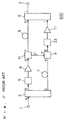
- Fig. 7 is a diagram showing an example of the configuration of a feedforward amplifier of the conventional art.
- a feedforward amplifier 600 an input terminal 1 allows an external signal to be input to the feedforward amplifier 600.
- An output terminal 2 allows a signal to be output from the feedforward amplifier 600 to the external.
- a power divider 3 divides the input from the input terminal 1 into two signals, and supplies the signals to a vector adjuster 5, and a delay circuit 7 of a coaxial cable, respectively.
- a main amplifier 6 amplifies an input from the vector adjuster 5.
- Directional coupler 51 receives the output of the main amplifier 6 outputs almost signals to delay circuit 9 from main port and outputs few signals to after-mentioned power combiner 8 from couple port.
- the power combiner 8 receives the output from the couple port of the directional coupler 51 and the output of the delay circuit 7 and outputs signals to a vector adjuster 33.
- An error amplifier 71 amplifies an input from the vector adjuster 33.
- a power combiner 4 combines inputs from the delay circuit 9 and the error amplifier 33 with each other and supplies the resulting signal to the output terminal 2.
- the characters a to j.e' and f' attached to the power divider 3, the power combiner 4, directional coupler 51 and the power combiner 8 indicate signal input/output ports of the devices, respectively.
- an input signal which is input via the input terminal 1 and contains multi-channel components is divided into two signals by the power divider 3.
- One of the two divided signals is amplified by the main amplifier 6 via the vector adjuster 5.
- the signal which contains distortion components is generated.
- the signal which is amplified by the main amplifer 6, is supplied to input port d of the directional coupler 51, and almost signal are output from the output port f and a few signal is output from the output port f' to be supplied to the input port e' of the power combiner 8.
- the other of the two divided signals is input to the input port e of the power combiner 8, via the delay circuit 7.
- the signal which is output from the output port f and contains the input signal components and the distortion components is input to the input port h of the power combiner 4 via the delay circuit 9.
- the distortion component signal output from the output port g is amplified by the error amplifier 71 via the vector adjuster 33, and the amplified signal is input to the input port i of the power combiner 4.
- the vector adjuster 33 and the delay circuit 9 are adjusted so that the distortion components of the input signals at the input ports h and i have the equal amplitude and opposite phases, a signal in which the distortion components are canceled each other and which contains only the input signal components can be obtained from the output terminal 2.
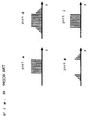
- Fig. 8 shows frequency spectra of the signals at the ports a, d, g and j of Fig. 7.
- the feedforward amplifier of the conventional art has the following problems.
- a first problem is as follows.
- the band of the error amplifier 71 in order to suppress the distortion component produced in the main amplifier 6 in a broader frequency band, the band of the error amplifier 71 must be broadened.
- distortion components produced in a region very close to the channel band can be sufficiently suppressed, therefore, there arises a problem in that those produced in a region of the band edge are more hardly suppressed.
- the configuration of the conventional art has a second problem in that the power consumption of the main amplifier 6 is large.
- a class A amplifier is usually used as the main amplifier 6. This means that the main amplifier produces lower distortion, but is lower in power efficiency and consumes a large power.
- a third problem is as follows.
- Each of delay elements used in the delay circuits 7 and 9 is configured by, for example, winding a coaxial cable in a spiral form.
- the cable is required to have a length of about 3 m. Therefore, there is a problem in that the delay elements occupy a large space and, in the case of a large power output, a large loss is caused by the power passing therethrough.
- the feedforward amplifier is configured in the following manner.
- a feedforward amplifier of the first present invention (corresponding to claim 1) comprises:
- a feedforward amplifier of the second present invention (corresponding to claim 2) according to the first present invention is such amplifier that said broadband auxiliary amplifier block comprises:
- the feedforward amplifier is configured in the following manner.
- a feedforward amplifier of the third present invention (corresponding to claim 3) comprises:
- a feedforward amplifier of the fourth present invention (correspondig to claim 4) according to the present third invention is such amplifier that said main amplifier is a class AB power amplifier.
- This configuration can attain an effect that the power efficiency can be improved, in addition to the above-mentioned effects.
- a feedforward amplifier of the fifth present invention (corresponding to claim 5) according to the third or fourth present invention is such amplifier that a band-pass filter which allows only a signal of an objective frequency to pass through said filter is disposed at an output end of said power combiner.
- This configuration can attain an effect that distortion which cannot be sufficiently canceled by a feedforward circuit can be canceled, in addition to the above-mentioned effects.
- a feedforward amplifier of the sixth present invention (corresponding to claim 6) according to the present third or fourth invention) is such amplifier that said second delay circuit functions also as a band-pass filter, a band-pass filter is disposed between said power combiner and said second vector adjuster, and distortion components which cannot be canceled by a feedforward function are canceled by a function of said band-pass filters.
- This configuration can attain an effect that distortion which cannot be sufficiently canceled by a feedforward circuit can be canceled, in addition to the above-mentioned effects.
- a feedforward amplifier of the present seventh invention (corresponding to claim 7) comprises:
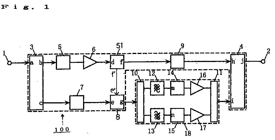
- Fig. 1 is a diagram of a feedforward amplifier which is an embodiment according to the first and second aspects of the invention.
- a feedforward amplifier 100 an input terminal 1 allows an external signal to be input to the feedforward amplifier 100.
- An output terminal 2 allows a signal to be output from the feedforward amplifier 100 to the external.
- a power divider 3 divides the input from the input terminal 1 into two signals, and supplies the signals to a vector adjuster 5 and a delay circuit 7, respectively.
- a main amplifier 6 amplifies an input from the vector adjuster 5.
- a directional coupler 51 is such means for receiving signal from the main amplifier 6 and ouputting almost signals to delay circuit 7 from the main port and outputting a few signals to the after-mentioned power combiner 8.
- a power combiner 8 receives inputs from the couple port of the directional coupler 51 and from the delay circuit 7 and outputs signals to a broadband auxiliary amplifier block 18.
- a power combiner 4 combines inputs from the delay circuit 9 and the broadband auxiliary amplifier block 18 with each other and supplies the resulting signal to the output terminal 2.
- the characters a to j, e, f' attached to the power divider 3, the power combiner 4, directional coupler 51 and the power combiner 8 indicate signal input/output ports of the devices, respectively.
- a power divider 10 divides an input from the output port g of the power combiner 8 into two signals, and supplies the signals to a low-pass filter 12, and a high-pass filter 13, respectively.
- the low-pass filter 12 allows only components of the input signal which have a lower frequency, to pass therethrough, and the high-pass filter 13 allows only those of the input signal which have a higher frequency, to pass therethrough.
- Vector adjusters 14 and 15 operate in the same manner as those of the prior art.
- error amplifiers 16 and 17 amplify distortion components.
- a power combiner 11 combines inputs from the error amplifiers 16 and 17 with each other and supplies the resulting signal to the input port i of the power combiner 4.
- the characters m and n attached to the vector adjusters 14 and 15 indicate signal input ports, respectively.
- an input signal which is input via the input terminal 1 and contains multi-channel components is divided into two signals by the power divider 3.
- One of the two divided signals is amplified by the main amplifier 6 via the vector adjuster 5.
- the other signal which is amplified by the main amplifer 6, is supplied to input port d of the directional coupler 51, and almost signal are output from the output port f and a few signal is output from the output port f' to be supplied to the input port e' of the power combiner 8.
- the other of the two divided signals is input to the input port e of the power combiner 8, via the delay circuit 7.
- the signal which is output from the output port f and contains the input signal components and the distortion components is input to the input port h of the power combiner 4 via the delay circuit 9.
- the distortion component signal output from the output port g is divided into two signals by the power divider 10.
- FIG. 2 (a) to (f) are views respectively showing frequency spectra of the signals at the input/output ports a, d, g, m, n, and j shown in Fig. 1.
- the error amplifier 16 amplifies the distortion components of the lower frequency band with respect to the channel band
- the error amplifier 17 amplifies those of the higher frequency band with respect to the channel band.
- the operation frequency band of the feedforward amplifier can be made excellent over a broad band.
- the broadband auxiliary amplifier block is configured so that distortion components of an input signal are divided into two frequency bands, and the divided distortion components are respectively amplified by the two error amplifiers.
- three or more band-pass filters may be disposed so that distortion components are divided into three or more frequency bands, and the divided distortion components are respectively amplified by three or more error amplifiers.
- the operation frequency band of the feedforward amplifier can be made broader.
- an error amplifier is configured to operate in parallel by a first error amplifier which amplifies distortion components of the lower frequency side with respect to the channel band, and a second error amplifier which amplifies distortion components of the higher frequency side with respect to the channel band, whereby the frequency band of the feedforward amplifier can be broadened.
- the above-described invention relates to the first and second aspects of the invention which have been mentioned in the Summary section. Next, the third to seventh aspects of the invention which have been mentioned in the SUMMARY section will be described.
- an input terminal 31 is connected to a port a of a power divider 32.
- a port b of the power divider 32 is connected to a main amplifier 34 which amplifies an input signal, via a vector adjuster 33 which adjusts the phase and the amplitude of a signal.
- the main amplifier 34 is connected to a port d of a directional coupler 51.
- the directional coupler 51 outputs almost inputted signals to port f and outputs a few inputted signals to port f'.
- a port c of the power divider 32 is connected to a port e of the power combiner 35 via a delay filter 36.
- the delay filter 36 is configured by two parallel-resonant circuits which are capacitively coupled to each other as illustrated, and delays a signal passing therethrough.
- the parallel-resonant circuits can be realized by a strip line.
- the port f' is connected to a port e' of the power combiner 8.
- the power combiner 35 receives signals from the port e, and e' and outputs the combined signals outsides from port g.
- the port f of the directional coupler 51 is connected to a port h of a power combiner 38 via a second delay filter 37 which is configured in the same manner as the delay filter 36.
- the port g of the power combiner 35 is connected to a port i of the power combiner 38, via a series circuit of a vector adjuster 39 which adjusts the phase and the amplitude of a signal, and an error amplifier 410.
- a port j of the power combiner 38 is connected to an output terminal 412 via a band-pass filter 411 which allows a frequency band of an objective signal to pass therethrough.
- Each of the delay filters 36 and 37 is a kind of band-pass filter, and designed with placing emphasis on the delaying characteristics rather than on the band passing characteristics.
- the band-pass filter 411 is designed with placing emphasis on the band passing characteristics rather than on the delaying characteristics.
- a feedforward unit 420 which is enclosed by a broken line is used as a unit in the case where plural feedforward amplifiers are operated in parallel as described in the following embodiment.
- an input signal which is input via the input terminal 31 and contains multi-channel components is input to the port a of the power divider 32 to be divided into two signals thereby.
- One of the two output signals is supplied from the port b to be adjusted in phase and amplitude by the vector adjuster 33, and then input to the main amplifier 34.
- the signal is power amplified by the amplifier 34, and the amplified signal is input to the port d of the directional coupler 51.
- the almost signals supplied to the port d of the directinal coupler 51 is output from port f and a few signals are output from port f' to be received by the port e' of the power combiner 35.
- the other of the two divided signals is output from the port c to be delayed by the delay filter 36, and the delayed signal is input to the port e of the power combiner 35.
- the delay by the delay filter 36 is set so as to be substantially equal in degree to that by the main amplifier 34.
- the vector adjuster 33 and the delay filter 36 are previously adjusted so that the input signal components of the input signals to the ports e and e' have the equal amplitude and opposite phases. Thus a signal in which the input signal components are canceled each other and which contains only the distortion components is output from the port g.
- the delay by the vector adjuster 33 is set to be large, so that the phase of the input signal via the port e' becomes opposite to that of the input signal via the port e.
- the vector adjuster 33 finely adjusts the phases to make the input signal via the port e' in phase with the input signal via the port e, and, in the directional coupler 51 and the power combiner 35, an addition is then performed while making the phase of the input signal via the port e' opposite to that of the input signal via the port e.
- the signal which is output from the output port f and contains the input signal components and the distortion components is delayed by the delay filter 37, and the delayed signal is input to the port h of the power combiner 38.
- the distortion component signal output from the port g is adjusted in phase and amplitude by the vector adjuster 39, and then amplified by the error amplifier 410.
- the amplified signal is input to the port i of the power combiner 38.
- the vector adjuster 39, the error amplifier 410, and the delay filter 37 are adjusted so that the distortion components of the input signals to the input ports h and i have the equal amplitude and opposite phases. As a result, a signal in which the distortion components are canceled each other and which contains only the input signal components should be output from the port j. Also in this case, the delay by the delay filter 37 is set so as to be substantially equal in degree to that by the error amplifier 410, and the delay by the vector adjuster 39 is set to be large, so that distortion components of the input signal to the port h, and the distortion signal to the port i are input with being opposite in phase to each other.
- the vector adjuster 39 performs only fine adjustment of the phase, and, in the power combiner 38, an addition is then performed while making the input distortion components via the port h opposite in phase to those via the port i. As a result, a signal in which the distortion components are canceled is output from the port j.
- the main amplifier 34 is configured by a class AB amplifier in order to enhance the efficiency, and hence intermodulation distortion is larger as compared with the case of a class A amplifier. Therefore, the signal output from the port j remains to contain distortion components of the outer side band that has been discussed in the Related Art section.
- the band-pass filter 411 is inserted between the port j of the power combiner 38 and the output terminal 412, whereby only the objective signal is allowed to pass through the filter, so that all of distortion components due to intermodulation are canceled and distortion is lowered to a level at which there arises no problem.
- the use of a delay filter in place of a delay circuit remarkably reduces the volume of the element, and that of a class AB amplifier as the main amplifier improves the power efficiency of the amplifier to reduce the power consumption.
- the increased portion of intermodulation distortion is suppressed by the band-pass filter.
- the delay filter 37 Especially as to the delay filter 37 , the signal which has been power amplified by the main amplifier 34 passes through the delay filter 37 and the delay filter 37 can attain not only an effect that the volume is reduced by the use of the delay filter 37 as compared with the conventional case where a coaxial delay circuit is used, but also an effect that the loss with respect to the passing signal can be reduced.
- the delay filter 37 should have preference to the delay filter 36.
- Fig. 4 is a diagram showing the circuit configuration of the embodiment.
- the embodiment is different from that of Fig. 3 in that the band-pass filter 411 is not disposed and the delay filter 37 has a band-pass filter function in addition to the delay function, and also that a band-pass filter 52 is connected between the port g and the vector adjuster 39.
- the signal input to the port h is a signal in which distortion components of the outer side band that has been discussed in the Related Art section are canceled.
- the output k from the band-pass filter 52 is a signal which contains distortion components but in which distortion components of the outer side are canceled.
- the signal which is combined by the power combiner 38 is a signal in which distortion components are canceled.
- Fig. 6 is a block diagram of the feedforward amplifier.
- two feedforward units are used so that, even when one of the units becomes faulty, the amplifier can continue to operate by using the other unit.
- An input terminal 21 is connected to a Wilkinson power divider 22.
- the Wilkinson power divider 22 has: quarter-wavelength lines 23 and 24 corresponding to a quarter of the wavelength of a signal of the frequency which is to be amplified; and an absorbing resistor 25.
- the each ends of lines 23 and 24 are connected to the input terminal 21, and the other ends of the lines are connected to the ends of the absorbing resistor 25, respectively.
- the ends of the absorbing resistor 25 are connected to input ends of mutually-independent feedforward units 20a and 20b.
- Each of the feedforward units 20a and 20b is identical with the feedforward unit 420 of Fig. 3.
- Output terminals of the feedforward units are connected to a Wilkinson power combiner 26.
- the Wilkinson power combiner 26 has an absorbing resistor 27, and quarter-wavelength lines 28 and 29 which are connected to the ends of the resistor, respectively.
- the other ends of the quarter-wavelength lines 28 and 29 are connected to one end of a band-pass filter 300, and the other end of the band-pass filter 300 is connected to an output terminal 310.
- the band-pass filter 411 of Fig. 3 may be added to the configuration in which the band-pass filter 300 exists. It is a matter of course that each of the feedforward units 20a and 20b may be identical with the feedforward unit of Fig. 4.
- the two feedforward units are used.
- further quarter-wavelength lines and absorbing resistors may be added to the Wilkinson power divider and combiner, and three or more feedforward units may be combinedly used.
- a Wilkinson power divider and a Wilkinson power combiner are described in detail by, for example, KONISHI Yoshihiro "KOSHUHA ⁇ MICROWAVE KAIRO NO KOSEIHO," June 20, 1993, p.p. 134 to 135, SOGO DENSHI SHUPPANSHA.
- the Wilkinson power divider 22 divides the input from the input terminal 21 into two signals, and the signals are respectively amplified by the feedforward units 20a and 20b to be reduced with distortion. Thereafter, the powers of the signals are combined with each other by the Wilkinson power combiner 26, and distortion components outside the signal band are canceled by the band-pass filter 300. The resulting signal is supplied to the output terminal 310.
- a case where one of the feedforward units 20a and 20b, e.g., the unit 20b becomes faulty will be considered.
- an influence due to the input terminal of the faulty feedforward unit 20b can be made substantially negligible by the absorbing resistor 25.
- an influence due to the output terminal of the faulty feedforward unit 20b can be made substantially negligible by the absorbing resistor 27. Although the output is reduced, therefore, the total system can continue to operate.
- an input signal is divided into plural signals by the Wilkinson power divider, the signals are amplified by using plural feedforward units according to the above-described embodiment, outputs of the units are combined with one another by the Wilkinson power combiner, and produced distortion is canceled by the band-pass filter, whereby a feedforward amplifier can be provided which can produce a high output power while consuming a small power, which, even when any one of the feedforward units is faulty, can continue to operate, and which is small in size and operates with a high efficiency.
- the volume of the feedforward amplifier according to the third to seventh aspects of the invention can be remarkably reduced.
- the feedforward amplifier can continue to operate while only the output power is reduced, even when any one of the feedforward units becomes faulty during operation. Therefore, the reliability of a system can be enhanced.
Landscapes
- Physics & Mathematics (AREA)
- Nonlinear Science (AREA)
- Engineering & Computer Science (AREA)
- Power Engineering (AREA)
- Amplifiers (AREA)
Abstract
Description
- 1
- input terminal
- 2
- output terminal
- 3, 10
- power divider
- 4,
- power combiner
- 5, 14, 15
- vector adjuster
- 6,
- main amplifier
- 7, 9,
- delay circuit
- 8,
- power combiner
- 11
- power combiner
- 12
- low-pass filter
- 13
- high-pass filter
- 16, 17, 71
- error amplifier
- 18
- broadband auxiliary amplifier block
- 100, 600
- feedforward amplifier
- 31, 21
- input terminal
- 32
- power divider
- 33, 39
- vector adjuster
- 34
- main amplifier
- 35
- power combiner
- 36, 37
- delay filter
- 38
- power combiner
- 410
- error amplifier
- 411, 300
- band-pass filter
- 412, 310
- output terminal
- 420, 20a, 20b
- feedforward unit
- 22
- Wilkinson power divider
- 23, 24, 28, 29
- quarter-wavelength line
- 25, 27
- absorbing resistor
- 26
- Wilkinson power combiner
- 51
- directional coupler
- 52
- band-pass filter
Claims (7)
- A feedforward amplifier comprising:a first power divider which divides an input signal into two signals;a first vector adjuster which adjusts an amplitude and a phase of one of output signals which are divided by said first power divider;a main amplifier which amplifies an output signal of said first vector adjuster;a first delay circuit which delays another output signals which are divided by said first power divider;a directional coupler which receives an output signal of said main amplifier and an output signal of said first delay circuit, and has a main port for outputting almost signals from the main amplifier and a couple port for outputting a few signals from the main amplifier;a power combiner which receives an output signal of said couple port and an output signal of said first delay circuit,to output a combined signals thereof;a second delay circuit which delays an output signal from said main port of said directional coupler;an auxiliary amplifier block which amplifies an output signal from said power combiner; anda power combiner which outputs a combined signal of an output signal of said second delay circuit, and an output signal of said auxiliary amplifier block,said auxiliary amplifier block beinga broadband auxiliary amplifier block having at least two error amplifiers which amplify the output signal from said power combiner while splitting the output signal into respective frequency bands that do not overlap with each other.
- A feedforward amplifier according to claim 1, wherein said broadband auxiliary amplifier block comprises:a power divider which divides the output signal from said power combiner, into two signals;a low-pass filter which allows a lower frequency component of one of output signals of said power divider;a first vector adjuster which adjusts an amplitude and a phase of an output signal of said low-pass filter;a first error amplifier which amplifies an output signal of said first vector adjuster;a high-pass filter which allows a higher frequency component of another one of the output signals of said power divider;a second vector adjuster which adjusts an amplitude and a phase of an output signal of said high-pass filter;a second error amplifier which amplifies an output signal of said second vector adjuster; anda power combiner which outputs a combined signal of an output signal of said first error amplifier and an output signal of said second error amplifier, to said power combiner.
- A feedforward amplifier comprising:a power divider which divides an input signal into two signals;a first vector adjuster which adjusts an amplitude and a phase of one of two output signals of said power divider;a main amplifier for amplifying an output of said first vector adjuster;a first delay circuit which delays another output signal of said power divider;a directional coupler which receives an output signal of said main amplifier and an output signal of said first delay circuit, and has a main port for outputting almost signals from the main amplifier and a couple port for outputting a few signals from the main amplifier;a power combiner which receives an output signal of said couple port and an output signal of said first delay circuit,to output a combined signals thereof;a second delay circuit which delays the output of said main port of the directional coupler;a second vector adjuster which adjusts an amplitude and a phase of an output signal of said power combiner;an error amplifier which amplifies an output signal of said second vector adjuster; anda power combiner which combines an output signal of said second delay circuit with an output of said error amplifier, to ooutput a combined signal;said first vector adjuster and said first delay circuit being adjusted so that, in said power combiner objective signal components are canceled and only distortion components are contained,said second vector adjuster and said second delay circuit being adjusted so that, in a combined signal output from said power combiner, distortion components are canceled and only objective signal components are contained,at least said second delay circuit being configured by a filter having phase delaying characteristics.
- A feedforward amplifier according to claim 3, wherein said main amplifier is a class AB power amplifier.
- A feedforward amplifier according to claim 3 or 4, wherein a band-pass filter which allows only a signal of an objective frequency to pass through said filter is disposed at an output end of said power combiner.
- A feedforward amplifier according to claim 3 or 4, wherein said second delay circuit functions also as a band-pass filter, a band-pass filter is disposed between said power combiner and said second vector adjuster, and distortion components which cannot be canceled by a feedforward function are canceled by a function of said band-pass filters.
- A feedforward amplifier comprising:a divider which divides an input signal into outputs of plural systems;plural feedforward amplifiers according to any one of claims 3 to 6, said amplifiers receiving the plural divided outputs of said divider, respectively, and amplifying the output;a combiner which combines outputs of said plural feedforward amplifiers with one another; anda band-pass filter which is connected to an output end of said combiner, and which allows only a signal of an objective frequency to pass said filter.
Applications Claiming Priority (4)
| Application Number | Priority Date | Filing Date | Title |
|---|---|---|---|
| JP11036708A JP2000236222A (en) | 1999-02-16 | 1999-02-16 | Feed forward amplifier |
| JP3670899 | 1999-02-16 | ||
| JP11046220A JP2000244253A (en) | 1999-02-24 | 1999-02-24 | Feed forward amplifier |
| JP4622099 | 1999-02-24 |
Publications (2)
| Publication Number | Publication Date |
|---|---|
| EP1030441A2 true EP1030441A2 (en) | 2000-08-23 |
| EP1030441A3 EP1030441A3 (en) | 2004-03-17 |
Family
ID=26375790
Family Applications (1)
| Application Number | Title | Priority Date | Filing Date |
|---|---|---|---|
| EP00103060A Ceased EP1030441A3 (en) | 1999-02-16 | 2000-02-15 | Feedforward amplifier |
Country Status (2)
| Country | Link |
|---|---|
| US (1) | US6326845B1 (en) |
| EP (1) | EP1030441A3 (en) |
Cited By (9)
| Publication number | Priority date | Publication date | Assignee | Title |
|---|---|---|---|---|
| US6348838B1 (en) | 1999-04-29 | 2002-02-19 | Netcom, Inc. | Optimal power combining for balanced error correction amplifier |
| US6359509B1 (en) | 1999-04-29 | 2002-03-19 | Netcom, Inc. | Balanced error correction amplifier and method of removing distortion from an amplified signal |
| US6424213B1 (en) * | 2000-04-22 | 2002-07-23 | Netcom, Inc. | Loss reduction using multiple amplifiers identically divided |
| EP1276227A3 (en) * | 2001-07-13 | 2004-06-09 | Hitachi Kokusai Electric Inc. | Feedforward amplifier |
| EP1560328A1 (en) * | 2004-01-28 | 2005-08-03 | NTT DoCoMo, Inc. | Multi-band feed-forward amplifier and adjustment method therefor |
| EP1729409A1 (en) * | 2005-06-03 | 2006-12-06 | NTT DoCoMo INC. | Feed forward amplifier for multiple frequency bands |
| WO2007112769A1 (en) * | 2006-03-31 | 2007-10-11 | Freescale Semiconductor, Inc. | Power amplifier with pre-distorter |
| CN107134981A (en) * | 2016-02-26 | 2017-09-05 | 恩智浦美国有限公司 | Multipath amplifier with pre-cancellation |
| CN109391243A (en) * | 2017-08-08 | 2019-02-26 | 罗德施瓦兹两合股份有限公司 | Amplifier circuit and method |
Families Citing this family (17)
| Publication number | Priority date | Publication date | Assignee | Title |
|---|---|---|---|---|
| US6590449B2 (en) * | 2000-05-30 | 2003-07-08 | Matsushita Electric Industrial Co., Ltd. | Predistortion circuit, low-distortion power amplifier, and control methods therefor |
| JP2003110369A (en) * | 2001-09-27 | 2003-04-11 | Hitachi Kokusai Electric Inc | Distortion compensated amplifier |
| US6744314B2 (en) * | 2002-06-20 | 2004-06-01 | Harris Corporation | Wideband power amplifier linearization technique |
| US6850115B2 (en) * | 2002-08-26 | 2005-02-01 | Powerwave Technologies, Inc. | Enhanced efficiency LDMOS based feed forward amplifier |
| CN2749181Y (en) * | 2004-12-28 | 2005-12-28 | 精恒科技集团有限公司 | Multi-antenna receiving and output processing device |
| US20070124950A1 (en) * | 2005-12-06 | 2007-06-07 | Wirtz Thomas P | Measurement marking holes apparatus and method |
| KR20090025112A (en) * | 2007-09-05 | 2009-03-10 | 삼성전자주식회사 | RF receiver and its interference cancellation method |
| EP2232413B1 (en) * | 2007-12-05 | 2012-06-20 | Wavelogics AB | Data carrier device |
| TWI520439B (en) | 2009-04-13 | 2016-02-01 | 凡爾賽特公司 | Half-duplex phased array antenna system |
| US8587492B2 (en) * | 2009-04-13 | 2013-11-19 | Viasat, Inc. | Dual-polarized multi-band, full duplex, interleaved waveguide antenna aperture |
| US10516219B2 (en) | 2009-04-13 | 2019-12-24 | Viasat, Inc. | Multi-beam active phased array architecture with independent polarization control |
| US8289209B2 (en) * | 2009-04-13 | 2012-10-16 | Viasat, Inc. | Active butler and blass matrices |
| US8693970B2 (en) | 2009-04-13 | 2014-04-08 | Viasat, Inc. | Multi-beam active phased array architecture with independant polarization control |
| US8737531B2 (en) | 2011-11-29 | 2014-05-27 | Viasat, Inc. | Vector generator using octant symmetry |
| US8699626B2 (en) | 2011-11-29 | 2014-04-15 | Viasat, Inc. | General purpose hybrid |
| EP2765704A1 (en) * | 2013-02-12 | 2014-08-13 | Alcatel Lucent | Method for signal conditioning in a processing apparatus and processing apparatus thereof |
| US11689166B2 (en) * | 2021-02-04 | 2023-06-27 | Analog Devices International Unlimited Company | Circuitry for reducing distortion over a wide frequency range |
Family Cites Families (13)
| Publication number | Priority date | Publication date | Assignee | Title |
|---|---|---|---|---|
| US4394624A (en) * | 1981-08-07 | 1983-07-19 | The United States Of America As Represented By The Secretary Of The Navy | Channelized feed-forward system |
| US4472725A (en) * | 1982-02-01 | 1984-09-18 | Century Iii Electronics Inc. | LC Delay line for feedforward amplifier |
| US4625178A (en) * | 1985-07-19 | 1986-11-25 | General Instrument Corporation | Feedforward gain block with mirror image error amplifier |
| US5117197A (en) * | 1990-11-09 | 1992-05-26 | Hughes Aircraft Company | High-power feed-forward microwave amplifier apparatus with out-of-band intermodulation product suppression |
| JPH05191178A (en) * | 1992-01-16 | 1993-07-30 | Japan Radio Co Ltd | Power amplifier |
| US5386198A (en) * | 1993-01-28 | 1995-01-31 | Telefonaktiebolaget L M Ericsson | Linear amplifier control |
| US5304945A (en) * | 1993-04-19 | 1994-04-19 | At&T Bell Laboratories | Low-distortion feed-forward amplifier |
| US5491454A (en) * | 1994-10-31 | 1996-02-13 | Motorola, Inc. | Method and apparatus for reducing distortion in an output signal of an amplifier |
| JP3360464B2 (en) * | 1995-02-13 | 2002-12-24 | 松下電器産業株式会社 | Feed forward amplifier |
| EP0762630A1 (en) * | 1995-09-08 | 1997-03-12 | AT&T IPM Corp. | Low distortion amplifier circuit with improved output power |
| US5867064A (en) * | 1996-08-19 | 1999-02-02 | Motorola, Inc. | Method and apparatus for improving intermodulation in a feed-forward amplifier |
| JPH10200340A (en) * | 1997-01-16 | 1998-07-31 | Matsushita Electric Ind Co Ltd | Feedforward amplifier |
| JP3662138B2 (en) * | 1998-03-16 | 2005-06-22 | 株式会社日立国際電気 | amplifier |
-
2000
- 2000-02-15 EP EP00103060A patent/EP1030441A3/en not_active Ceased
- 2000-02-15 US US09/504,365 patent/US6326845B1/en not_active Expired - Lifetime
Cited By (15)
| Publication number | Priority date | Publication date | Assignee | Title |
|---|---|---|---|---|
| US6348838B1 (en) | 1999-04-29 | 2002-02-19 | Netcom, Inc. | Optimal power combining for balanced error correction amplifier |
| US6359509B1 (en) | 1999-04-29 | 2002-03-19 | Netcom, Inc. | Balanced error correction amplifier and method of removing distortion from an amplified signal |
| US6424213B1 (en) * | 2000-04-22 | 2002-07-23 | Netcom, Inc. | Loss reduction using multiple amplifiers identically divided |
| CN100426706C (en) * | 2001-07-13 | 2008-10-15 | 株式会社日立国际电气 | Feed forward amplifier |
| EP1276227A3 (en) * | 2001-07-13 | 2004-06-09 | Hitachi Kokusai Electric Inc. | Feedforward amplifier |
| EP1560328A1 (en) * | 2004-01-28 | 2005-08-03 | NTT DoCoMo, Inc. | Multi-band feed-forward amplifier and adjustment method therefor |
| US7126422B2 (en) | 2004-01-28 | 2006-10-24 | Ntt Docomo, Inc. | Multi-band feed-forward amplifier and adjustment method therefor |
| EP1729409A1 (en) * | 2005-06-03 | 2006-12-06 | NTT DoCoMo INC. | Feed forward amplifier for multiple frequency bands |
| US7336128B2 (en) | 2005-06-03 | 2008-02-26 | Ntt Docomo, Inc. | Feed forward amplifier for multiple frequency bands |
| WO2007112769A1 (en) * | 2006-03-31 | 2007-10-11 | Freescale Semiconductor, Inc. | Power amplifier with pre-distorter |
| US7772925B2 (en) | 2006-03-31 | 2010-08-10 | Freescale Semiconductor, Inc. | Power amplifier with pre-distorter |
| CN107134981A (en) * | 2016-02-26 | 2017-09-05 | 恩智浦美国有限公司 | Multipath amplifier with pre-cancellation |
| CN107134981B (en) * | 2016-02-26 | 2022-05-10 | 恩智浦美国有限公司 | Multi-path amplifier with pre-cancellation |
| CN109391243A (en) * | 2017-08-08 | 2019-02-26 | 罗德施瓦兹两合股份有限公司 | Amplifier circuit and method |
| CN109391243B (en) * | 2017-08-08 | 2023-12-22 | 罗德施瓦兹两合股份有限公司 | Amplifier circuit and method |
Also Published As
| Publication number | Publication date |
|---|---|
| EP1030441A3 (en) | 2004-03-17 |
| US6326845B1 (en) | 2001-12-04 |
Similar Documents
| Publication | Publication Date | Title |
|---|---|---|
| US6326845B1 (en) | Feedforward amplifier | |
| US7602241B2 (en) | Multiband Doherty amplifier | |
| KR100890261B1 (en) | Matching circuit and multi-band amplifier | |
| US7750757B2 (en) | Matching circuit | |
| US6396349B2 (en) | Traveling wave power combiner and radio base station | |
| EP3461000B1 (en) | Doherty amplifier | |
| WO1997020385A1 (en) | Doherty-type amplifier and tuning method | |
| JP4216080B2 (en) | Antenna interface unit | |
| US6914497B2 (en) | Parallel multistage band-pass filter | |
| ZA200808593B (en) | Matrix Balun | |
| CN220210432U (en) | High-frequency circuit, high-frequency module, and communication device | |
| US11303249B2 (en) | Consecutive doherty amplifier | |
| US20240297620A1 (en) | Multiband doherty power amplifier arrangements with hybrid combiners | |
| US6037837A (en) | Feed forward amplifier | |
| JP2007150417A (en) | Stabilization circuit, multiband amplifier circuit | |
| KR100735418B1 (en) | Doherty amplifier | |
| JP2000244253A (en) | Feed forward amplifier | |
| JP4421504B2 (en) | Microwave amplifier | |
| KR19980026768A (en) | High frequency power amplifier | |
| JP3346203B2 (en) | Feed forward amplifier | |
| KR100294710B1 (en) | Apparatus for stabilizing of Base station Amplifier | |
| RU51807U1 (en) | MULTI-CHANNEL BROADBAND AMPLIFIER | |
| JPH0828624B2 (en) | High efficiency semiconductor amplifier | |
| US20030184375A1 (en) | Feedforward signal generation for combined amplifiers | |
| JPH04301905A (en) | Distortion generating circuit |
Legal Events
| Date | Code | Title | Description |
|---|---|---|---|
| PUAI | Public reference made under article 153(3) epc to a published international application that has entered the european phase |
Free format text: ORIGINAL CODE: 0009012 |
|
| AK | Designated contracting states |
Kind code of ref document: A2 Designated state(s): AT BE CH CY DE DK ES FI FR GB GR IE IT LI LU MC NL PT SE |
|
| AX | Request for extension of the european patent |
Free format text: AL;LT;LV;MK;RO;SI |
|
| PUAL | Search report despatched |
Free format text: ORIGINAL CODE: 0009013 |
|
| AK | Designated contracting states |
Kind code of ref document: A3 Designated state(s): AT BE CH CY DE DK ES FI FR GB GR IE IT LI LU MC NL PT SE |
|
| AX | Request for extension of the european patent |
Extension state: AL LT LV MK RO SI |
|
| 17P | Request for examination filed |
Effective date: 20040325 |
|
| AKX | Designation fees paid |
Designated state(s): DE FR GB |
|
| 17Q | First examination report despatched |
Effective date: 20050527 |
|
| 17Q | First examination report despatched |
Effective date: 20050527 |
|
| STAA | Information on the status of an ep patent application or granted ep patent |
Free format text: STATUS: THE APPLICATION HAS BEEN REFUSED |
|
| 18R | Application refused |
Effective date: 20070702 |