EP1030368A1 - Wireless MMIC chip packaging for microwave and millimeterwave frequencies - Google Patents
Wireless MMIC chip packaging for microwave and millimeterwave frequencies Download PDFInfo
- Publication number
- EP1030368A1 EP1030368A1 EP00102101A EP00102101A EP1030368A1 EP 1030368 A1 EP1030368 A1 EP 1030368A1 EP 00102101 A EP00102101 A EP 00102101A EP 00102101 A EP00102101 A EP 00102101A EP 1030368 A1 EP1030368 A1 EP 1030368A1
- Authority
- EP
- European Patent Office
- Prior art keywords
- chip
- substrate
- metal layer
- integrated circuit
- assembly according
- Prior art date
- Legal status (The legal status is an assumption and is not a legal conclusion. Google has not performed a legal analysis and makes no representation as to the accuracy of the status listed.)
- Withdrawn
Links
Images



Classifications
-
- H—ELECTRICITY
- H10—SEMICONDUCTOR DEVICES; ELECTRIC SOLID-STATE DEVICES NOT OTHERWISE PROVIDED FOR
- H10W—GENERIC PACKAGES, INTERCONNECTIONS, CONNECTORS OR OTHER CONSTRUCTIONAL DETAILS OF DEVICES COVERED BY CLASS H10
- H10W44/00—Electrical arrangements for controlling or matching impedance
- H10W44/20—Electrical arrangements for controlling or matching impedance at high-frequency [HF] or radio frequency [RF]
-
- H—ELECTRICITY
- H10—SEMICONDUCTOR DEVICES; ELECTRIC SOLID-STATE DEVICES NOT OTHERWISE PROVIDED FOR
- H10W—GENERIC PACKAGES, INTERCONNECTIONS, CONNECTORS OR OTHER CONSTRUCTIONAL DETAILS OF DEVICES COVERED BY CLASS H10
- H10W20/00—Interconnections in chips, wafers or substrates
- H10W20/20—Interconnections within wafers or substrates, e.g. through-silicon vias [TSV]
-
- H—ELECTRICITY
- H10—SEMICONDUCTOR DEVICES; ELECTRIC SOLID-STATE DEVICES NOT OTHERWISE PROVIDED FOR
- H10W—GENERIC PACKAGES, INTERCONNECTIONS, CONNECTORS OR OTHER CONSTRUCTIONAL DETAILS OF DEVICES COVERED BY CLASS H10
- H10W44/00—Electrical arrangements for controlling or matching impedance
- H10W44/20—Electrical arrangements for controlling or matching impedance at high-frequency [HF] or radio frequency [RF]
- H10W44/203—Electrical connections
- H10W44/216—Waveguides, e.g. strip lines
-
- H—ELECTRICITY
- H10—SEMICONDUCTOR DEVICES; ELECTRIC SOLID-STATE DEVICES NOT OTHERWISE PROVIDED FOR
- H10W—GENERIC PACKAGES, INTERCONNECTIONS, CONNECTORS OR OTHER CONSTRUCTIONAL DETAILS OF DEVICES COVERED BY CLASS H10
- H10W70/00—Package substrates; Interposers; Redistribution layers [RDL]
- H10W70/60—Insulating or insulated package substrates; Interposers; Redistribution layers
- H10W70/67—Insulating or insulated package substrates; Interposers; Redistribution layers characterised by their insulating layers or insulating parts
- H10W70/68—Shapes or dispositions thereof
- H10W70/682—Shapes or dispositions thereof comprising holes having chips therein
-
- H—ELECTRICITY
- H10—SEMICONDUCTOR DEVICES; ELECTRIC SOLID-STATE DEVICES NOT OTHERWISE PROVIDED FOR
- H10W—GENERIC PACKAGES, INTERCONNECTIONS, CONNECTORS OR OTHER CONSTRUCTIONAL DETAILS OF DEVICES COVERED BY CLASS H10
- H10W70/00—Package substrates; Interposers; Redistribution layers [RDL]
- H10W70/60—Insulating or insulated package substrates; Interposers; Redistribution layers
- H10W70/67—Insulating or insulated package substrates; Interposers; Redistribution layers characterised by their insulating layers or insulating parts
- H10W70/68—Shapes or dispositions thereof
- H10W70/685—Shapes or dispositions thereof comprising multiple insulating layers
-
- H—ELECTRICITY
- H10—SEMICONDUCTOR DEVICES; ELECTRIC SOLID-STATE DEVICES NOT OTHERWISE PROVIDED FOR
- H10W—GENERIC PACKAGES, INTERCONNECTIONS, CONNECTORS OR OTHER CONSTRUCTIONAL DETAILS OF DEVICES COVERED BY CLASS H10
- H10W72/00—Interconnections or connectors in packages
- H10W72/071—Connecting or disconnecting
- H10W72/072—Connecting or disconnecting of bump connectors
- H10W72/07251—Connecting or disconnecting of bump connectors characterised by changes in properties of the bump connectors during connecting
-
- H—ELECTRICITY
- H10—SEMICONDUCTOR DEVICES; ELECTRIC SOLID-STATE DEVICES NOT OTHERWISE PROVIDED FOR
- H10W—GENERIC PACKAGES, INTERCONNECTIONS, CONNECTORS OR OTHER CONSTRUCTIONAL DETAILS OF DEVICES COVERED BY CLASS H10
- H10W72/00—Interconnections or connectors in packages
- H10W72/20—Bump connectors, e.g. solder bumps or copper pillars; Dummy bumps; Thermal bumps
-
- H—ELECTRICITY
- H10—SEMICONDUCTOR DEVICES; ELECTRIC SOLID-STATE DEVICES NOT OTHERWISE PROVIDED FOR
- H10W—GENERIC PACKAGES, INTERCONNECTIONS, CONNECTORS OR OTHER CONSTRUCTIONAL DETAILS OF DEVICES COVERED BY CLASS H10
- H10W72/00—Interconnections or connectors in packages
- H10W72/20—Bump connectors, e.g. solder bumps or copper pillars; Dummy bumps; Thermal bumps
- H10W72/241—Dispositions, e.g. layouts
- H10W72/244—Dispositions, e.g. layouts relative to underlying supporting features, e.g. bond pads, RDLs or vias
-
- H—ELECTRICITY
- H10—SEMICONDUCTOR DEVICES; ELECTRIC SOLID-STATE DEVICES NOT OTHERWISE PROVIDED FOR
- H10W—GENERIC PACKAGES, INTERCONNECTIONS, CONNECTORS OR OTHER CONSTRUCTIONAL DETAILS OF DEVICES COVERED BY CLASS H10
- H10W72/00—Interconnections or connectors in packages
- H10W72/851—Dispositions of multiple connectors or interconnections
- H10W72/853—On the same surface
- H10W72/856—Bump connectors and die-attach connectors
-
- H—ELECTRICITY
- H10—SEMICONDUCTOR DEVICES; ELECTRIC SOLID-STATE DEVICES NOT OTHERWISE PROVIDED FOR
- H10W—GENERIC PACKAGES, INTERCONNECTIONS, CONNECTORS OR OTHER CONSTRUCTIONAL DETAILS OF DEVICES COVERED BY CLASS H10
- H10W90/00—Package configurations
- H10W90/701—Package configurations characterised by the relative positions of pads or connectors relative to package parts
- H10W90/721—Package configurations characterised by the relative positions of pads or connectors relative to package parts of bump connectors
- H10W90/724—Package configurations characterised by the relative positions of pads or connectors relative to package parts of bump connectors between a chip and a stacked insulating package substrate, interposer or RDL
Definitions
- This invention relates generally to wireless packaging for an integrated circuit chip and, more particularly, to wireless packaging for an MMIC chip that includes providing RF and DC via feedthroughs extending into the chip from top circuit layer to backside of the chip to directly connect RF and DC inputs and outputs to microstrips and traces formed on a substrate positioned relative to the backside of the chip.
- Millimeter-wave and/or microwave integrated circuit (MMIC) chips are used in many types of electrical systems that transfer signals at millimeter-wave and microwave frequencies.
- the millimeter-wave or microwave electrical systems will generally include one or more MMIC chips packaged within a suitable housing. Substrates are positioned within the housing to support microstrips and the like to provide RF connections between the MMIC chips and provide DC power input connections to the chips.
- the high frequency signals at these wavelengths require specialized RF and DC input and output connections to the chip suitable for state-of-the-art MMIC assembly technology and to minimize losses in a cost effective manner.
- FIG. 1 shows a top plan view of a conventional MMIC chip 10 employing these types of electrical connections.
- the MMIC chip 10 is mounted at its backside within a cavity 12 of a packaging fixture 14 by a suitable conductive epoxy, solder or the like to position and protect the chip 10.
- the fixture 14 can be made of any suitable conductive material, such as an aluminum or brass, and is generally maintained at a reference potential, such as ground.
- the chip 10 includes a backside metal layer 16 acting as a ground plane that covers the entire back surface of the chip 10.
- the epoxy or solder connection between the metal layer 16 and the fixture 14 provides the common reference potential connection to the chip 10.
- the backside metal layer 16 can be at a bias potential, free floating, etc.
- An electrical layout section 18 is formed on GaAs substrate and includes the electrical components associated with the MMIC chip 10 depending on the particular application. In this plan view, the size of the layer 16 is shown exaggerated relative to the layout section 18 to better depict the input and output connections to the chip 10 that will be discussed below.
- the chip 10 includes a plurality of ground vias 20 that extend through the chip 10 and are connected to the layer 16 to allow the electrical components within the section 18 of the chip 10 to be connected to the common reference potential.
- a plurality of DC pads 22 are mounted on top of the chip 10 and are electrically connected to conductive traces 24 that extend into the fixture 14 by wirebonds 26.
- the DC pads 22 are appropriately connected to the components in the section 18 to provide DC voltage potentials to be applied to the components within the chip 10.
- Microstrips 28 are patterned on non-conductive substrates 30 positioned within the fixture 14 to transfer the high frequency RF microwave or millimeterwave signals to and from the chip 10.
- the substrates 30 extend through the fixture 14 into the cavity 12, as shown.
- Ribbonbonds 32 are electrically connected to the microstrips 28 and to conductive pads 34 on top of the chip 10.
- the pads 34 are electrically connected to microstrip lines 36 on the chip 10 to transmit the high frequency RF signals to the electrical components in the section 18.
- the ground vias 20 that are provided adjacent to the pads 34 allow for on-wafer measurement capabilities, or for co-planar connection applications, as is well understood in the art.
- the ribbonbonds 32 generally have a bowed configuration to provide play for thermal and mechanical stresses.
- the substrates 30 are at the same level as the chip 10 such that the microstrips 28 are substantially parallel with the top surface of the chip 10, so that the wirebonds 26 and the ribbonbonds 32 provide the electrical connections to the top of the chip 10 in an efficient manner.
- connection technique using the wirebonds 26 and the ribbonbonds 32 for the design discussed above has a number of drawbacks. Particularly, this technique is somewhat labor intensive in that it requires an operator to carefully make the wirebond and ribbonbond connections. Additionally, the ribbonbond connections to the MMIC chip 10 degrade the chip performance because the ribbonbonds 32 add a finite inductance in series with the MMIC chip 10. This ribbonbond inductance degrades performance, which is most noticeable at microwave and millimeterwave frequencies.
- each ribbonbond 32 can be using an off-chip matching network (not shown) that includes an open circuit stub matching network that negates the inductance of the ribbonbonds 32, and produces a low pass filter network that prevents the inductive reactance from degrading circuit performance.
- this method of inductance compensation is time consuming to implement, and requires separate substrate designs depending on the length and the thickness of the connecting ribbon.
- flip-chip circuit technology Other methods of providing RF inputs and outputs to an MMIC chip are known in the art that do not use ribbonbonds.
- One method is generally referred to as flip-chip circuit technology, and employs a wireless connection to the MMIC chip.
- flip-chip circuit technology the face (top) of the processed MMIC chip 10 is soldered or epoxied to a connecting substrate instead of the backside metal layer.
- the chip 10 would be flipped over, and various connection points in the electrical layout section 18 would be electrically connected to solder bumps or the like formed on traces on a mounting substrate to provide the appropriate connections to the chip 10.
- Flip-chip circuit technology however, also has several disadvantages. These disadvantages include trapping heat between the MMIC chip and the mounting substrate because the MMIC chip surface cannot take advantage of heat convection from air circulation. Additionally, the MMIC chip cannot be visually inspected for failure mechanisms after the MMIC chip is mounted on the substrate because the face of the chip is covered by the mounting substrate, and the electrical connections between the MMIC chip and the substrate cannot be checked because the connections are not exposed. Also, the circuit design has to be in coplanar technology. Coplanar technology has notable disadvantages at microwave frequencies: heat dissipation, chip size, and allows only for low level circuit complexity. Further, when the chip is flipped over and mounted to the substrate, the circuit performance changes from when the chip was tested when right side up.
- a wireless MMIC chip packaging technique where the MMIC chip is mounted right side up.
- the chip is positioned within a cavity of a fixture, where a backside metal layer of the chip is mounted to the fixture by a conductive epoxy bond or the like.
- RF and DC via feedthroughs are strategically provided through the chip, and are electrically connected to isolated conductive islands designed in the backside metal layer.
- Substrates are provided that support microstrips and electrical traces, and that extend into the cavity below the chip so that ends of the microstrips and traces make an electrical connection with the isolated islands.
- Conductive pads are provided on top of the chip and are connected to the RF and DC via feedthroughs to provide for accessible testing locations.
- the substrate extends completely across the backside of the chip, and ground vias are provided through the substrate to connect the backside metal layer to the fixture.
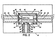
- FIG 2 is a top plan view showing an MMIC chip 38 positioned within a cavity 40 of a conductive packaging fixture 42, according to an embodiment of the present invention. This plan view is also depicted in Figure 3 where the chip 38 has been removed and a dotted rectangular box represents the position of the chip 38. Additionally, Figure 4 shows a side plan view of the chip 38 and the fixture 42 through line 4-4 of Figure 2.
- the chip 38 includes a backside metal layer 44 acting as a ground plane.
- the chip 38 is mounted to the fixture 42 by a conductive epoxy layer 48 attached to the metal layer 44 to provide a ground reference potential connection to the chip 38, and hold the chip 38 at the desirable location within the cavity 40.
- a plurality of ground vias 50 connect backside metal 44 to top of chip, through GaAs substrate, providing reference potential to electrical layout 46.
- substrates 52 are provided to support RF microstrips 54 and substrates 56 are provided to support DC traces 58.
- the substrates 52 and 56 can be made out of any suitablehigh dielectric non-conductive material, such as alumina.
- Each of the substrates 52 and 56 extend into the cavity 40 below the chip 38 to position the microstrips 54 and the traces 58 at the appropriate location below the chip 38, and thus, the substrates 52 and 56 are not on the same plane as the chip 38 as with the embodiment shown in Figure 1. This is represented by the darkened areas around the substrates 52 and 56.
- a raised portion 60 of the fixture 42 is provided below the chip 38 and between the substrates 52 and 54 to allow the chip 38 to be readily mounted to the fixture 42 by the epoxy layer 48 within the design of the present invention.
- a plurality of RF via feedthroughs 62 and DC via feedthroughs 64 are provided that extend through the chip 38, as shown.
- a conductive pad is provided on the top surface of the chip 38 where each via feedthrough 62 and 64 extends through to provide for testing locations and the like on top of the chip 38.
- conductive pads are provided on the bottom surface of the chip 38 using layer 44 to provide a backside electrical connection to the via feedthroughs 62 and 64.
- Microstrip traces 66 are provided on the top surface of the chip 38 to electrically connect the RF feedthrough 62 to the components within the layout section 46.
- the metal layer 44 is appropriately etched away to create open areas 68 in the layer 44. Portions of the metal layer 44 remain as islands 70. Therefore, the entire backside of the chip 38 is not metalized.
- the ground vias 50 at the ends of the chip 38 proximate the microstrips 66 are moved away from the microstrips 66 to be removed from the open areas 68 to make the electrical connection.
- the via feedthroughs 62 extend through the chip 38 and make electrical contact with a solder or epoxy connection 74 that is in electrical contact with the microstrips 54.
- the DC via feedthroughs 64 extend through the chip 38 and make contact with a solder or conductive epoxy contact, that in turn makes electrical contact with the traces 58.
- the chip 38 is maintained right side up, includes pads for electrical access to the desirable testing connection points within the chip 38, and makes a wireless contact to the suitable microstrips 52 and DC traces 56 for connection within the electrical assembly.
- FIG. 5 shows a plan view and Figure 6 shows a cross-sectional view of an MMIC chip layout scheme, according to another embodiment of the invention.
- like components are numbered with the same reference numeral as those reference numerals in Figures 2-4.
- the substrates 52 and 56 are replaced with a single substrate 80 that extends completely through the cavity 40 across the bottom of the chip 38. Because the substrate 80 is not conductive, and the chip 38 would therefore not be electrically connected to the fixture 42 for reference potential purposes, suitable modifications must be made to connect the backside metal layer 44 to the fixture 42.
- an elevated ground plane 82 is provided on the substrate 80 in electrical contact with the conductive epoxy layer 48.
- a plurality of ground vias 84 are provided through the substrate 80 to contact the ground plane 82, thus making the reference potential connection to the backside metal layer 44.
- the packaging scheme of the invention allows the front side of the MMIC chip 38 to be visually inspected for failures and defects even after it is attached to the substrate, and allows the chip 38 to transfer heat to the atmosphere.
- the invention can be accomplished using presently known GaAs processing steps with no additional masking steps because the via hole technology already is utilized on the GaAs wafer, and wafer backside processing is presently performed to produce waferscribe lanes on three inch GaAs wafers.
- FIG. 7 shows a simulation at the bottom level of the chip 38 and top of microstrip substrate to provide inductive tuning to satisfy this purpose.
- a section 90 represents the backside metal 44
- an open area 92 represents the open area 68
- a strip section 94 represents the microstrip 54
- a pad section 96 represents the connection point to the via feedthrough 62 at the bottom of the chip 38.
- a narrower inductive transition section 98 between the strip section 94 and the pad section 96 is provided between the microstrip 54 and the via feedthrough 62 for the tuning purposes.
- Figure 8 shows a simulation at the top level of the chip 38.
- a section 102 represents the top pad and RF via feedthrough 62, a strip section 104 including a widened section 106 is added to the top of the chip 38 to provide a capacitance between the section 104 and the backside metal layer 44 to provide capacitive tuning. Both capacitative and inductive tuning are used in conjunction in this design.
- Figures 9(a) and 9(b) are graphs that show the results of providing this tuning, where frequency is on the horizontal axis and power loss in dB is on the vertical axis.
- Figure 9(a) shows return loss due to RF via structure on graph line 110 and insertion loss on graph line 112 without the tuning elements depicted in Figures 7 and 8.
- Figure 9(b) shows return loss at RF via structure on graph line 114, and insertion loss on graph line 116 with the tuning elements depicted in Figures 7 and 8.
- the tuning elements provide for improved insertion loss and return loss across RF via structure..
- use of specified tuning elements can achieve greater than 19 dB return loss at 50 GHz, and less than .18 dB insertion loss.
Landscapes
- Semiconductor Integrated Circuits (AREA)
- Waveguides (AREA)
- Waveguide Connection Structure (AREA)
Abstract
A wireless MMIC chip packaging scheme where the MMIC chip (38) is
maintained right side up. The MMIC chip (38) is positioned within a cavity (40) of
a fixture (42), where a backside metal layer (44) of the chip (38) is mounted to the
fixture (42) by a conductive epoxy layer (48). RF and DC via feedthroughs (62,
64) are strategically provided through the chip (38), and are electrically connected
to isolated islands (70) in the backside metal layer (44). Substrates (52, 56) are
provided that carry microstrips (54) and electrical traces (56), and that extend
below the chip (38) so that ends of the microstrips (54) and traces (56) make an
electrical connection with the isolated islands (70). In an alternate design, the
substrate (80) extends completely across the backside of the chip (38), and
ground vias (84) extend through the substrate (80) to connect the backside metal
layer (44) to the fixture (42).
Description
- This invention relates generally to wireless packaging for an integrated circuit chip and, more particularly, to wireless packaging for an MMIC chip that includes providing RF and DC via feedthroughs extending into the chip from top circuit layer to backside of the chip to directly connect RF and DC inputs and outputs to microstrips and traces formed on a substrate positioned relative to the backside of the chip.
- Millimeter-wave and/or microwave integrated circuit (MMIC) chips are used in many types of electrical systems that transfer signals at millimeter-wave and microwave frequencies. The millimeter-wave or microwave electrical systems will generally include one or more MMIC chips packaged within a suitable housing. Substrates are positioned within the housing to support microstrips and the like to provide RF connections between the MMIC chips and provide DC power input connections to the chips. The high frequency signals at these wavelengths require specialized RF and DC input and output connections to the chip suitable for state-of-the-art MMIC assembly technology and to minimize losses in a cost effective manner.
- In one MMIC chip packaging design, the RF inputs and outputs and DC power inputs to the MMIC chip employ ribbonbond and wirebond connections to connect the chip to the microstrips on the substrates. Figure 1 shows a top plan view of a
conventional MMIC chip 10 employing these types of electrical connections. The MMICchip 10 is mounted at its backside within acavity 12 of apackaging fixture 14 by a suitable conductive epoxy, solder or the like to position and protect thechip 10. Thefixture 14 can be made of any suitable conductive material, such as an aluminum or brass, and is generally maintained at a reference potential, such as ground. Thechip 10 includes abackside metal layer 16 acting as a ground plane that covers the entire back surface of thechip 10. The epoxy or solder connection between themetal layer 16 and thefixture 14 provides the common reference potential connection to thechip 10. In alternate designs, thebackside metal layer 16 can be at a bias potential, free floating, etc. Anelectrical layout section 18 is formed on GaAs substrate and includes the electrical components associated with theMMIC chip 10 depending on the particular application. In this plan view, the size of thelayer 16 is shown exaggerated relative to thelayout section 18 to better depict the input and output connections to thechip 10 that will be discussed below. - The
chip 10 includes a plurality ofground vias 20 that extend through thechip 10 and are connected to thelayer 16 to allow the electrical components within thesection 18 of thechip 10 to be connected to the common reference potential. A plurality ofDC pads 22 are mounted on top of thechip 10 and are electrically connected toconductive traces 24 that extend into thefixture 14 bywirebonds 26. TheDC pads 22 are appropriately connected to the components in thesection 18 to provide DC voltage potentials to be applied to the components within thechip 10.Microstrips 28 are patterned onnon-conductive substrates 30 positioned within thefixture 14 to transfer the high frequency RF microwave or millimeterwave signals to and from thechip 10. Thesubstrates 30 extend through thefixture 14 into thecavity 12, as shown. Ribbonbonds 32 are electrically connected to themicrostrips 28 and toconductive pads 34 on top of thechip 10. Thepads 34 are electrically connected tomicrostrip lines 36 on thechip 10 to transmit the high frequency RF signals to the electrical components in thesection 18. Theground vias 20 that are provided adjacent to thepads 34 allow for on-wafer measurement capabilities, or for co-planar connection applications, as is well understood in the art. Theribbonbonds 32 generally have a bowed configuration to provide play for thermal and mechanical stresses. In this design, thesubstrates 30 are at the same level as thechip 10 such that themicrostrips 28 are substantially parallel with the top surface of thechip 10, so that thewirebonds 26 and theribbonbonds 32 provide the electrical connections to the top of thechip 10 in an efficient manner. - The connection technique using the
wirebonds 26 and theribbonbonds 32 for the design discussed above, has a number of drawbacks. Particularly, this technique is somewhat labor intensive in that it requires an operator to carefully make the wirebond and ribbonbond connections. Additionally, the ribbonbond connections to the MMICchip 10 degrade the chip performance because theribbonbonds 32 add a finite inductance in series with theMMIC chip 10. This ribbonbond inductance degrades performance, which is most noticeable at microwave and millimeterwave frequencies. It is known in the art that the inductance generated by eachribbonbond 32 can be using an off-chip matching network (not shown) that includes an open circuit stub matching network that negates the inductance of theribbonbonds 32, and produces a low pass filter network that prevents the inductive reactance from degrading circuit performance. However, this method of inductance compensation is time consuming to implement, and requires separate substrate designs depending on the length and the thickness of the connecting ribbon. - Other methods of providing RF inputs and outputs to an MMIC chip are known in the art that do not use ribbonbonds. One method is generally referred to as flip-chip circuit technology, and employs a wireless connection to the MMIC chip. In flip-chip circuit technology, the face (top) of the processed
MMIC chip 10 is soldered or epoxied to a connecting substrate instead of the backside metal layer. Referring to Figure 1, in the flip-chip design, thechip 10 would be flipped over, and various connection points in theelectrical layout section 18 would be electrically connected to solder bumps or the like formed on traces on a mounting substrate to provide the appropriate connections to thechip 10. - Flip-chip circuit technology, however, also has several disadvantages. These disadvantages include trapping heat between the MMIC chip and the mounting substrate because the MMIC chip surface cannot take advantage of heat convection from air circulation. Additionally, the MMIC chip cannot be visually inspected for failure mechanisms after the MMIC chip is mounted on the substrate because the face of the chip is covered by the mounting substrate, and the electrical connections between the MMIC chip and the substrate cannot be checked because the connections are not exposed. Also, the circuit design has to be in coplanar technology. Coplanar technology has notable disadvantages at microwave frequencies: heat dissipation, chip size, and allows only for low level circuit complexity. Further, when the chip is flipped over and mounted to the substrate, the circuit performance changes from when the chip was tested when right side up.
- Thus, there is a need for a wireless MMIC chip interconnection process which allows heat dissipation and troubleshooting of the installed MMIC chip. It is therefore an object of the present invention to provide such a wireless MMIC chip packaging scheme for MMIC microstrip circuits.
- In accordance with the teachings of the present invention, a wireless MMIC chip packaging technique is disclosed where the MMIC chip is mounted right side up. The chip is positioned within a cavity of a fixture, where a backside metal layer of the chip is mounted to the fixture by a conductive epoxy bond or the like. RF and DC via feedthroughs are strategically provided through the chip, and are electrically connected to isolated conductive islands designed in the backside metal layer. Substrates are provided that support microstrips and electrical traces, and that extend into the cavity below the chip so that ends of the microstrips and traces make an electrical connection with the isolated islands. Conductive pads are provided on top of the chip and are connected to the RF and DC via feedthroughs to provide for accessible testing locations. In an alternate design, the substrate extends completely across the backside of the chip, and ground vias are provided through the substrate to connect the backside metal layer to the fixture.
- Additional objects, advantages, and features of the present invention will become apparent from the following description and appended claims, taken in conjunction with the accompanying drawings.
-
- Figure 1 is a top plan view of a conventional MMIC chip packaging layout using wirebond and ribbonbond connections;
- Figure 2 is a top plan view showing a wireless packaging scheme for an MMIC chip, according to an embodiment of the present invention;
- Figure 3 is another top plan view of the wireless packaging scheme for an MMIC chip shown in Figure 2;
- Figure 4 is a side plan view of the packaging scheme shown in Figures 2 and 3;
- Figure 5 is top plan view depicting a wireless packaging scheme for an MMIC chip, according to another embodiment of the present invention;
- Figure 6 is a side plan view of the packaging scheme shown in Figure 5;
- Figure 7 is a simulation depicting inductive tuning elements used in connection with the packaging design of the invention;
- Figure 8 is a simulation depicting capacitive tuning elements used in connection with the packaging design of the invention; and
- Figures 9(a) and 9(b) show electromagnetic simulations depicting the performance of the MMIC chip with and without the tuning elements shown in Figures 7 and 8.
-
- The following description of the preferred embodiments directed to a wireless packaging technique for an MMIC chip is merely exemplary in nature, and is in no way intended to limit the invention or its applications or uses.
- Figure 2 is a top plan view showing an
MMIC chip 38 positioned within acavity 40 of aconductive packaging fixture 42, according to an embodiment of the present invention. This plan view is also depicted in Figure 3 where thechip 38 has been removed and a dotted rectangular box represents the position of thechip 38. Additionally, Figure 4 shows a side plan view of thechip 38 and thefixture 42 through line 4-4 of Figure 2. As with thechip 10 above, thechip 38 includes abackside metal layer 44 acting as a ground plane. Thechip 38 is mounted to thefixture 42 by aconductive epoxy layer 48 attached to themetal layer 44 to provide a ground reference potential connection to thechip 38, and hold thechip 38 at the desirable location within thecavity 40. A plurality of ground vias 50 connectbackside metal 44 to top of chip, through GaAs substrate, providing reference potential toelectrical layout 46. - In this embodiment,
substrates 52 are provided to supportRF microstrips 54 andsubstrates 56 are provided to support DC traces 58. Thesubstrates substrates cavity 40 below thechip 38 to position themicrostrips 54 and thetraces 58 at the appropriate location below thechip 38, and thus, thesubstrates chip 38 as with the embodiment shown in Figure 1. This is represented by the darkened areas around thesubstrates portion 60 of thefixture 42 is provided below thechip 38 and between thesubstrates chip 38 to be readily mounted to thefixture 42 by theepoxy layer 48 within the design of the present invention. - In order to provide a wireless connection to the DC traces 58 and the RF microstrips 54 at the appropriate connection points on the
chip 38, in accordance with the teachings of the present invention, a plurality of RF viafeedthroughs 62 and DC viafeedthroughs 64 are provided that extend through thechip 38, as shown. A conductive pad is provided on the top surface of thechip 38 where each viafeedthrough chip 38. Likewise, conductive pads are provided on the bottom surface of thechip 38 usinglayer 44 to provide a backside electrical connection to the viafeedthroughs chip 38 to electrically connect theRF feedthrough 62 to the components within thelayout section 46. - To electrically isolate the via
feedthroughs metal layer 44, themetal layer 44 is appropriately etched away to createopen areas 68 in thelayer 44. Portions of themetal layer 44 remain asislands 70. Therefore, the entire backside of thechip 38 is not metalized. - The ground vias 50 at the ends of the
chip 38 proximate themicrostrips 66 are moved away from themicrostrips 66 to be removed from theopen areas 68 to make the electrical connection. The viafeedthroughs 62 extend through thechip 38 and make electrical contact with a solder orepoxy connection 74 that is in electrical contact with themicrostrips 54. Likewise, the DC viafeedthroughs 64 extend through thechip 38 and make contact with a solder or conductive epoxy contact, that in turn makes electrical contact with thetraces 58. Thus, thechip 38 is maintained right side up, includes pads for electrical access to the desirable testing connection points within thechip 38, and makes a wireless contact to the suitable microstrips 52 and DC traces 56 for connection within the electrical assembly. - Figure 5 shows a plan view and Figure 6 shows a cross-sectional view of an MMIC chip layout scheme, according to another embodiment of the invention. In these figures, like components are numbered with the same reference numeral as those reference numerals in Figures 2-4. In this embodiment, the
substrates single substrate 80 that extends completely through thecavity 40 across the bottom of thechip 38. Because thesubstrate 80 is not conductive, and thechip 38 would therefore not be electrically connected to thefixture 42 for reference potential purposes, suitable modifications must be made to connect thebackside metal layer 44 to thefixture 42. In this regard, anelevated ground plane 82 is provided on thesubstrate 80 in electrical contact with theconductive epoxy layer 48. To electrically connect theground plane 82 to thefixture 42, a plurality of ground vias 84 are provided through thesubstrate 80 to contact theground plane 82, thus making the reference potential connection to thebackside metal layer 44. - The packaging scheme of the invention allows the front side of the
MMIC chip 38 to be visually inspected for failures and defects even after it is attached to the substrate, and allows thechip 38 to transfer heat to the atmosphere. Moreover, the invention can be accomplished using presently known GaAs processing steps with no additional masking steps because the via hole technology already is utilized on the GaAs wafer, and wafer backside processing is presently performed to produce waferscribe lanes on three inch GaAs wafers. - The use of the RF via
feedthroughs 62 alters the impedance matching between the microstrips 54 and the electrical components of thechip 38. Therefore, tuning elements must be provided to adjust the inductive and capacitive effects of the microstrip and via connections. Figure 7 shows a simulation at the bottom level of thechip 38 and top of microstrip substrate to provide inductive tuning to satisfy this purpose. In this simulation, asection 90 represents thebackside metal 44, anopen area 92 represents theopen area 68, astrip section 94 represents themicrostrip 54, and apad section 96 represents the connection point to the viafeedthrough 62 at the bottom of thechip 38. A narrowerinductive transition section 98 between thestrip section 94 and thepad section 96 is provided between themicrostrip 54 and the viafeedthrough 62 for the tuning purposes. - Figure 8 shows a simulation at the top level of the
chip 38. Asection 102 represents the top pad and RF viafeedthrough 62, astrip section 104 including a widenedsection 106 is added to the top of thechip 38 to provide a capacitance between thesection 104 and thebackside metal layer 44 to provide capacitive tuning. Both capacitative and inductive tuning are used in conjunction in this design. - Figures 9(a) and 9(b) are graphs that show the results of providing this tuning, where frequency is on the horizontal axis and power loss in dB is on the vertical axis. Figure 9(a) shows return loss due to RF via structure on
graph line 110 and insertion loss ongraph line 112 without the tuning elements depicted in Figures 7 and 8. At 50 GHz, there is a return loss of -10.0 dB. Figure 9(b) shows return loss at RF via structure ongraph line 114, and insertion loss ongraph line 116 with the tuning elements depicted in Figures 7 and 8. As is apparent, the tuning elements provide for improved insertion loss and return loss across RF via structure.. In this example, use of specified tuning elements can achieve greater than 19 dB return loss at 50 GHz, and less than .18 dB insertion loss. - The foregoing discussion discloses and describes merely exemplary embodiments of the present invention. One skilled in the art will readily recognize from such discussion, and from the accompanying drawings and claims, that various, changes, modifications and variations can be made therein without departing from the spirit and scope of the invention as defined in the following claims.
Claims (17)
- A packaging assembly for an electrical circuit, said assembly comprising:a packaging housing including a cavity;at least one substrate extending into the cavity, said at least one substrate including at least one microstrip formed on the substrate; andan integrated circuit chip positioned within the cavity relative to the substrate, said integrated circuit chip including a backside metal layer positioned adjacent to the at least one substrate, said integrated circuit chip further including at least one via feed-through extending into the integrated circuit chip and being electrically connected to the at least one microstrip adjacent to the backside metal layer, said via feed-through providing an electrical connection to the chip.
- The assembly according to claim 1 further comprising a conductive epoxy layer, said epoxy layer mounting the integrated circuit chip to the housing, said epoxy layer being connected to the backside metal layer to provide a reference potential connection to the chip.
- The assembly according to claim 1 further comprising an elevated ground plane, said at least one substrate extending completely across the bottom of the chip so that it opposes the metal layer, said ground plane being positioned on the substrate between the substrate and the chip.
- The assembly according to claim 3 further comprising a conductive mounting layer, said conductive layer being connected to the backside metal layer and the elevated ground plane to provide a reference potential connection to the metal layer.
- The assembly according to claim 3 further comprising a plurality of ground vias connected to the housing and extending through the substrate and contacting the ground plane.
- The assembly according to claim 1 further comprising an electrical isolation region formed in the backside metal layer to electrically isolate the at least one via feed-through from the metal layer.
- The assembly according to claim 1 further comprising DC pads attached to a top surface of the chip and electrically connected to the at least one via feed-through.
- The assembly according to claim 1 wherein the at least one substrate extends into the cavity relative to the metal layer and below the integrated circuit chip.
- The assembly according to claim 1 wherein the at least one via feed-through provides an RF electrical connection to the integrated circuit chip.
- The assembly according to claim 1 wherein the at least one via feed-through provides a DC electrical connection to the integrated circuit chip.
- The assembly according to claim 1 further comprising inductive and capacitive tuning elements electrically connected to the at least one via feed-through.
- The assembly according to claim 1 wherein the at least one via feed-through is a plurality of via feed-throughs that provide all of the RF and DC connections to the integrated circuit chip.
- A wireless packaging assembly for an electrical circuit, said assembly comprising:a packaging fixture including a cavity;at least one substrate extending into the cavity, said at least one substrate including a plurality of microstrips formed thereon; andan MMIC chip including a backside metal layer, said chip being mounted within the cavity so that the at least one substrate is below and opposes the backside metal layer, wherein a conductive mounting layer mounts the chip to the fixture and provides a reference potential connection to the chip, said MMIC chip further including a plurality of RF via feed-throughs and DC via feed-throughs extending into the integrated circuit chip and being electrically connected to the plurality of microstrips adjacent to the backside metal layer, said backside metal layer being patterned to provide electrically isolated regions where the via feed-throughs contact the microstrips.
- The assembly according to claim 13 further comprising an elevated ground plane, said substrate extending completely across the bottom of the chip so that it opposes the metal layer, said ground plane being positioned on the substrate between the substrate and the chip.
- The assembly according to claim 13 further comprising a plurality of ground vias connected to the fixture and extending through the substrate and contacting the ground plane.
- The assembly according to claim 13 further comprising inductive and capacitive tuning elements electrically connected to the via feed-throughs.
- A method of providing wireless electrical connections to an integrated circuit, comprising:fabricating the integrated circuit to have a backside metal layer and a plurality of via feed-throughs extending through the integrated circuit;providing a packaging fixture including a cavity;positioning at least one substrate within the fixture that extends into the cavity, said at least one substrate including a plurality of microstrips formed thereon; andmounting the integrated circuit within the cavity so that the plurality of via feed-throughs make electrical contact with the plurality of microstrips adjacent the backside metal layer.
Applications Claiming Priority (2)
| Application Number | Priority Date | Filing Date | Title |
|---|---|---|---|
| US250735 | 1999-02-15 | ||
| US09/250,735 US6118357A (en) | 1999-02-15 | 1999-02-15 | Wireless MMIC chip packaging for microwave and millimeterwave frequencies |
Publications (1)
| Publication Number | Publication Date |
|---|---|
| EP1030368A1 true EP1030368A1 (en) | 2000-08-23 |
Family
ID=22948931
Family Applications (1)
| Application Number | Title | Priority Date | Filing Date |
|---|---|---|---|
| EP00102101A Withdrawn EP1030368A1 (en) | 1999-02-15 | 2000-02-03 | Wireless MMIC chip packaging for microwave and millimeterwave frequencies |
Country Status (3)
| Country | Link |
|---|---|
| US (1) | US6118357A (en) |
| EP (1) | EP1030368A1 (en) |
| JP (1) | JP2000236032A (en) |
Cited By (5)
| Publication number | Priority date | Publication date | Assignee | Title |
|---|---|---|---|---|
| WO2002082537A1 (en) * | 2001-04-06 | 2002-10-17 | Tarja Juhola | High frequency integrated circuit (hfic) microsystems assembly and method for fabricating the same |
| WO2004112134A1 (en) * | 2003-06-12 | 2004-12-23 | Koninklijke Philips Electronics N.V. | Package for a high-frequency electronic device |
| WO2012033641A1 (en) * | 2010-09-10 | 2012-03-15 | Raytheon Company | Monolithic microwave integrated circuit |
| US9318450B1 (en) | 2014-11-24 | 2016-04-19 | Raytheon Company | Patterned conductive epoxy heat-sink attachment in a monolithic microwave integrated circuit (MMIC) |
| DE102008040900B4 (en) | 2007-08-29 | 2023-07-06 | Keysight Technologies, Inc. (n.d.Ges.d.Staates Delaware) | Stacked IC structure and method of forming a stacked IC structure |
Families Citing this family (19)
| Publication number | Priority date | Publication date | Assignee | Title |
|---|---|---|---|---|
| JP4190111B2 (en) * | 1999-10-29 | 2008-12-03 | 富士通株式会社 | High frequency module |
| US6294966B1 (en) | 1999-12-31 | 2001-09-25 | Hei, Inc. | Interconnection device |
| US6612852B1 (en) | 2000-04-13 | 2003-09-02 | Molex Incorporated | Contactless interconnection system |
| US6362972B1 (en) | 2000-04-13 | 2002-03-26 | Molex Incorporated | Contactless interconnection system |
| US6876163B2 (en) * | 2002-10-03 | 2005-04-05 | Visteon Global Technologies, Inc. | DC motor having a braking circuit |
| US7015869B2 (en) * | 2002-11-18 | 2006-03-21 | Visteon Global Technologies, Inc. | High frequency antenna disposed on the surface of a three dimensional substrate |
| US20040104077A1 (en) * | 2002-12-03 | 2004-06-03 | Visteon Global Technologies, Inc. | Minimal differential pressure venting system |
| KR100775414B1 (en) | 2006-01-19 | 2007-11-12 | 센싱테크 주식회사 | Mode Converter in Non-Radiated Microstrip Line Using Metal Jig for Semiconductor Device Attachment |
| KR100870134B1 (en) * | 2007-10-05 | 2008-11-24 | 한국전자통신연구원 | Ultra-Wideband Sealed Surface Mount Package for Ultra-High Frequency Single Integrated Circuits |
| US8390083B2 (en) * | 2009-09-04 | 2013-03-05 | Analog Devices, Inc. | System with recessed sensing or processing elements |
| WO2012051340A1 (en) | 2010-10-12 | 2012-04-19 | Analog Devices, Inc. | Microphone package with embedded asic |
| US8581406B1 (en) * | 2012-04-20 | 2013-11-12 | Raytheon Company | Flip chip mounted monolithic microwave integrated circuit (MMIC) structure |
| CN104576883B (en) | 2013-10-29 | 2018-11-16 | 普因特工程有限公司 | Chip installation array substrate and its manufacturing method |
| US9337522B2 (en) * | 2013-10-30 | 2016-05-10 | Infineon Technologies Ag | Millimeter-wave system including a waveguide transition connected to a transmission line and surrounded by a plurality of vias |
| US9577303B2 (en) * | 2015-01-30 | 2017-02-21 | Raytheon Company | Microwave attenuator module |
| US9520853B2 (en) * | 2015-03-09 | 2016-12-13 | Raytheon Company | Radio frequency (RF) series attenuator module for bridging two RF transmission lines on adjacent circuit substrates |
| US9666558B2 (en) | 2015-06-29 | 2017-05-30 | Point Engineering Co., Ltd. | Substrate for mounting a chip and chip package using the substrate |
| US11088098B2 (en) * | 2019-08-12 | 2021-08-10 | Viasat, Inc. | Integrated structures with antenna elements and IC chips employing edge contact connections |
| CN117733269A (en) * | 2024-02-02 | 2024-03-22 | 北京无线电测量研究所 | Low-void-ratio grounding brazing method for microwave module |
Citations (6)
| Publication number | Priority date | Publication date | Assignee | Title |
|---|---|---|---|---|
| US5158911A (en) * | 1990-08-03 | 1992-10-27 | Thomson Composants Microondes | Method for interconnection between an integrated circuit and a support circuit, and integrated circuit adapted to this method |
| US5406125A (en) * | 1993-04-15 | 1995-04-11 | Martin Marietta Corp. | Semiconductor device having a metalized via hole |
| EP0718905A1 (en) * | 1994-12-21 | 1996-06-26 | Industrial Technology Research Institute | Surface mountable microwave IC package |
| US5635762A (en) * | 1993-05-18 | 1997-06-03 | U.S. Philips Corporation | Flip chip semiconductor device with dual purpose metallized ground conductor |
| DE19832976A1 (en) * | 1997-07-23 | 1999-01-28 | Nec Corp | Reception substrate for HF semiconductor component |
| US5977631A (en) * | 1998-01-06 | 1999-11-02 | Mitsubishi Denki Kabushiki Kaisha | Semiconductor device including a semiconductor package with electromagnetic coupling slots |
Family Cites Families (1)
| Publication number | Priority date | Publication date | Assignee | Title |
|---|---|---|---|---|
| US5049978A (en) * | 1990-09-10 | 1991-09-17 | General Electric Company | Conductively enclosed hybrid integrated circuit assembly using a silicon substrate |
-
1999
- 1999-02-15 US US09/250,735 patent/US6118357A/en not_active Expired - Lifetime
-
2000
- 2000-02-03 EP EP00102101A patent/EP1030368A1/en not_active Withdrawn
- 2000-02-15 JP JP2000036313A patent/JP2000236032A/en active Pending
Patent Citations (6)
| Publication number | Priority date | Publication date | Assignee | Title |
|---|---|---|---|---|
| US5158911A (en) * | 1990-08-03 | 1992-10-27 | Thomson Composants Microondes | Method for interconnection between an integrated circuit and a support circuit, and integrated circuit adapted to this method |
| US5406125A (en) * | 1993-04-15 | 1995-04-11 | Martin Marietta Corp. | Semiconductor device having a metalized via hole |
| US5635762A (en) * | 1993-05-18 | 1997-06-03 | U.S. Philips Corporation | Flip chip semiconductor device with dual purpose metallized ground conductor |
| EP0718905A1 (en) * | 1994-12-21 | 1996-06-26 | Industrial Technology Research Institute | Surface mountable microwave IC package |
| DE19832976A1 (en) * | 1997-07-23 | 1999-01-28 | Nec Corp | Reception substrate for HF semiconductor component |
| US5977631A (en) * | 1998-01-06 | 1999-11-02 | Mitsubishi Denki Kabushiki Kaisha | Semiconductor device including a semiconductor package with electromagnetic coupling slots |
Cited By (6)
| Publication number | Priority date | Publication date | Assignee | Title |
|---|---|---|---|---|
| WO2002082537A1 (en) * | 2001-04-06 | 2002-10-17 | Tarja Juhola | High frequency integrated circuit (hfic) microsystems assembly and method for fabricating the same |
| WO2004112134A1 (en) * | 2003-06-12 | 2004-12-23 | Koninklijke Philips Electronics N.V. | Package for a high-frequency electronic device |
| DE102008040900B4 (en) | 2007-08-29 | 2023-07-06 | Keysight Technologies, Inc. (n.d.Ges.d.Staates Delaware) | Stacked IC structure and method of forming a stacked IC structure |
| WO2012033641A1 (en) * | 2010-09-10 | 2012-03-15 | Raytheon Company | Monolithic microwave integrated circuit |
| US8339790B2 (en) | 2010-09-10 | 2012-12-25 | Raytheon Company | Monolithic microwave integrated circuit |
| US9318450B1 (en) | 2014-11-24 | 2016-04-19 | Raytheon Company | Patterned conductive epoxy heat-sink attachment in a monolithic microwave integrated circuit (MMIC) |
Also Published As
| Publication number | Publication date |
|---|---|
| JP2000236032A (en) | 2000-08-29 |
| US6118357A (en) | 2000-09-12 |
Similar Documents
| Publication | Publication Date | Title |
|---|---|---|
| US6118357A (en) | Wireless MMIC chip packaging for microwave and millimeterwave frequencies | |
| EP0200291B1 (en) | Surface mountable microwave ic package | |
| JP3487639B2 (en) | Semiconductor device | |
| EP0503200B1 (en) | Package for microwave integrated circuit | |
| KR0156334B1 (en) | Semiconductor chip package having shield bonding wire for high frequency and high density | |
| US5583468A (en) | High frequency transition from a microstrip transmission line to an MMIC coplanar waveguide | |
| US5065123A (en) | Waffle wall-configured conducting structure for chip isolation in millimeter wave monolithic subsystem assemblies | |
| US4739448A (en) | Microwave multiport multilayered integrated circuit chip carrier | |
| US5424693A (en) | Surface mountable microwave IC package | |
| EP0595346A1 (en) | Composite microwave module assembly and its connection structure | |
| KR900008206B1 (en) | Semiconductor devices | |
| CN110556365B (en) | Matching circuits for integrated circuit chips | |
| EP3414791B1 (en) | Antenna package for a millimetre wave integrated circuit | |
| US6507110B1 (en) | Microwave device and method for making same | |
| CN111223827B (en) | Transition circuits for integrated circuit chips | |
| EP0117434A1 (en) | Hybrid microwave subsystem | |
| US4992851A (en) | Characteristic impedance-correct chip carrier for microwave semiconductor components | |
| CA1301949C (en) | Device for interconnection and protection of a bare microwave componentchip | |
| US7170361B1 (en) | Method and apparatus of interposing voltage reference traces between signal traces in semiconductor devices | |
| WO1998003999A1 (en) | Rf power package with a dual ground | |
| KR100270954B1 (en) | Wire-bond free input/output interface for gaas ics with means of determining known good die | |
| US4792773A (en) | Ultra high frequency circuit with low parasite capacities | |
| JP4646969B2 (en) | Semiconductor device | |
| CN115693080B (en) | High-power synthesizer implementation method based on thick-film circuit substrate | |
| US6762494B1 (en) | Electronic package substrate with an upper dielectric layer covering high speed signal traces |
Legal Events
| Date | Code | Title | Description |
|---|---|---|---|
| PUAI | Public reference made under article 153(3) epc to a published international application that has entered the european phase |
Free format text: ORIGINAL CODE: 0009012 |
|
| AK | Designated contracting states |
Kind code of ref document: A1 Designated state(s): DE FR GB IT |
|
| AX | Request for extension of the european patent |
Free format text: AL;LT;LV;MK;RO;SI |
|
| 17P | Request for examination filed |
Effective date: 20001006 |
|
| AKX | Designation fees paid |
Free format text: DE FR GB IT |
|
| STAA | Information on the status of an ep patent application or granted ep patent |
Free format text: STATUS: THE APPLICATION HAS BEEN WITHDRAWN |
|
| 18W | Application withdrawn |
Withdrawal date: 20020920 |