EP1030364A2 - Laminated ceramic with multilayer electrodes and method of fabrication - Google Patents
Laminated ceramic with multilayer electrodes and method of fabrication Download PDFInfo
- Publication number
- EP1030364A2 EP1030364A2 EP00301157A EP00301157A EP1030364A2 EP 1030364 A2 EP1030364 A2 EP 1030364A2 EP 00301157 A EP00301157 A EP 00301157A EP 00301157 A EP00301157 A EP 00301157A EP 1030364 A2 EP1030364 A2 EP 1030364A2
- Authority
- EP
- European Patent Office
- Prior art keywords
- layers
- ceramic
- electrodes
- electrically conductive
- conductive material
- Prior art date
- Legal status (The legal status is an assumption and is not a legal conclusion. Google has not performed a legal analysis and makes no representation as to the accuracy of the status listed.)
- Withdrawn
Links
Images



Classifications
-
- H—ELECTRICITY
- H10—SEMICONDUCTOR DEVICES; ELECTRIC SOLID-STATE DEVICES NOT OTHERWISE PROVIDED FOR
- H10W—GENERIC PACKAGES, INTERCONNECTIONS, CONNECTORS OR OTHER CONSTRUCTIONAL DETAILS OF DEVICES COVERED BY CLASS H10
- H10W70/00—Package substrates; Interposers; Redistribution layers [RDL]
- H10W70/01—Manufacture or treatment
- H10W70/05—Manufacture or treatment of insulating or insulated package substrates, or of interposers, or of redistribution layers
- H10W70/095—Manufacture or treatment of insulating or insulated package substrates, or of interposers, or of redistribution layers of vias therein
-
- C—CHEMISTRY; METALLURGY
- C04—CEMENTS; CONCRETE; ARTIFICIAL STONE; CERAMICS; REFRACTORIES
- C04B—LIME, MAGNESIA; SLAG; CEMENTS; COMPOSITIONS THEREOF, e.g. MORTARS, CONCRETE OR LIKE BUILDING MATERIALS; ARTIFICIAL STONE; CERAMICS; REFRACTORIES; TREATMENT OF NATURAL STONE
- C04B37/00—Joining burned ceramic articles with other burned ceramic articles or other articles by heating
- C04B37/02—Joining burned ceramic articles with other burned ceramic articles or other articles by heating with metallic articles
- C04B37/023—Joining burned ceramic articles with other burned ceramic articles or other articles by heating with metallic articles characterised by the interlayer used
- C04B37/026—Joining burned ceramic articles with other burned ceramic articles or other articles by heating with metallic articles characterised by the interlayer used consisting of metals or metal salts
-
- C—CHEMISTRY; METALLURGY
- C23—COATING METALLIC MATERIAL; COATING MATERIAL WITH METALLIC MATERIAL; CHEMICAL SURFACE TREATMENT; DIFFUSION TREATMENT OF METALLIC MATERIAL; COATING BY VACUUM EVAPORATION, BY SPUTTERING, BY ION IMPLANTATION OR BY CHEMICAL VAPOUR DEPOSITION, IN GENERAL; INHIBITING CORROSION OF METALLIC MATERIAL OR INCRUSTATION IN GENERAL
- C23C—COATING METALLIC MATERIAL; COATING MATERIAL WITH METALLIC MATERIAL; SURFACE TREATMENT OF METALLIC MATERIAL BY DIFFUSION INTO THE SURFACE, BY CHEMICAL CONVERSION OR SUBSTITUTION; COATING BY VACUUM EVAPORATION, BY SPUTTERING, BY ION IMPLANTATION OR BY CHEMICAL VAPOUR DEPOSITION, IN GENERAL
- C23C14/00—Coating by vacuum evaporation, by sputtering or by ion implantation of the coating forming material
- C23C14/22—Coating by vacuum evaporation, by sputtering or by ion implantation of the coating forming material characterised by the process of coating
- C23C14/50—Substrate holders
-
- H—ELECTRICITY
- H10—SEMICONDUCTOR DEVICES; ELECTRIC SOLID-STATE DEVICES NOT OTHERWISE PROVIDED FOR
- H10P—GENERIC PROCESSES OR APPARATUS FOR THE MANUFACTURE OR TREATMENT OF DEVICES COVERED BY CLASS H10
- H10P72/00—Handling or holding of wafers, substrates or devices during manufacture or treatment thereof
- H10P72/70—Handling or holding of wafers, substrates or devices during manufacture or treatment thereof for supporting or gripping
- H10P72/72—Handling or holding of wafers, substrates or devices during manufacture or treatment thereof for supporting or gripping using electrostatic chucks
- H10P72/722—Details of electrostatic chucks
-
- H—ELECTRICITY
- H10—SEMICONDUCTOR DEVICES; ELECTRIC SOLID-STATE DEVICES NOT OTHERWISE PROVIDED FOR
- H10W—GENERIC PACKAGES, INTERCONNECTIONS, CONNECTORS OR OTHER CONSTRUCTIONAL DETAILS OF DEVICES COVERED BY CLASS H10
- H10W70/00—Package substrates; Interposers; Redistribution layers [RDL]
- H10W70/01—Manufacture or treatment
- H10W70/05—Manufacture or treatment of insulating or insulated package substrates, or of interposers, or of redistribution layers
-
- H—ELECTRICITY
- H10—SEMICONDUCTOR DEVICES; ELECTRIC SOLID-STATE DEVICES NOT OTHERWISE PROVIDED FOR
- H10W—GENERIC PACKAGES, INTERCONNECTIONS, CONNECTORS OR OTHER CONSTRUCTIONAL DETAILS OF DEVICES COVERED BY CLASS H10
- H10W70/00—Package substrates; Interposers; Redistribution layers [RDL]
- H10W70/60—Insulating or insulated package substrates; Interposers; Redistribution layers
- H10W70/62—Insulating or insulated package substrates; Interposers; Redistribution layers characterised by their interconnections
- H10W70/63—Vias, e.g. via plugs
- H10W70/635—Through-vias
-
- C—CHEMISTRY; METALLURGY
- C04—CEMENTS; CONCRETE; ARTIFICIAL STONE; CERAMICS; REFRACTORIES
- C04B—LIME, MAGNESIA; SLAG; CEMENTS; COMPOSITIONS THEREOF, e.g. MORTARS, CONCRETE OR LIKE BUILDING MATERIALS; ARTIFICIAL STONE; CERAMICS; REFRACTORIES; TREATMENT OF NATURAL STONE
- C04B2237/00—Aspects relating to ceramic laminates or to joining of ceramic articles with other articles by heating
- C04B2237/02—Aspects relating to interlayers, e.g. used to join ceramic articles with other articles by heating
- C04B2237/04—Ceramic interlayers
- C04B2237/08—Non-oxidic interlayers
-
- C—CHEMISTRY; METALLURGY
- C04—CEMENTS; CONCRETE; ARTIFICIAL STONE; CERAMICS; REFRACTORIES
- C04B—LIME, MAGNESIA; SLAG; CEMENTS; COMPOSITIONS THEREOF, e.g. MORTARS, CONCRETE OR LIKE BUILDING MATERIALS; ARTIFICIAL STONE; CERAMICS; REFRACTORIES; TREATMENT OF NATURAL STONE
- C04B2237/00—Aspects relating to ceramic laminates or to joining of ceramic articles with other articles by heating
- C04B2237/02—Aspects relating to interlayers, e.g. used to join ceramic articles with other articles by heating
- C04B2237/12—Metallic interlayers
- C04B2237/122—Metallic interlayers based on refractory metals
-
- C—CHEMISTRY; METALLURGY
- C04—CEMENTS; CONCRETE; ARTIFICIAL STONE; CERAMICS; REFRACTORIES
- C04B—LIME, MAGNESIA; SLAG; CEMENTS; COMPOSITIONS THEREOF, e.g. MORTARS, CONCRETE OR LIKE BUILDING MATERIALS; ARTIFICIAL STONE; CERAMICS; REFRACTORIES; TREATMENT OF NATURAL STONE
- C04B2237/00—Aspects relating to ceramic laminates or to joining of ceramic articles with other articles by heating
- C04B2237/30—Composition of layers of ceramic laminates or of ceramic or metallic articles to be joined by heating, e.g. Si substrates
- C04B2237/32—Ceramic
- C04B2237/36—Non-oxidic
- C04B2237/366—Aluminium nitride
-
- C—CHEMISTRY; METALLURGY
- C04—CEMENTS; CONCRETE; ARTIFICIAL STONE; CERAMICS; REFRACTORIES
- C04B—LIME, MAGNESIA; SLAG; CEMENTS; COMPOSITIONS THEREOF, e.g. MORTARS, CONCRETE OR LIKE BUILDING MATERIALS; ARTIFICIAL STONE; CERAMICS; REFRACTORIES; TREATMENT OF NATURAL STONE
- C04B2237/00—Aspects relating to ceramic laminates or to joining of ceramic articles with other articles by heating
- C04B2237/50—Processing aspects relating to ceramic laminates or to the joining of ceramic articles with other articles by heating
- C04B2237/59—Aspects relating to the structure of the interlayer
- C04B2237/592—Aspects relating to the structure of the interlayer whereby the interlayer is not continuous, e.g. not the whole surface of the smallest substrate is covered by the interlayer
-
- C—CHEMISTRY; METALLURGY
- C04—CEMENTS; CONCRETE; ARTIFICIAL STONE; CERAMICS; REFRACTORIES
- C04B—LIME, MAGNESIA; SLAG; CEMENTS; COMPOSITIONS THEREOF, e.g. MORTARS, CONCRETE OR LIKE BUILDING MATERIALS; ARTIFICIAL STONE; CERAMICS; REFRACTORIES; TREATMENT OF NATURAL STONE
- C04B2237/00—Aspects relating to ceramic laminates or to joining of ceramic articles with other articles by heating
- C04B2237/50—Processing aspects relating to ceramic laminates or to the joining of ceramic articles with other articles by heating
- C04B2237/62—Forming laminates or joined articles comprising holes, channels or other types of openings
-
- H—ELECTRICITY
- H10—SEMICONDUCTOR DEVICES; ELECTRIC SOLID-STATE DEVICES NOT OTHERWISE PROVIDED FOR
- H10W—GENERIC PACKAGES, INTERCONNECTIONS, CONNECTORS OR OTHER CONSTRUCTIONAL DETAILS OF DEVICES COVERED BY CLASS H10
- H10W44/00—Electrical arrangements for controlling or matching impedance
- H10W44/20—Electrical arrangements for controlling or matching impedance at high-frequency [HF] or radio frequency [RF]
- H10W44/203—Electrical connections
- H10W44/209—Vertical interconnections, e.g. vias
- H10W44/212—Coaxial feed-throughs in substrates
Definitions
- the present invention relates to semiconductor wafer processing equipment and, more particularly, to a conductive feedthrough extending from a volume containing atmospheric pressure through a ceramic body into a vacuum chamber, and further relates to a laminated ceramic body with multiple internal electrodes.
- a semiconductor wafer processing system generally contains a vacuum chamber within which is mounted a wafer support pedestal or susceptor.
- the pedestal is used to support the wafer within the chamber during processing.
- the pedestal contains various components which provide heating and/or cooling of the wafer as well as clamping (chucking) of the wafer to retain the wafer in a stationary position upon the pedestal surface.
- clamping is provided by either a mechanical clamp or an electrostatic chuck.
- the space above the pedestal where the wafer is processed is generally maintained at a high vacuum. However, the space below or inside the pedestal is maintained at atmospheric pressure.
- the pedestal may sometime be fabricated of ceramic.
- electrostatic chucks are used to electrostatically attract and retain a semiconductor wafer during processing.
- radiofrequency (RF) power may be coupled to the electrostatic chuck to bias the chuck in order to provide and/or enhance movement of ions in the plasma in the direction of the wafer during processing.
- the electrostatic chuck typically includes a ceramic body in which a pair of electrodes resides and upon application of DC voltage to the electrodes, the chuck electrostatically attracts a semiconductor wafer to the chuck according to the Johnsen-Rahbek effect.
- electrostatic chuck utilizing the Johnsen-Rahbek effect is disclosed in United States Patent 5,656,093 entitled WAFER SPACING MASK FOR A SUBSTRATE SUPPORT CHUCK AND METHOD OF FABRICATING SAME, Burkhart et al. inventors, patented August 12, 1997; this patent is incorporated herein by reference. Further, when the electrostatic chuck is used in high temperature physical vapor deposition of the type noted above, the chuck may be biased by coupling RF power to the chuck. If the electrostatic chuck is RF biased by applying the RE power to electrodes embedded and residing in the semiconductor body, the electrodes and metal feedthroughs to the electrodes must be relatively large and thick to carry the RF power.
- the metal electrodes and metal feedthroughs carrying the RF power have a different coefficient of expansion than the body of ceramic in which they reside and since the metal electrodes and metal feedthroughs are heated during RF biasing, cracking of the body of ceramic can result, causing destruction of the electrostatic chuck, ruination of a partially processed semiconductor wafer residing on the chuck during breakage, and the need to open the chamber and replace the chuck.
- an electrostatic chuck comprising a ceramic body having electrodes residing or embedded therein which do not cause ceramic breakage upon the application of RF bias to the chuck and heating of the electrodes.
- ceramic bodies such as ceramic support pedestals are generally fabricated by stacking a plurality of layers of ceramic material (e.g., aluminum-nitride, alumina, and the like) and then sintering the stack of layers to cure the layers into a unitary, solid ceramic body.
- ceramic material e.g., aluminum-nitride, alumina, and the like
- sintering the stack of layers to cure the layers into a unitary, solid ceramic body.
- a portion of a select number of layers is silk screened with a conductive material (tungsten alloy) prior to the next layer being positioned atop the silk screened layer.
- Each silk screened region is coaxially aligned along a vertical axis through the ceramic body within another conductive region of another layer.
- the stack of silk screened layers are then sintered to form a solid ceramic body containing a plurality of stacked conductive electrodes.
- Conductive vias are then formed vertically into one surface of the ceramic body to intersect the embedded electrodes. These vias are formed by drilling, bead blasting, etching, or some other process used to generate bores in the ceramic body. Using a physical vapor deposition (PVD), chemical vapor deposition (CVD), brazing or other means of metal deposition, the vias are filled with a conductive material such that the embedded electrodes are interconnected by one or more vertical conductive vias. Depending on the specific procedure used for this via-filling step, the surface may or may not be masked. Suffice to say that the exact procedure employed is not critical to practicing the present invention. A top end of the vias are exposed by lapping the surface of the ceramic body. As such, electrodes and other conductors can be sputtered onto the surface of the ceramic body and connect to the exposed ends of the vias.
- PVD physical vapor deposition
- CVD chemical vapor deposition
- brazing or other means of metal deposition the vias are filled with a
- conductive vias may also be formed by vertically boring through the layers, prior to sintering (i.e., while the ceramic is in a green state), and filling the vias with a conductive paste containing titanium (Ti), titanium nitride (TiN) or tungsten (W).
- These vias may be formed by inserting a solid cylindrical probe into the stack of green state ceramic, then packing the conductive paste into the bore. Subsequent sintering will allow both the ceramic layers and paste to harden, with the electrodes being interconnected by vertical conductive vias.
- a bore is formed into the surface of the ceramic body passing through (intersecting) one or more of the layers of electrodes.
- An electrical connector member, or pin is then brazed into this bore such that the pin conductively connects to the intersected layers of electrode.
- a conductive path is formed between the conductive vias on one side of the ceramic body (e.g., the vacuum side) and the electrical connector on the other side of the ceramic body (e.g., the atmosphere side).
- This feedthrough is completely vacuum-sealed and permits a variety of electrical connections to be made to the feedthrough on the vacuum side of the ceramic body.
- two or more conductive electrode stacks can be fashioned in various, laterally disparate, locations in the ceramic body. These electrode stacks are laterally interconnected with one another through conductive traces deposited (silk screened) between the ceramic layers.
- the inventive feedthrough is used in a PVD system where the ceramic body is a Johnsen-Rahbek electrostatic chuck, and the feedthrough connector of the present invention provides current to a surface electrode located on the vacuum side of the chuck.
- a laminated ceramic body having multiple spaced-apart electrodes formed therein, and an electrical connecting pin for the electrodes, is provided which permits the application of RF power with increased current capacity without the above-noted ceramic breakage due to electrode heating upon the application of the RF power.
- This structure is particularly useful as an RF biasable electrostatic chuck for semiconductor wafer processing such as high temperature physical vapor deposition.
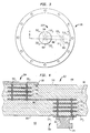
- FIG. 1 depicts a top plan view of an illustrative ceramic body containing the feedthrough of the present invention.
- the ceramic body is a ceramic wafer support pedestal, e.g., a Johnsen-Rahbek electrostatic chuck, for a semiconductor wafer processing system such as a physical vapor deposition system.
- a ceramic wafer support pedestal e.g., a Johnsen-Rahbek electrostatic chuck
- a semiconductor wafer processing system such as a physical vapor deposition system.
- inventive feedthrough finds use in any application of a ceramic body where a conductive feedthrough is necessary.
- Pedestal 100 contains a circumferential mounting flange 102 having a plurality of mounting bores 106.
- the support surface 104 of the pedestal 100 has illustratively affixed thereto an electrode 108.
- an electrode 108 Although a single, centrally-located electrode is shown to illustrate one application of the invention, a multitude of electrodes may be affixed to the surface, or no electrode at all may be used and a feedthrough 110 may be positioned to supply electrical current to diagnostic equipment within a vacuum chamber.
- the feedthrough 110 of the present invention connects the vacuum side of the pedestal, e.g., the side that supports the wafer, to the atmosphere side of the pedestal.
- FIG. 2 depicts a cross-sectional view of a portion of the pedestal 100 taken along 2-2 of FIG. 1.
- This first embodiment of the invention is a single, vertical feedthrough 110 that conductively connects the vacuum side 50 of the pedestal 100 to the atmosphere side 52 of the pedestal 100.
- this feedthrough is supplying power to a conductive electrode positioned on the vacuum side of the pedestal, i.e., the electrode 108 affixed to surface 104.
- the atmosphere side 52 of the pedestal is located below surface 202 of the pedestal 100.
- the feedthrough 110 contains a plurality of conductive layers 206 (e.g., 206 1 , 206 2 , 206 3 , 206 4 , and 206 5 ) arranged vertically within the ceramic body and interconnected by a plurality of vias 208 (e.g., 208 1 , 208 2 , 208 3 and 208 4 ).
- the atmosphere side 52 is connected to the electrodes 206 by a bore 210 and a conductive pin 214 that is braised into the bore such that the pin electrically connects to one or more of the electrode layers 206.
- the ceramic body represented by the pedestal 100, is fabricated of a plurality of stacked layers of ceramic material 204 1 , 204 2 , 204 3 ... 204 8 .
- the layers of ceramic material are "dough-like" and are easily cut and shaped into a desired form. This state is commonly referred to as the "green state”.
- the electrodes 206 are silk screened upon selected layers. The silk screened regions are formed in a vertical stack as each of the ceramic layers are positioned. The silk screened regions are generally coaxially aligned along a vertical axis through the stack of ceramic layers.
- the electrodes are fabricated of a tungsten alloy that, when sintered, solidifies into a tungsten electrode.
- the stack is dewaxed to bake out any hydrocarbons in the ceramic material. Then, the stack is cured by sintering the ceramic layers at approximately 2000 deg. C. within a nitrogen atmosphere.
- one or more conductive vias are vertically formed into the vacuum side 50 of the ceramic body 100.
- These vias 208 are generally created by boring a hole in the ceramic body such that the hole passes through the plurality of ceramic layers 204 and through a plurality of electrodes 206. These bores are formed in the ceramic using conventional boring techniques such as bead blasting, drilling, etching and the like.
- the vias are completed by depositing a conductive material (e.g., a tungsten alloy) into the holes to interconnect the electrodes 206.
- Such deposition is accomplished using conventional techniques such as physical vapor deposition (PVD), chemical vapor deposition (CVD), or other means of depositing metals.
- PVD physical vapor deposition
- CVD chemical vapor deposition
- the surface 104 of the ceramic body 100 is lapped to expose the top end of the vias. Once exposed, a conductive layer 108 can be sputtered on the surface 104. The exposed vias bond with the conductive layer 108. Alternatively, wires, current probes, and other electrical circuitry can be connected to the exposed vias.
- these conductive vias may be formed by boring through the ceramic layers in their pre-cured, green state (prior to sintering), and then filling the bores with a conductive paste containing metals such as titanium, titanium nitride or tungsten. Subsequent sintering will allow the ceramic layers and paste to harden, with the electrodes being interconnected by vertical conductive vias.
- the bores may be formed in each layer and the layers aligned to produce a contiguous bore through the stack of layers, or a bore may be formed by pushing a cylindrical probe through the stacked layers. In either instance, once the bore is formed in the stack, the conductive paste is packed into the bore. Then, the assembly is sintered.
- a bore 210 is formed into the surface 202 on the atmosphere side 52 of the ceramic body 100.
- a shaft 216 of a conductive pin 218 is then brazed into the bore 210 such that the pin is in conductive contact with one or more of the electrodes 206.
- the conductive via 208 is electrically connected to the pin 218 and provides a conductive path through the ceramic body.
- the vias 208 are then be connected to, for example, an electrode 108 that is affixed to the surface 104 of the pedestal 100. As such, electric power can be applied to the atmosphere side of the ceramic body, and the power is carried through the feedthrough to the electrode 108.
- the first illustrative embodiment of the invention depicts a pin connector on the atmosphere side of the ceramic body and the via connector on the vacuum side of the ceramic body, obviously the pin connector could be used on the vacuum side and the via connector used on the atmosphere side.
- a feedthrough may also be constructed having pin connectors on both sides of the ceramic body or a via connector on both sides of the ceramic body.
- FIG. 3 depicts a top plan view of an alternative embodiment of the present invention.
- This embodiment contains a ceramic body 300 (e.g., a ceramic wafer support pedestal) with a feedthrough 302 electrically connecting a vacuum side 400 to an atmosphere side 402 of the ceramic body 300.
- this embodiment of the invention has the location of the pin connector 306 laterally offset from the location of the via connector 304.
- a centrally located electrode 108 affixed to the support surface of the pedestal 100 is connected through an offset feedthrough 302 to the atmosphere side 402 of the pedestal.
- FIG. 4 depicts a cross-sectional view of the alternative embodiment taken along line 4-4 of FIG. 3.
- the offset feedthrough 302 contains a pair of partial feedthroughs 304 and 306. These partial feedthroughs are laterally distant from one another and interconnected by a bus electrode 308.
- a plurality of coaxially aligned electrode layers 316 1 , 316 2 , 316 3 are formed within the ceramic body 300.
- a plurality of coaxially aligned electrodes 310 1 , 310 2 , and 310 3 are formed in the ceramic body 300.
- the electrodes 316 are laterally displaced from the electrodes 310.
- the two sets of electrodes are interconnected by bus 308.
- the bus is formed by silk screening a conductive trace upon one of the ceramic layers that forms the ceramic body such that one end of the trace forms an electrode in one set of electrodes and the other end of the trace forms an electrode in the other set of electrodes.
- the bus 308 interconnects the two sets of electrodes 316 and 310.
- a plurality of conductive vias 312 1 , 312 2 , 312 3 and 312 4 are formed vertically into the ceramic body to interconnect the electrodes 310.
- the electrodes 316 are interconnected by vias 314 1 , 314 2 , 314 3 and 314 4 .
- the surfaces 318 and 320 of the ceramic body 100 are lapped to remove any residual conductive materials and to expose the vias 314 and 312.
- these conductive vias may be formed by boring through the ceramic layers in their pre-cured, green state (prior to sintering), and then filling the bores with a conductive paste containing a metal such as Ti, TiN or W. Subsequent sintering will allow the ceramic layers and paste to harden, with the electrodes being interconnected by vertical conductive vias.
- electrodes 108 and 322 are deposited upon the surfaces of the ceramic body 100 using conventional metalization techniques. Then, an electrical contact pin 324 is brazed or soldered to the conductive pad 322. As such, when electrical current is applied to pin 324, that current flows to the electrode 108 through the offset feedthrough 302.
- a conductive pin 214 of FIG. 2 could be substituted for the surface mounted pin 324.
- a pin, surface mount or not, could be used on the vacuum side of the ceramic body.
- FIG. 5a is a partial transverse vertical cross-sectional view of an illustrative laminated ceramic body containing multilayer electrodes in accordance with the present invention.
- the ceramic body may be, for example, a ceramic wafer support pedestal, i.e., a Johnsen-Rahbek electrostatic chuck for a semiconductor wafer processing system such as a physical vapor deposition system.
- a ceramic wafer support pedestal i.e., a Johnsen-Rahbek electrostatic chuck for a semiconductor wafer processing system such as a physical vapor deposition system.
- this invention can find use in any application requiring a ceramic body and an internal electrode.
- FIG. 5a depicts apparatus 502 includes a body 504 of ceramic, an electrode 506 embedded in the body of ceramic and an electrical connector 508 or connecting pin.
- the body 504 of ceramic may be fabricated of a plurality of stacked layers of ceramic material 504 1 , 504 2 ... 504 7 in the same manner and of the same ceramic material that the stacked layers of ceramic material 204 1 , 204 2 ... 204 8 are fabricated as described hereinabove to form the pedestal 100 shown in FIGS. 1 and 2.
- the electrode 506 includes a plurality of axially aligned (aligned along the axis 509 in FIG. 5a), parallel spaced-apart electrodes 506 1 , 506 2 ... 506 4 and may be fabricated in the same manner and of the same electrically conductive material that the plurality of electrodes or conductive layers 206 1 , 206 2 ... 206 5 are fabricated as described hereinabove to form the plurality of conductive layers or electrodes 206 1 , 206 2 ... 206 5 shown in FIG. 2. In this manner, the electrode 506 is "distributed" such that each layer will handle a portion of the RF current. As such, the RF current is carried by a large cumulative surface area of the layers 506 1 , 506 2 ... 506 5 .
- a bore 512 is suitably formed extending partially into the body of ceramic 504 and the forward end of the electrical connector member or pin 508 is inserted into the bore to intersect and to be mechanically and electrically connected to, such as by brazing or soldering, the electrodes 506 3 and 506 4 .
- the pin 508 needs only contact a subset of all the layers, e.g., two of seven, or even just one, because the RF energy supplied to directly connected electrodes will capacitively couple to the remaining (floating) electrode layers.
- Apparatus 502 is particularly useful as a ceramic pedestal for supporting a semiconductor wafer during processing and is particularly useful for coupling RF power to the electrode 506 and electrical connector 508 as may be required for wafer processing in high temperature physical vapor deposition. It will be understood that this is to provide RF on or beneath the wafer to attract ions from the plasma towards the substrate. Since the electrode 506 is comprised of a plurality of relatively thin electrodes 506 1 , 506 2 ... 506 4 , less heating, and/or less concentration of thermal stress in localized portions of the chuck, is produced on coupling of RF power to the electrical connector 508 and electrode 506.
- the apparatus 502 will include the mounting flange 102 provided with mounting bores 106 (or other mounting hardware) shown in FIG. 1.
- apparatus 502 may include two sets of electrodes 506a and 506b, and electrical connecting pins 508a and 508b, spaced laterally from each other, as shown in FIG. 5b.
- Two conductive vias 514a and 514b are used to directly connect the bottom layer electrodes (506a 4 , 506b 4 ) to the top layer electrodes (506a 1 , 506b 1 ) within each set of electrodes, 506a and 506b.
- the intermediate layer electrodes (506a 2 , 506a 3 , 506b 2 , 506b 3 ) are illustrated as "broken" around the vias 514a and 514b to emphasize that there is no direct connection between these electrodes (506a 2 , 506a 3 , 506b 2 and 506b 3 ) and the conductive vias 514a and 514b.
- the apparatus 502 is particularly useful as a RF biased electrostatic chuck for both electrostatically retaining a semiconductor wafer and biasing the wafer. Both RF and DC voltages are supplied to the two electrical connecting pins 508a and 508b.
- the DC voltage applied to the two pins (508a, 508b) and to the top electrodes (506a 1 , 506b 1 ) is used to attract a semiconductor wafer to the apparatus 502 in accordance with the Johnsen Rahbek effect.
- the RF power applied or coupled to the pair of connecting pins (508a, 508b) provides the RF bias necessary for wafer processing.
- pins 508a and 508b are electrically connected to the two bottom electrodes 506a 4 and 506b 4 .
- the RF power from the bottom electrodes 506a 4 and 506b 4 is coupled to the top of the chuck by a direct connection to the top electrodes (506a 1 , 506b 1 ) through the two conductive vias (514a, 514b), and capacitive coupling via the other floating electrodes (506a 2 , 506b 2 , 506a 3 , 506b 3 ).
- This RF bias is then coupled to the entire wafer through the top electrodes 506a 1 and 506b 1 .
- such distributed RF coupling through multiple-layered electrodes can minimize local thermal stress that may otherwise arise from excessive heating when only a single electrode is used. It is understood that the embodiment shown in Fig.
- this embodiment may be fabricated using different combinations of the same process steps (stacking material layers, drilling and filling conductive vias and sintering) previously described.
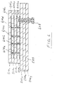
- FIG. 6 Another alternative embodiment is shown in FIG. 6, where a pin 608 is shown to intersect a bottom layer electrode 606 4 within the chuck body 504. Multiple direct connections are formed between this bottom electrode 606 4 and the top electrode 606 1 , as illustrated by the conductive vias 614a, 614b, 614c, and 614d. Again, intermediate electrodes 606 3 and 606 2 are shown as "broken" around these conductive vias 614a, 614b, 614c, and 614d to emphasize that there is no direct connection between these electrodes (606 3 and 606 2 ) and the conductive vias (614a, 614b, 614c, and 614d). Similar to the embodiment in FIG. 5b, both RF and DC powers may be supplied to the pin 608.
- capacitive coupling of RF power takes place via the intermediate electrodes 606 3 and 606 2 .
- the DC and RF powers are both coupled to the top electrode 606 1 through multiple direct connections provided by the vias 614a, 614b, 614c and 614d. Again, such a configuration minimizes the potential of breakage of the chuck due to local thermal stress that may otherwise arise if the power were concentrated on a single connection alone.
Landscapes
- Chemical & Material Sciences (AREA)
- Engineering & Computer Science (AREA)
- Organic Chemistry (AREA)
- Materials Engineering (AREA)
- Ceramic Engineering (AREA)
- Mechanical Engineering (AREA)
- Metallurgy (AREA)
- Chemical Kinetics & Catalysis (AREA)
- Structural Engineering (AREA)
- Container, Conveyance, Adherence, Positioning, Of Wafer (AREA)
- Connections Arranged To Contact A Plurality Of Conductors (AREA)
- Physical Deposition Of Substances That Are Components Of Semiconductor Devices (AREA)
- Manufacturing Of Electrical Connectors (AREA)
- Laminated Bodies (AREA)
- Ceramic Capacitors (AREA)
Abstract
Description
Claims (23)
- Apparatus including ceramic body and electrode, comprising:a body of ceramic and an electrode including a plurality of parallel spaced-apart electrodes embedded in said ceramic body; andan electrical connector extending partially inwardly into said ceramic body, intersecting and being connected mechanically and electrically to at least one electrode of said plurality of parallel spaced-apart electrodes.
- The apparatus according to Claim 1 wherein said ceramic body comprises a plurality of sintered layers of ceramic.
- The apparatus according to Claim 2 wherein said sintered ceramic is sintered aluminum nitride.
- The apparatus according to Claim 1 wherein said electrodes comprise a plurality of parallel spaced-apart layers of solidified electrically conductive material.
- The apparatus according to Claim 4 wherein said solidified electrically conductive material is solidified tungsten alloy.
- The apparatus according to Claim 1 wherein said electrical connector intersects and is mechanically and electrically interconnected to at least two of said electrodes of said plurality of electrodes.
- The apparatus according to Claim 1 wherein said plurality of parallel spaced-apart electrodes includes a first plurality and a second plurality, wherein said electrical connector extends partially into said body of ceramic and intersects and mechanically and electrically interconnects with said first plurality of electrodes and wherein said electrical connector is capacitively electrically coupled to said second plurality of electrodes by portions of said sintered ceramic layers residing intermediate said second plurality of electrodes.
- The apparatus according to Claim 1 wherein a top most electrode within said plurality of parallel spaced-apart electrodes is directly connected to at least one of said electrodes being intersected by and connected to said electrical connector.
- The apparatus according to Claim 1, wherein said one electrode being intersected by and connected to said electrical connector is a bottom most electrode within said plurality of parallel spaced-apart electrodes, and said bottom-most electrode is directly connected to a top-most electrode within said plurality of parallel spaced-apart electrodes.
- Method of fabricating a body of ceramic and electrodes, comprising:providing a plurality of layers of ceramic material;depositing a plurality of aligned, parallel spaced-apart layers of electrically conductive material on selected ones of said plurality of layers of ceramic material;sintering said plurality of layers of ceramic material to form the ceramic body and forming a plurality of parallel spaced-apart electrodes from said layers of deposited electrically conductive material by solidifying said layers of deposited electrically conductive material during said sintering;forming a bore extending partially and perpendicularly into said body of ceramic;inserting an electrically conductive member into said bore; andmechanically and electrically interconnecting said electrical connecting member with at least one of said solidified layers of deposited material.
- The method according to Claim 10 wherein said depositing step is the step of silk screening a plurality of aligned, parallel spaced-apart layers of electrically conductive material on selected ones of said plurality of layers of ceramic material.
- The method according to Claim 10 wherein said depositing step is the step of silk screening a plurality of aligned, parallel spaced-apart layers of conductive paste containing a metal such as titanium, titanium nitride, or tungsten on selected ones of said plurality of layers of ceramic material.
- The method according to Claim 10 wherein said sintering step is the step of sintering a plurality of layers of aluminum nitride at approximately 2,000 deg. C. within a nitrogen atmosphere to form the ceramic body.
- The method according to Claim 10 wherein said step of mechanically and electrically interconnecting said electrical connecting member with at least one of said solidified layers of deposited material is the step of soldering said electrical connecting member to at least one of said solidified layers of deposited material.
- The method according to Claim 10 wherein said step of mechanically and electrically interconnecting said electrical connecting member with at least one of said solidified layers of deposited material is the step of brazing said electrical connecting member to at least one of said solidified layers of deposited material.
- Method of fabricating a body of ceramic and electrodes, comprising:providing a plurality of ceramic material layers;depositing a plurality of aligned, parallel spaced-apart layers of electrically conductive material on selected ones of said plurality of ceramic material layers;forming at least one bore extending perpendicularly through at least one of said plurality of ceramic material layers and intersecting at least one of said plurality of layers of electrically conductive material;filling said bore with an electrically conductive paste;sintering said plurality of ceramic material layers to form the ceramic body and forming a plurality of parallel spaced-apart electrodes from said layers of deposited electrically conductive material by solidifying said layers of deposited electrically conductive material during said sintering so as to mechanically and electrically interconnect said electrically conductive paste with at least one of said solidified layers of deposited electrically conductive material.
- The method according to Claim 16 wherein said depositing step is the step of silk screening a plurality of aligned, parallel spaced-apart layers of electrically conductive material on selected ones of said plurality of layers of ceramic material.
- The method according to Claim 16 wherein said conductive paste contains a metal such as titanium, titanium nitride or tungsten.
- The method according to Claim 16 wherein said sintering step is the step of sintering a plurality of layers of aluminum nitride at approximately 2,000 deg. C. within a nitrogen atmosphere to form the ceramic body.
- Method of fabricating a body of ceramic and electrodes, comprising:providing a plurality of ceramic material layers and a plurality of electrically conductive material layers;forming bores through at least one of said plurality of ceramic material layers and at least one of said electrically conductive material layers;aligning said bores of said plurality of ceramic material layers with said bores of said plurality of electrically conductive material layers;depositing said plurality of aligned, parallel spaced-apart layers of electrically conductive material on selected ones of said plurality of ceramic material layers;filling said bore with an electrically conductive paste;sintering said plurality of ceramic material layers to form the ceramic body and forming a plurality of parallel spaced-apart electrodes from said layers of deposited electrically conductive material by solidifying said layers of deposited electrically conductive material during said sintering so as to mechanically and electrically interconnect said electrically conductive paste with at least one of said solidified layers of deposited electrically conductive material.
- The method according to Claim 20 wherein said depositing step is the step of silk screening a plurality of aligned, parallel spaced-apart layers of electrically conductive material on selected ones of said plurality of layers of ceramic material.
- The method according to Claim 20 wherein said electrically conductive paste contains a metal such as titanium, titanium nitride, or tungsten.
- The method according to Claim 20 wherein said sintering step is the step of sintering a plurality of layers of aluminum nitride at approximately 2,000 deg. C. within a nitrogen atmosphere to form the ceramic body.
Applications Claiming Priority (2)
| Application Number | Priority Date | Filing Date | Title |
|---|---|---|---|
| US251697 | 1999-02-17 | ||
| US09/251,697 US6303879B1 (en) | 1997-04-01 | 1999-02-17 | Laminated ceramic with multilayer electrodes and method of fabrication |
Publications (2)
| Publication Number | Publication Date |
|---|---|
| EP1030364A2 true EP1030364A2 (en) | 2000-08-23 |
| EP1030364A3 EP1030364A3 (en) | 2003-09-03 |
Family
ID=22953036
Family Applications (1)
| Application Number | Title | Priority Date | Filing Date |
|---|---|---|---|
| EP00301157A Withdrawn EP1030364A3 (en) | 1999-02-17 | 2000-02-15 | Laminated ceramic with multilayer electrodes and method of fabrication |
Country Status (4)
| Country | Link |
|---|---|
| US (1) | US6303879B1 (en) |
| EP (1) | EP1030364A3 (en) |
| JP (2) | JP5004376B2 (en) |
| KR (1) | KR100682172B1 (en) |
Cited By (7)
| Publication number | Priority date | Publication date | Assignee | Title |
|---|---|---|---|---|
| WO2001043183A3 (en) * | 1999-12-09 | 2002-05-10 | Saint Gobain Ceramics | Electrostatic chuck, susceptor and method for fabrication |
| US6723274B1 (en) | 1999-12-09 | 2004-04-20 | Saint-Gobain Ceramics & Plastics, Inc. | High-purity low-resistivity electrostatic chucks |
| US6744618B2 (en) | 1999-12-09 | 2004-06-01 | Saint-Gobain Ceramics & Plastics, Inc. | Electrostatic chucks with flat film electrode |
| DE102004041049A1 (en) * | 2004-07-02 | 2006-01-26 | VenTec Gesellschaft für Venturekapital und Unternehmensberatung mbH | Mobile, electrostatic substrate click for wafers in semiconductor manufacture, comprises additional capacitor structures for charge storage, extending over several electrode levels, on support substrate |
| CN103050859A (en) * | 2011-10-14 | 2013-04-17 | 利宝嘉电业(深圳)有限公司 | Automatic production process and automatic production device of audio signal plug |
| EP3642870A4 (en) * | 2017-06-22 | 2021-04-07 | Applied Materials, Inc. | ELECTROSTATIC SUPPORT FOR CHIP FIXING APPLICATIONS |
| US20220310434A1 (en) * | 2021-03-24 | 2022-09-29 | Shinko Electric Industries Co., Ltd. | Electrostatic chuck and substrate fixing device |
Families Citing this family (30)
| Publication number | Priority date | Publication date | Assignee | Title |
|---|---|---|---|---|
| US6189209B1 (en) * | 1998-10-27 | 2001-02-20 | Texas Instruments Incorporated | Method for reducing via resistance in small high aspect ratio holes filled using aluminum extrusion |
| WO2001035459A1 (en) | 1999-11-10 | 2001-05-17 | Ibiden Co., Ltd. | Ceramic substrate |
| US6593535B2 (en) * | 2001-06-26 | 2003-07-15 | Teradyne, Inc. | Direct inner layer interconnect for a high speed printed circuit board |
| DE10205450A1 (en) * | 2002-02-08 | 2003-08-28 | Infineon Technologies Ag | Circuit carrier and manufacture of the same |
| KR100497953B1 (en) * | 2002-08-05 | 2005-06-29 | 한국화학연구원 | conductive ceramic electrode and including a electrostatic chuck |
| US20060118332A1 (en) * | 2004-12-02 | 2006-06-08 | Litton Systems, Inc. | Multilayered circuit board for high-speed, differential signals |
| JP5072289B2 (en) * | 2006-08-30 | 2012-11-14 | 京セラ株式会社 | Airtight terminal |
| JP2008108703A (en) * | 2006-09-28 | 2008-05-08 | Covalent Materials Corp | Planar heater and semiconductor heat treatment apparatus provided with the heater |
| JP2008153543A (en) * | 2006-12-19 | 2008-07-03 | Shinko Electric Ind Co Ltd | Electrostatic chuck |
| KR101398634B1 (en) * | 2008-07-11 | 2014-05-22 | 삼성전자주식회사 | Interconnection structure and electronic device employing the same |
| KR100907864B1 (en) * | 2008-09-30 | 2009-07-14 | 주식회사 아이엠텍 | Space transformer for probe card having isolation resistor and manufacturing method thereof |
| US8378495B2 (en) * | 2009-08-10 | 2013-02-19 | Texas Instruments Incorporated | Integrated circuit (IC) having TSVS with dielectric crack suppression structures |
| JP2011082450A (en) * | 2009-10-09 | 2011-04-21 | Elpida Memory Inc | Semiconductor device, and information processing system with the same |
| JP5348439B2 (en) * | 2011-09-30 | 2013-11-20 | Toto株式会社 | Electrostatic chuck |
| JP6196612B2 (en) | 2012-03-07 | 2017-09-13 | 日本特殊陶業株式会社 | Conveying device and ceramic member |
| US9518326B2 (en) | 2013-10-21 | 2016-12-13 | Applied Materials, Inc. | Method for forming an electrostatic chuck using film printing technology |
| US9101038B2 (en) | 2013-12-20 | 2015-08-04 | Lam Research Corporation | Electrostatic chuck including declamping electrode and method of declamping |
| US9374910B2 (en) * | 2013-12-31 | 2016-06-21 | International Business Machines Corporation | Printed circuit board copper plane repair |
| KR101541051B1 (en) * | 2014-03-24 | 2015-07-31 | (주)보부하이테크 | Manufacturing method of Electrostatic Chuck with Multi-Layer Electrode Structure and Electrostatic Chuck with Multi-Layer Electrode Structure manufactured by the same |
| US10002782B2 (en) | 2014-10-17 | 2018-06-19 | Lam Research Corporation | ESC assembly including an electrically conductive gasket for uniform RF power delivery therethrough |
| US9673025B2 (en) * | 2015-07-27 | 2017-06-06 | Lam Research Corporation | Electrostatic chuck including embedded faraday cage for RF delivery and associated methods for operation, monitoring, and control |
| KR102513443B1 (en) * | 2016-03-15 | 2023-03-24 | 삼성전자주식회사 | electrostatic chuck and substrate processing apparatus including the same |
| TWI641078B (en) * | 2016-05-31 | 2018-11-11 | 日商日本特殊陶業股份有限公司 | Laminated heating element |
| US10892179B2 (en) * | 2016-11-08 | 2021-01-12 | Lam Research Corporation | Electrostatic chuck including clamp electrode assembly forming portion of Faraday cage for RF delivery and associated methods |
| US11289355B2 (en) * | 2017-06-02 | 2022-03-29 | Lam Research Corporation | Electrostatic chuck for use in semiconductor processing |
| JPWO2020195636A1 (en) * | 2019-03-22 | 2020-10-01 | ||
| US12238827B2 (en) * | 2019-03-28 | 2025-02-25 | Kyocera Corporation | Base structure and wafer placing device |
| US12183601B2 (en) * | 2019-10-18 | 2024-12-31 | Kyocera Corporation | Structural body and heating apparatus |
| JP7550685B2 (en) * | 2021-03-17 | 2024-09-13 | 新光電気工業株式会社 | Electrostatic chuck and substrate fixing device |
| WO2022255118A1 (en) * | 2021-06-01 | 2022-12-08 | 東京エレクトロン株式会社 | Plasma processing device and substrate supporter |
Family Cites Families (27)
| Publication number | Priority date | Publication date | Assignee | Title |
|---|---|---|---|---|
| US3346689A (en) | 1965-01-29 | 1967-10-10 | Philco Ford Corp | Multilayer circuit board suing epoxy cards and silver epoxy connectors |
| US4095866A (en) | 1977-05-19 | 1978-06-20 | Ncr Corporation | High density printed circuit board and edge connector assembly |
| US4456786A (en) * | 1979-11-19 | 1984-06-26 | James C. Kyle | Terminal assembly for heart pacemaker |
| FR2567684B1 (en) | 1984-07-10 | 1988-11-04 | Nec Corp | MODULE HAVING A MULTILAYER CERAMIC SUBSTRATE AND A MULTILAYER CIRCUIT ON THE SUBSTRATE AND METHOD FOR THE PRODUCTION THEREOF |
| JPH0760849B2 (en) | 1986-06-05 | 1995-06-28 | 東陶機器株式会社 | Electrostatic chuck plate |
| JPS63193844U (en) * | 1987-05-30 | 1988-12-14 | ||
| JPH01171229A (en) * | 1987-12-25 | 1989-07-06 | Hitachi Ltd | Nonvolatile semiconductor memory device |
| JP2610487B2 (en) * | 1988-06-10 | 1997-05-14 | 株式会社日立製作所 | Ceramic laminated circuit board |
| JPH0797705B2 (en) * | 1989-07-17 | 1995-10-18 | 日本電気株式会社 | Multilayer ceramic board |
| JP2838810B2 (en) * | 1990-07-16 | 1998-12-16 | 東陶機器株式会社 | Electrostatic chuck |
| JPH03163849A (en) | 1990-11-07 | 1991-07-15 | Toshiba Mach Co Ltd | Electrostatic chuck |
| US5155652A (en) | 1991-05-02 | 1992-10-13 | International Business Machines Corporation | Temperature cycling ceramic electrostatic chuck |
| US5191506A (en) | 1991-05-02 | 1993-03-02 | International Business Machines Corporation | Ceramic electrostatic chuck |
| JP3079699B2 (en) * | 1991-11-08 | 2000-08-21 | 石川島播磨重工業株式会社 | Gas injection method in arc heater and arc heater |
| JP2960276B2 (en) * | 1992-07-30 | 1999-10-06 | 株式会社東芝 | Multilayer wiring board, semiconductor device using this substrate, and method of manufacturing multilayer wiring board |
| JPH06148687A (en) * | 1992-11-12 | 1994-05-27 | Casio Comput Co Ltd | Liquid crystal driving device |
| US5450290A (en) | 1993-02-01 | 1995-09-12 | International Business Machines Corporation | Printed circuit board with aligned connections and method of making same |
| JP3170101B2 (en) * | 1993-04-15 | 2001-05-28 | 株式会社東芝 | Semiconductor device and manufacturing method thereof |
| JP3163849B2 (en) | 1993-07-08 | 2001-05-08 | 松下電器産業株式会社 | Edge for speaker |
| JPH0731349U (en) * | 1993-11-15 | 1995-06-13 | 太陽誘電株式会社 | Heating element |
| JP3134674B2 (en) * | 1994-09-09 | 2001-02-13 | 三菱電機株式会社 | Voltage detector for gas insulated electrical equipment |
| JP2573809B2 (en) * | 1994-09-29 | 1997-01-22 | 九州日本電気株式会社 | Multi-chip module with built-in electronic components |
| US5886863A (en) * | 1995-05-09 | 1999-03-23 | Kyocera Corporation | Wafer support member |
| JPH09213455A (en) * | 1996-02-05 | 1997-08-15 | Kyocera Corp | Power supply structure of wafer holding device |
| US5656093A (en) | 1996-03-08 | 1997-08-12 | Applied Materials, Inc. | Wafer spacing mask for a substrate support chuck and method of fabricating same |
| JPH1091099A (en) * | 1996-09-18 | 1998-04-10 | Toshiba Corp | Liquid crystal display |
| US6255601B1 (en) * | 1997-04-01 | 2001-07-03 | Applied Materials, Inc. | Conductive feedthrough for a ceramic body and method of fabricating same |
-
1999
- 1999-02-17 US US09/251,697 patent/US6303879B1/en not_active Expired - Lifetime
-
2000
- 2000-02-15 EP EP00301157A patent/EP1030364A3/en not_active Withdrawn
- 2000-02-17 JP JP2000104115A patent/JP5004376B2/en not_active Expired - Lifetime
- 2000-02-17 KR KR1020000007504A patent/KR100682172B1/en not_active Expired - Lifetime
-
2012
- 2012-04-06 JP JP2012087521A patent/JP5475824B2/en not_active Expired - Lifetime
Cited By (12)
| Publication number | Priority date | Publication date | Assignee | Title |
|---|---|---|---|---|
| WO2001043183A3 (en) * | 1999-12-09 | 2002-05-10 | Saint Gobain Ceramics | Electrostatic chuck, susceptor and method for fabrication |
| GB2375889A (en) * | 1999-12-09 | 2002-11-27 | Saint Gobain Ceramics | Electrostatic chuck, susceptor and method for fabrication |
| US6603650B1 (en) | 1999-12-09 | 2003-08-05 | Saint-Gobain Ceramics And Plastics, Inc. | Electrostatic chuck susceptor and method for fabrication |
| GB2375889B (en) * | 1999-12-09 | 2004-03-10 | Saint Gobain Ceramics | Electrostatic chuck, susceptor and method for fabrication |
| US6723274B1 (en) | 1999-12-09 | 2004-04-20 | Saint-Gobain Ceramics & Plastics, Inc. | High-purity low-resistivity electrostatic chucks |
| US6744618B2 (en) | 1999-12-09 | 2004-06-01 | Saint-Gobain Ceramics & Plastics, Inc. | Electrostatic chucks with flat film electrode |
| DE102004041049A1 (en) * | 2004-07-02 | 2006-01-26 | VenTec Gesellschaft für Venturekapital und Unternehmensberatung mbH | Mobile, electrostatic substrate click for wafers in semiconductor manufacture, comprises additional capacitor structures for charge storage, extending over several electrode levels, on support substrate |
| CN103050859A (en) * | 2011-10-14 | 2013-04-17 | 利宝嘉电业(深圳)有限公司 | Automatic production process and automatic production device of audio signal plug |
| CN103050859B (en) * | 2011-10-14 | 2015-05-13 | 利宝嘉电业(深圳)有限公司 | Automatic production process and automatic production device of audio signal plug |
| EP3642870A4 (en) * | 2017-06-22 | 2021-04-07 | Applied Materials, Inc. | ELECTROSTATIC SUPPORT FOR CHIP FIXING APPLICATIONS |
| US20220310434A1 (en) * | 2021-03-24 | 2022-09-29 | Shinko Electric Industries Co., Ltd. | Electrostatic chuck and substrate fixing device |
| US12230527B2 (en) * | 2021-03-24 | 2025-02-18 | Shinko Electric Industries Co., Ltd. | Electrostatic chuck and substrate fixing device |
Also Published As
| Publication number | Publication date |
|---|---|
| JP2001007190A (en) | 2001-01-12 |
| JP5004376B2 (en) | 2012-08-22 |
| US6303879B1 (en) | 2001-10-16 |
| KR100682172B1 (en) | 2007-02-12 |
| EP1030364A3 (en) | 2003-09-03 |
| KR20000062564A (en) | 2000-10-25 |
| JP2012142615A (en) | 2012-07-26 |
| JP5475824B2 (en) | 2014-04-16 |
Similar Documents
| Publication | Publication Date | Title |
|---|---|---|
| US6303879B1 (en) | Laminated ceramic with multilayer electrodes and method of fabrication | |
| US6255601B1 (en) | Conductive feedthrough for a ceramic body and method of fabricating same | |
| US7364624B2 (en) | Wafer handling apparatus and method of manufacturing thereof | |
| US6104596A (en) | Apparatus for retaining a subtrate in a semiconductor wafer processing system and a method of fabricating same | |
| US7264699B2 (en) | Workpiece holder for processing apparatus, and processing apparatus using the same | |
| US9779975B2 (en) | Electrostatic carrier for thin substrate handling | |
| KR100779551B1 (en) | Wafer supporting member and apparatus for manufacturing semiconductor using the same | |
| JP2012510157A (en) | Electrostatic chuck | |
| KR101397133B1 (en) | Method for manufacturing electrostatic chuck | |
| TW202316559A (en) | Ceramic susceptor | |
| JP2019075585A (en) | Wafer holder | |
| JP7577876B2 (en) | Ceramic Susceptor | |
| CN119501217A (en) | Ceramic pedestal and method for manufacturing base of ceramic pedestal | |
| JP2023035957A (en) | Substrate heating apparatus with improved temperature deviation characteristic | |
| KR20030082400A (en) | Workpiece holder for processing apparatus, and processing apparatus using the same | |
| KR101541051B1 (en) | Manufacturing method of Electrostatic Chuck with Multi-Layer Electrode Structure and Electrostatic Chuck with Multi-Layer Electrode Structure manufactured by the same | |
| JP2001156162A (en) | Wafer support member | |
| JP2019040939A (en) | Wafer mounting table | |
| KR101397132B1 (en) | Method for manufacturing electrostatic chuck | |
| US12604705B2 (en) | Ceramic susceptor | |
| KR20250151177A (en) | Substrate fixing apparatus |
Legal Events
| Date | Code | Title | Description |
|---|---|---|---|
| PUAI | Public reference made under article 153(3) epc to a published international application that has entered the european phase |
Free format text: ORIGINAL CODE: 0009012 |
|
| AK | Designated contracting states |
Kind code of ref document: A2 Designated state(s): AT BE CH CY DE DK ES FI FR GB GR IE IT LI LU MC NL PT SE |
|
| AX | Request for extension of the european patent |
Free format text: AL;LT;LV;MK;RO;SI |
|
| PUAL | Search report despatched |
Free format text: ORIGINAL CODE: 0009013 |
|
| AK | Designated contracting states |
Kind code of ref document: A3 Designated state(s): AT BE CH CY DE DK ES FI FR GB GR IE IT LI LU MC NL PT SE |
|
| AX | Request for extension of the european patent |
Extension state: AL LT LV MK RO SI |
|
| RIC1 | Information provided on ipc code assigned before grant |
Ipc: 7C 23C 14/50 B Ipc: 7C 04B 37/02 B Ipc: 7H 01B 17/30 B Ipc: 7H 01L 21/68 B Ipc: 7C 03C 27/04 B Ipc: 7H 01L 23/10 A |
|
| STAA | Information on the status of an ep patent application or granted ep patent |
Free format text: STATUS: THE APPLICATION IS DEEMED TO BE WITHDRAWN |
|
| 18D | Application deemed to be withdrawn |
Effective date: 20030829 |