EP1029678A2 - Ink jet head - Google Patents
Ink jet head Download PDFInfo
- Publication number
- EP1029678A2 EP1029678A2 EP00103149A EP00103149A EP1029678A2 EP 1029678 A2 EP1029678 A2 EP 1029678A2 EP 00103149 A EP00103149 A EP 00103149A EP 00103149 A EP00103149 A EP 00103149A EP 1029678 A2 EP1029678 A2 EP 1029678A2
- Authority
- EP
- European Patent Office
- Prior art keywords
- circuit board
- ink
- printed circuit
- jet head
- ink jet
- Prior art date
- Legal status (The legal status is an assumption and is not a legal conclusion. Google has not performed a legal analysis and makes no representation as to the accuracy of the status listed.)
- Granted
Links
- 239000004020 conductor Substances 0.000 claims abstract description 64
- 238000005192 partition Methods 0.000 claims abstract description 40
- 239000000463 material Substances 0.000 claims abstract description 24
- 238000010008 shearing Methods 0.000 claims abstract description 9
- 239000000919 ceramic Substances 0.000 claims description 57
- MCMNRKCIXSYSNV-UHFFFAOYSA-N Zirconium dioxide Chemical compound O=[Zr]=O MCMNRKCIXSYSNV-UHFFFAOYSA-N 0.000 claims description 12
- 229910052581 Si3N4 Inorganic materials 0.000 claims description 6
- XUIMIQQOPSSXEZ-UHFFFAOYSA-N Silicon Chemical compound [Si] XUIMIQQOPSSXEZ-UHFFFAOYSA-N 0.000 claims description 6
- PNEYBMLMFCGWSK-UHFFFAOYSA-N aluminium oxide Inorganic materials [O-2].[O-2].[O-2].[Al+3].[Al+3] PNEYBMLMFCGWSK-UHFFFAOYSA-N 0.000 claims description 6
- PMHQVHHXPFUNSP-UHFFFAOYSA-M copper(1+);methylsulfanylmethane;bromide Chemical compound Br[Cu].CSC PMHQVHHXPFUNSP-UHFFFAOYSA-M 0.000 claims description 6
- 239000010453 quartz Substances 0.000 claims description 6
- 229910052710 silicon Inorganic materials 0.000 claims description 6
- 239000010703 silicon Substances 0.000 claims description 6
- HBMJWWWQQXIZIP-UHFFFAOYSA-N silicon carbide Chemical compound [Si+]#[C-] HBMJWWWQQXIZIP-UHFFFAOYSA-N 0.000 claims description 6
- 229910010271 silicon carbide Inorganic materials 0.000 claims description 6
- VYPSYNLAJGMNEJ-UHFFFAOYSA-N silicon dioxide Inorganic materials O=[Si]=O VYPSYNLAJGMNEJ-UHFFFAOYSA-N 0.000 claims description 6
- HQVNEWCFYHHQES-UHFFFAOYSA-N silicon nitride Chemical compound N12[Si]34N5[Si]62N3[Si]51N64 HQVNEWCFYHHQES-UHFFFAOYSA-N 0.000 claims description 6
- 238000000638 solvent extraction Methods 0.000 claims description 4
- 239000000758 substrate Substances 0.000 description 25
- 238000007639 printing Methods 0.000 description 17
- 239000010410 layer Substances 0.000 description 12
- 238000000034 method Methods 0.000 description 12
- 238000005452 bending Methods 0.000 description 6
- 238000004519 manufacturing process Methods 0.000 description 6
- 229910052782 aluminium Inorganic materials 0.000 description 5
- XAGFODPZIPBFFR-UHFFFAOYSA-N aluminium Chemical compound [Al] XAGFODPZIPBFFR-UHFFFAOYSA-N 0.000 description 5
- 238000007747 plating Methods 0.000 description 5
- PXHVJJICTQNCMI-UHFFFAOYSA-N Nickel Chemical compound [Ni] PXHVJJICTQNCMI-UHFFFAOYSA-N 0.000 description 4
- 239000000853 adhesive Substances 0.000 description 4
- 230000001070 adhesive effect Effects 0.000 description 4
- 230000020169 heat generation Effects 0.000 description 4
- 229910052751 metal Inorganic materials 0.000 description 4
- 239000002184 metal Substances 0.000 description 4
- 230000003746 surface roughness Effects 0.000 description 4
- 239000012790 adhesive layer Substances 0.000 description 3
- 239000003990 capacitor Substances 0.000 description 3
- 230000000694 effects Effects 0.000 description 3
- 239000010931 gold Substances 0.000 description 3
- 239000000203 mixture Substances 0.000 description 3
- 238000005476 soldering Methods 0.000 description 3
- KDLHZDBZIXYQEI-UHFFFAOYSA-N Palladium Chemical compound [Pd] KDLHZDBZIXYQEI-UHFFFAOYSA-N 0.000 description 2
- 230000005684 electric field Effects 0.000 description 2
- 239000007789 gas Substances 0.000 description 2
- PCHJSUWPFVWCPO-UHFFFAOYSA-N gold Chemical compound [Au] PCHJSUWPFVWCPO-UHFFFAOYSA-N 0.000 description 2
- 229910052737 gold Inorganic materials 0.000 description 2
- 229910052759 nickel Inorganic materials 0.000 description 2
- 230000010287 polarization Effects 0.000 description 2
- 238000007650 screen-printing Methods 0.000 description 2
- 238000007740 vapor deposition Methods 0.000 description 2
- 239000004215 Carbon black (E152) Substances 0.000 description 1
- 239000004593 Epoxy Substances 0.000 description 1
- CBENFWSGALASAD-UHFFFAOYSA-N Ozone Chemical compound [O-][O+]=O CBENFWSGALASAD-UHFFFAOYSA-N 0.000 description 1
- 229910020669 PbOx Inorganic materials 0.000 description 1
- BQCADISMDOOEFD-UHFFFAOYSA-N Silver Chemical compound [Ag] BQCADISMDOOEFD-UHFFFAOYSA-N 0.000 description 1
- 239000004902 Softening Agent Substances 0.000 description 1
- 229910003087 TiOx Inorganic materials 0.000 description 1
- RTAQQCXQSZGOHL-UHFFFAOYSA-N Titanium Chemical compound [Ti] RTAQQCXQSZGOHL-UHFFFAOYSA-N 0.000 description 1
- 229910003134 ZrOx Inorganic materials 0.000 description 1
- 230000015556 catabolic process Effects 0.000 description 1
- 239000003795 chemical substances by application Substances 0.000 description 1
- 238000004140 cleaning Methods 0.000 description 1
- 238000010276 construction Methods 0.000 description 1
- 238000011109 contamination Methods 0.000 description 1
- 230000008602 contraction Effects 0.000 description 1
- NKZSPGSOXYXWQA-UHFFFAOYSA-N dioxido(oxo)titanium;lead(2+) Chemical compound [Pb+2].[O-][Ti]([O-])=O NKZSPGSOXYXWQA-UHFFFAOYSA-N 0.000 description 1
- 238000006073 displacement reaction Methods 0.000 description 1
- 230000005672 electromagnetic field Effects 0.000 description 1
- 229920006332 epoxy adhesive Polymers 0.000 description 1
- 238000005530 etching Methods 0.000 description 1
- 230000008020 evaporation Effects 0.000 description 1
- 238000001704 evaporation Methods 0.000 description 1
- 239000011521 glass Substances 0.000 description 1
- 229930195733 hydrocarbon Natural products 0.000 description 1
- 150000002430 hydrocarbons Chemical class 0.000 description 1
- 238000007641 inkjet printing Methods 0.000 description 1
- 229910052746 lanthanum Inorganic materials 0.000 description 1
- 238000003698 laser cutting Methods 0.000 description 1
- WABPQHHGFIMREM-UHFFFAOYSA-N lead(0) Chemical compound [Pb] WABPQHHGFIMREM-UHFFFAOYSA-N 0.000 description 1
- 229910052749 magnesium Inorganic materials 0.000 description 1
- 230000000873 masking effect Effects 0.000 description 1
- 229910044991 metal oxide Inorganic materials 0.000 description 1
- 239000013081 microcrystal Substances 0.000 description 1
- 229910052758 niobium Inorganic materials 0.000 description 1
- 238000012856 packing Methods 0.000 description 1
- 229910052763 palladium Inorganic materials 0.000 description 1
- 230000000704 physical effect Effects 0.000 description 1
- 230000001681 protective effect Effects 0.000 description 1
- 239000011241 protective layer Substances 0.000 description 1
- 230000035945 sensitivity Effects 0.000 description 1
- 229920002545 silicone oil Polymers 0.000 description 1
- 229910052709 silver Inorganic materials 0.000 description 1
- 239000004332 silver Substances 0.000 description 1
- 238000005245 sintering Methods 0.000 description 1
- 230000002269 spontaneous effect Effects 0.000 description 1
- 238000004544 sputter deposition Methods 0.000 description 1
- 229910052715 tantalum Inorganic materials 0.000 description 1
- GUVRBAGPIYLISA-UHFFFAOYSA-N tantalum atom Chemical compound [Ta] GUVRBAGPIYLISA-UHFFFAOYSA-N 0.000 description 1
- 229910052718 tin Inorganic materials 0.000 description 1
- HLLICFJUWSZHRJ-UHFFFAOYSA-N tioxidazole Chemical compound CCCOC1=CC=C2N=C(NC(=O)OC)SC2=C1 HLLICFJUWSZHRJ-UHFFFAOYSA-N 0.000 description 1
- 229910052719 titanium Inorganic materials 0.000 description 1
- 239000010936 titanium Substances 0.000 description 1
- 238000009736 wetting Methods 0.000 description 1
- 229910052725 zinc Inorganic materials 0.000 description 1
Images



Classifications
-
- B—PERFORMING OPERATIONS; TRANSPORTING
- B41—PRINTING; LINING MACHINES; TYPEWRITERS; STAMPS
- B41J—TYPEWRITERS; SELECTIVE PRINTING MECHANISMS, i.e. MECHANISMS PRINTING OTHERWISE THAN FROM A FORME; CORRECTION OF TYPOGRAPHICAL ERRORS
- B41J2/00—Typewriters or selective printing mechanisms characterised by the printing or marking process for which they are designed
- B41J2/005—Typewriters or selective printing mechanisms characterised by the printing or marking process for which they are designed characterised by bringing liquid or particles selectively into contact with a printing material
- B41J2/01—Ink jet
- B41J2/135—Nozzles
- B41J2/14—Structure thereof only for on-demand ink jet heads
- B41J2/14201—Structure of print heads with piezoelectric elements
- B41J2/14209—Structure of print heads with piezoelectric elements of finger type, chamber walls consisting integrally of piezoelectric material
-
- B—PERFORMING OPERATIONS; TRANSPORTING
- B41—PRINTING; LINING MACHINES; TYPEWRITERS; STAMPS
- B41J—TYPEWRITERS; SELECTIVE PRINTING MECHANISMS, i.e. MECHANISMS PRINTING OTHERWISE THAN FROM A FORME; CORRECTION OF TYPOGRAPHICAL ERRORS
- B41J2/00—Typewriters or selective printing mechanisms characterised by the printing or marking process for which they are designed
- B41J2/005—Typewriters or selective printing mechanisms characterised by the printing or marking process for which they are designed characterised by bringing liquid or particles selectively into contact with a printing material
- B41J2/01—Ink jet
- B41J2/135—Nozzles
- B41J2/14—Structure thereof only for on-demand ink jet heads
- B41J2002/14491—Electrical connection
-
- B—PERFORMING OPERATIONS; TRANSPORTING
- B41—PRINTING; LINING MACHINES; TYPEWRITERS; STAMPS
- B41J—TYPEWRITERS; SELECTIVE PRINTING MECHANISMS, i.e. MECHANISMS PRINTING OTHERWISE THAN FROM A FORME; CORRECTION OF TYPOGRAPHICAL ERRORS
- B41J2202/00—Embodiments of or processes related to ink-jet or thermal heads
- B41J2202/01—Embodiments of or processes related to ink-jet heads
- B41J2202/18—Electrical connection established using vias
Definitions
- This invention relates to an ink jet head which jets ink from a nozzle hole by deforming the partition walls of an ink chamber by a shearing force and to the method of manufacturing the ink jet head.
- the drive electrode for shear-deforming (deforming by a shearing force) the partition wall is usually connected to the outside wiring with a lead wire along the partition wall by utilizing the bending portion formed at the time of working the slot forming the ink chamber. According to this method, it is difficult to lead outside the electrode provided at the inner wall of the ink chamber; hence, a compact design of an ink jet head can not be made.
- the load for driving becomes 2 to 4 times the load of the actual driving portion; thus, the heat generation during the driving poses a problem, and in particular, it makes an obstacle in the case where a high-speed ink jet printing unit having multiple nozzles is brought into actual use.
- This invention has been done in view of the above-described points, and it is an object of the invention to provide an ink jet head which is capable of being driven at a high speed, is capable of making a high-quality image recording, has drive electrodes which are led outside in a simple way and reliably, is of low cost, and has a possibility to be made compact, and the method of manufacturing the same.
- An ink jet head comprises:
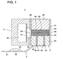
- Fig. 1 is a drawing showing a printing unit equipped with an ink jet head of a chevron type
- Fig. 2 is a drawing showing the outside-leading of drive electrodes of an ink jet head of a chevron type.
- the printing unit 1 of this embodiment comprises the ink jet head 2, the ink supply portion 3, and the drive portion 4.
- the ink jet head 2 comprises the piezoelectric elements 20 and 21, the printed circuit board 22, the cover member 23, the nozzle plate 24, and the partition sheet 25.
- the ink chambers 26 and the air chambers 27 are alternately formed in the piezoelectric elements 20 and 21, the nozzle holes 28 are formed at the positions corresponding to the ink chambers 26 in said nozzle plate, and the ink supply holes 29 are formed at the positions corresponding to the ink chambers in the partition sheet 25.
- the ink pool 30 from which ink is conducted to the ink supply holes 29 through the ink filter 31 and the ink supply paths 32.
- the through-holes 40 are formed at the positions corresponding to the ink chambers 26 and the air chambers 27, and in these through-holes 40, the lead conductors 41 are provided.
- the drive electrodes 50 are provided, and these drive electrodes are provided throughout the holes to the bottom to be connected to the outside lead wires 42 which are provided on the printed circuit board 22.
- the drive circuit board 51 which is made up of a flexible wiring board and is connected to the outside lead wires 42.
- the drive circuit 52 is built on the drive circuit board 51, and is made up of a drive IC.
- the drive circuit 52 is covered by the protective sheet 53.
- the lead conductors 41 are provided beforehand in the through-holes 40 of the printed circuit board 22, while the piezoelectric element 20 and the piezoelectric element 21 are bonded, and the piezoelectric element 20 is bonded to the printed circuit board 22.
- slots are formed with a predetermined interval from the side of the piezoelectric elements 20 and 21, to carry out the working for forming the ink chambers 26 and the air chambers 27 alternately.
- the surface of the printed circuit board 22 is slightly shaved, to expose the lead conductors 41 in the through-holes 40.
- the drive electrodes 50 are formed on the partition walls 20a and 21a which partition the ink chambers 26 and the air chambers 27, and the lead conductors 41 are connected to these drive electrodes 50.
- the cover member 23 is bonded to the piezoelectric element 21, and further, the nozzle plate 24 and the partition sheet 25 are bonded respectively to the both sides of the abovementioned bonded members to close the ink chambers 26 and the air chambers 27.
- gold, silver, aluminum, palladium, nickel, tantalum, and titanium can be used, and in particular, gold and aluminum are good in view of electrical properties and workability; they are formed by plating, evaporation, and sputtering.
- the lead conductors such that the through-holes 40 in the print wiring board 22 is filled with a metal paste of electrode by a screen printing and the filled metal paste is dried.
- the board 22 is manufactured such that a plurality of ceramics green sheets are superimposed and sintered, it may be preferable that the through-holes 40 in the print wiring board 22 is filled with a metal paste of electrode by a screen printing before the sintering.
- the drive electrodes 50 such that aluminum is deposited on wall surfaces of grooves provided in the piezoelectric elements 20 and 21 by the vapor deposition in an oblique direction.
- an aluminum layer is formed on the surface of the exposed lead conductors 41, thereby automatically constructing a firm connection between the drive electrodes 50 and the lead conductors 41.
- the drive electrodes 50 is formed by no-electric filed plating of Ni and Au
- the connection between the drive electrodes 50 and the lead conductors 41 is also firmly constructed.
- a portion on which no plating layer is required can be formed by a masking tape or by eliminating a plating layer by a laser cutting.
- ink is supplied from the ink tank 30 in the ink supply portion 3 to the ink chambers 26 through the ink supply holes 29 in the ink jet head 2, and the ink supply holes 29 are formed at the positions opposite to the nozzle holes 28.
- the partition walls 20a and 21a which partition the ink chambers 26 and the air chambers 27 are shear-deformed to jet the ink in the ink chambers 26 from the nozzle holes 28.
- the drive electrodes 50 are connected to the lead conductors 41 from the drive circuit 52, said lead conductors 41 being provided at the bottom side of the ink chambers 26 and the air chambers 27, and the drive electrodes 50 are connected to the outside drive circuit 52 at the positions directly beneath the drive portions; hence, the electrostatic capacitance owing to the connection can be neglected, and the amount of heat generation is small, to make it possible to reduce the weight of the power source for driving; thus, a line head with highly integrated nozzles capable of carrying out a high quality image recording can be actualized, and the power source of the printing unit is made small-sized and to have a small output power. Further, the outside-leading of the drive electrodes 50 is simple and reliable, to make a high-speed, high-definition, and high-quality small-sized printing unit, which is of low cost and compact.
- the printed circuit board 22 is used for the wiring from the drive circuit 52, the piezoelectric elements 20 and 21 are provided on this printed circuit board 22, the ink chambers 26 and the air chambers 27 are formed at the positions agreeing with the wiring positions in such a manner as to make the lead conductors 41 exposed, and the drive electrodes 50 are connected to the lead conductors 41 at the time of forming said drive electrodes 50 on the partition walls 20a and 20b; hence, a process such as wire bonding or soldering as is heretofore done is not required, and the connection to the lead conductors 41 from the drive circuit 52 can be made simultaneously at the time of attaching the drive electrodes 50, to make it possible to omit the wiring process; thus, the outside-leading of the drive electrodes 50 is simple and reliable, to make the ink jet head of low cost and compact.
- the printed circuit board 22 is made of a material having a Young's modulus larger than that of the piezoelectric elements 20 and 21, for example, made of a non-piezoelectric ceramics material; hence, the piezoelectric element can be reliably supported even when the partition walls 20a and 21a of the ink chambers 26 and the air chambers 27 are shear-deformed.
- the non-piezoelectric ceramics material is at least any one selected from alumina, aluminum nitride, zirconia, silicon, silicon nitride, silicon carbide, and quartz; hence, the piezoelectric element can be reliably supported.
- the surface of the printed circuit board 22 to make the bottom of the ink chambers is a smooth surface; hence, the thickness of the adhesive layer to bond the printed circuit board 22 and the piezoelectric element 20 can be made thin, and the both rigid bodies can be held together, to make the jetting efficiency high.
- the printed circuit board 22 is connected to the drive circuit board 51 which is separately provided to the printed circuit board 22, and the drive circuit 52 is built on said drive circuit board 51; hence, the ease of operation for attaching the drive circuit 52 is improved and the degree of freedom in designing is enlarged.
- cover member 23 is made of a non-piezoelectric ceramics material, and for example, aluminum is used for this non-piezoelectric ceramics material.
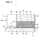
- FIG. 3 is a drawing showing a printing unit equipped with an ink jet head of a chevron type
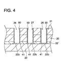
- Fig. 4 is a drawing showing the outside-leading of the drive electrodes of an ink jet head of a chevron type.
- the two boards of the thick printed circuit board 22 and the thin printed circuit board 22 are stacked, and on this thin printed circuit board 22, the concave portions 22b are formed at the positions corresponding to the ink chambers 26 and the air chambers 27, and in this concave portions 22b, the lead conductors 41 are formed.
- the piezoelectric elements 20 and 21 are worked for the slots to form the ink chambers 26 and the air chambers 27 at the positions agreeing with the wiring positions in such a manner as to make the lead conductors 41 exposed, and the drive electrodes are connected to the lead conductors 41 when they are formed on the partition walls 20a and 21a.
- the drive circuit 52 is built on the thick printed circuit board 22, and is connected to the lead conductors 41; thus, the drive circuit 52 is connected to the drive electrodes 50 through the lead conductors 41.
- a pattern electrode 41 can be easily precisely provided on the thick board having a thickness of 0.3 mm to 3 mm at low cost.
- concaves 22b in the thin board having a thickness of 0.05 mm to 0.3 mm and pasting the thin board with a piezoelectric element, a connection between a lead conductor 41 and a drive electrode 50 can be made firmly and easily.
- the drive circuit 52 is built on the printed circuit board 22 and is connected to the drive electrodes 50; hence, the outside-leading of the drive electrodes 50 is simple and reliable to make an ink jet head of low cost and compact.
- FIG. 5 is a drawing showing a printing unit equipped with an ink jet head of a chevron type.
- the lead wires 55 are formed on the opposite side to the drive electrodes 50 on the printed circuit board 22, and are connected to the drive circuit 52 built on the printed circuit board 22.
- the lead wires 55 are connected to the lead conductors 41 which are provided in the through-holes 40 of the printed circuit board 22.
- the outside lead wires 56 are connected to the drive circuit 52, and the flexible board 57 is connected to these outside lead wires 57, which are connected to the external control portion etc.
- the drive circuit 52 is built on the printed circuit board 22, and is connected to the drive electrodes 50; hence, the outside-leading of the drive electrodes 50 is simple and reliable, to make the ink jet head of low cost and compact.
- Fig. 6(a) is the plan of an ink jet head of a chevron type
- Fig. 6(b) is a cross-sectional view of the ink jet head of a chevron type.
- the lead wires 57 are formed on the opposite side to the drive electrodes 50 on the printed circuit board 22, and are connected to the drive circuit 52 built on the printed circuit board 22.
- the lead wires 57 are connected to the lead conductors 41 which are provided in the through-holes 40 of the printed circuit board 22.
- the outside lead wires 58 are connected to the drive circuit 52.
- the lead wires 57 and the outside lead wires 58 are connected through the anisotropic conductive film 59, the drive circuit 52 is built on the printed circuit board 22, and the drive electrodes 50 are connected to this drive circuit 52; hence, the outside-leading of the drive electrodes is simple and reliable, to make the ink jet head of low cost and compact.
- Fig. 7 is a cross-sectional view of an ink jet head of a chevron type.
- the printed circuit board is made up of multiple layers, that is, three layers, and the through-holes are provided in this printed circuit board 22 made up of three layers, and the lead conductors 41 provided in these through-holes 40 are connected to the drive electrodes 50.
- the drive IC making up the drive circuit 52 is buried between the bottom layer and the intermediate layer of the printed circuit board 22. Further, in the intermediate layer of the printed circuit board 22, the resistors 80 and the capacitors 81 are buried; further, in the bottom and intermediate layers of the printed circuit board 22, the connecting wires 48 are provided, and the connector 82 is fitted to one of the connecting wires 48 on the bottom layer of the printed circuit board 22.
- the lead conductors 41a is connected with an electrode pattern (not illustrated) provided on a joint surface A between boards 22a and 22b and further connected through a conductor 48 with an electrode pattern (not illustrated) provided on a joint surface B between boards 22b and 22c, whereby the lead conductors 41a is connected with a driving IC 52 embedded in the circuit board 22c.
- the printed circuit board 22 is made up of multiple layers, and the drive IC making up the drive circuit is buried in the printed circuit board 22 made up of multiple layers; hence, the driving circuit including all electric components such as a driving IC, a resister, a capacitor, a thermister, a coil and a connector, necessary for driving the print head may be constructed in a single body, thereby making the outside-leading of the drive electrodes simple and making the print head in compact with a high reliability.
- Fig. 8 is a drawing showing a printing unit equipped with an ink jet head of a chevron type.
- the members which are given the same signs respectively as those in Fig. 1 and Fig. 2 are made up in the same way; therefore, the explanation for them will be omitted.
- the ink supply paths 70 leading to the ink chambers 26 are formed in the printed circuit board 22, and the ink supply conduit 72 formed in the ink supply member 71 is connected to these ink supply paths 70, and further, the ink tube 73 is connected to the ink supply conduit 72.
- the diameter of these ink supply paths 70 is desirably 10 to 500 ⁇ m, or should more desirably be 100 to 200 ⁇ m. Further, the inner wall of the ink supply paths 70 is covered by an organic protective layer, in order that the printed circuit board should not be corroded by the ink. As described in the above, the ink supply paths 70 leading to the ink chambers 26 are formed in the printed circuit board 22; hence, the piping for supplying ink is made easy.
- Fig. 9(a) is the plan of the printed circuit board
- Fig. 9(b) is a cross-sectional view of the printed circuit board
- Fig. 9(c) is the bottom view of the printed circuit board.
- the thickness of the board is 0.635 mm.
- the line pitch is 140 ⁇ 5 ⁇ m
- the wiring pitch of the through-holes is 140 ⁇ 5 ⁇ m
- the width of the line is 70 ⁇ 10 ⁇ m
- the diameter of the wires in the through-holes is 70 ⁇ 5 ⁇ m.
- the LTCC non-contracting board for example, DU PON GREEN TAPE #951 is used.
- the contraction ratio is not larger than 0.1 ⁇ 0.005%, and the precision of the wiring pattern is ⁇ 1 to ⁇ 5 ⁇ m in terms of accumulated positional deviation.
- the smoothness is better than (10 ⁇ m)/(10 mm), and the board is able to be bonded by an adhesive, has enough bonding strength, and is sensitive to a piezoelectric element.
- the LTCC non-contracting board is capable of multi-layer wiring, in which resistors and capacitors are buried in the circuit board and a drive IC can be provided in a concave portion made by boring.
- the smoothness is not larger than (10 ⁇ m)/(10 mm)
- a surface roughness is measured by a contact stylus instrument (or contact profile meter, such as an instrument produced by Taristep Corporation)
- a surface roughness Ra is not larger than 10 ⁇ m with a measuring width of 10 mm in any optional direction.
- the dielectric constant is 7.8 at 10 MHz
- the coefficient of thermal expansion is preferably not larger than 10 ppm/deg, more preferably not larger than 6 ppm/deg
- the thermal conductivity is 30 w/m-deg
- the Young's modulus is 200GPa.
- the thickness of the pattern conductor is not larger than 30 ⁇ m, or should desirably be not larger than 10 ⁇ m, or should more desirably be not larger than 5 ⁇ m, at which bonding by an adhesive is possible.
- the ink jet heads of a chevron type have been explained; however, this invention can be brought into practice in an ink jet head of a cantilever type in the same manner. Further, the embodiments wherein the ink chambers and the air chambers are alternately formed have been explained; however, this invention can be put into practice in an ink jet head having ink chambers formed without providing air chambers.
- the material of the non-piezoelectric ceramics substrate it is desirable to select at least one out of alumina, aluminum nitride, zirconia, silicon, silicon nitride, silicon carbide, and quartz; thus, the piezoelectric ceramics can be reliably supported by it even when the partition walls of the ink chambers are deformed by a shearing force.
- a ceramics material such as PZT and PLZT, which is composed of a mixture of micro-crystalline PbOx, ZrOx, and TiOx including a minute amount of a metallic oxide which is known as a softening agent or a hardening agent such as, for example, an oxide of Nb, Zn, Mg, Sn, Ni, La, or Cr.
- PZT is the mixture of lead titanate and lead zirconate, and it is a desirable material owing to a large packing density, a large piezoelectric constant, and a good workability.
- PZT has its crystalline structure suddenly varied to make the atoms deviate, and becomes an aggregate of micro-crystals in the form of dipoles each having a positive pole at one end and a negative pole at the other end. In such spontaneous polarization, dipoles have random directions to cancel their dipole moment one another; therefore, a further polarizing process is required.
- a thin plate of PZT is placed between electrodes, is dipped in a silicone oil, and is polarized by the application of a high electric field in the range of 10 to 35 kV/cm.
- a high electric field in the range of 10 to 35 kV/cm.
- the density [g/cm 3 ] of the piezoelectric ceramics is 8.2, and the density [g/cm 3 ] of the non-piezoelectric ceramics substrate is let to be equal to or smaller than 3.0; however, the density [g/cm 3 ] of the non-piezoelectric ceramics substrate should desirably be smaller, for example, equal to or smaller than a half of the above; thus, the head as a whole becomes lighter to make it possible to obtain a compact head.
- the Young's modulus or the elastic constant [GPa] of the piezoelectric ceramics is 6.5, and the Young's modulus [GPa] of the non-piezoelectric ceramics substrate is let to be 190 to 390; however, the Young's modulus [GPa] of the non-piezoelectric ceramics substrate should desirably be larger, for example, equal to or larger than 200; thus, it can support the displacement of the partition wall of the piezoelectric ceramics firmly, and can make an efficient driving to enable the lowering of applied voltage owing to the small deformation of itself.
- the thermal expansion coefficient [ppm/deg] of the piezoelectric ceramics is 2.0, and the thermal expansion coefficient [ppm/deg] of the non-piezoelectric ceramics substrate is let to be 0.6 to 7.0; however, the difference between the both should desirably be equal to or smaller than 5.0, or more desirably should be equal to or smaller than 3.0; thus, it can be prevented the breakdown by the bending and the stress owing to the difference between the thermal expansions of the substrates which are caused to occur by the heat generation in driving and with the variation of the environment temperature.
- the thermal conductivity [W/cm ⁇ deg] of the piezoelectric ceramics is 0.01, and the thermal conductivity [W/cm ⁇ deg] of the non-piezoelectric ceramics substrate is let to be 0.03 to 0.3; however, the thermal conductivity [W/cm ⁇ deg] of the non-piezoelectric ceramics substrate should desirably be larger, and it becomes more desirable the larger it is, because the heat generated in driving the piezoelectric ceramics can be let to dissipate to the outside through the non-piezoelectric ceramics substrate.
- the dielectric constant of the piezoelectric ceramics is 3,000 and the dielectric constant of the non-piezoelectric ceramics substrate is let to be 4.0 to 50; however, it becomes more desirable the smaller it is, and it should desirably be equal to or smaller than 10; further, by putting the electrode pattern for driving the piezoelectric ceramics on the non-piezoelectric ceramics substrate, an additional capacitance is produced on top of the capacitance of the piezoelectric ceramics itself; hence, the capacitance of the ink chamber is increased to cause the heat generation to increase and the driving efficiency to decrease. In this case, the additional capacitance can be made smaller, the smaller the dielectric constant of the non-piezoelectric ceramics becomes.
- the hardness [Hv] of the piezoelectric ceramics is 500, and the hardness [Hv] of the non-piezoelectric ceramics substrate is let to be equal to or larger than 1,000; however, the hardness [Hv] of the non-piezoelectric ceramics substrate should desirably be larger, that is, should desirably be equal to or larger than 1.5 times the above value; thus, the lowering of the yield owing to the breaking in the manufacturing process can be prevented.
- the bending strength [Kgf/cm 2 ] of the piezoelectric ceramics is 1,000, and the bending strength [Kgf/cm 2 ] of the non-piezoelectric ceramics substrate is let to be 3,000 to 9,000; however, the bending strength [Kgf/cm 2 ] of the non-piezoelectric ceramics substrate should be larger, that is, should desirably be equal to or larger than 2 times the above value, because a long-sized ink jet head can be more stably manufactured the stronger against the warping and bending the non-piezoelectric substrate is.
- the volume resistivity [ ⁇ cm] of the piezoelectric ceramics is 1, and the volume resistivity [ ⁇ cm] of the non-piezoelectric ceramics substrate is let to be 7 to 10; however, the volume resistivity [ ⁇ cm] of the non-piezoelectric ceramics substrate should desirably be larger, that is, it is better the larger it is in order to decrease the leakage current as an electronic device.
- the surface roughness Ra of the bonding surfaces between the non-piezoelectric ceramics substrate and the piezoelectric ceramics is equal to or smaller than 1.0 ⁇ m, and should desirably be equal to or smaller than 0.3 ⁇ m, or more desirably should be equal to or smaller than 0.1 ⁇ m; if the surface roughness Ra exceeds 1.0 ⁇ m, an excessive amount of a soft high-molecular adhesive (an epoxy adhesive, for example) is injected between the bonding surfaces to cause the driving force of the piezoelectric ceramics to be lowered, and it is not desirable to bring about the lowering of the sensitivity and the up-rising of the required electric voltage.
- a soft high-molecular adhesive an epoxy adhesive, for example
- the bonding surfaces between the non-piezoelectric ceramics substrate and the piezoelectric ceramics are subjected to a plasma processing or a UV processing.
- the plasma processing is a processing in which the non-piezoelectric substrate or the piezoelectric ceramics is placed in a vacuum chamber, and any one or the mixture of Ar, N 2 , and O 2 gases, is introduced in it, and is brought into the state of plasma by the electromagnetic field applied from the outside; a fluorinated hydrocarbon gas such as CF 4 may be used in order to enhance the susceptibility to etching of the surfaces.
- the UV processing is a processing in which the non-piezoelectric ceramics substrate or the piezoelectric ceramics is directly irradiated by an ultra-violet ray emitting lamp, and it may be carried out in an O 2 environment in order to produce a cleaning effect by ozone.
- the ink jet head comprises ink chambers 26 and air chambers 27.
- the present invention can be applied to an embodiment in which an ink head has not air chamber 27 and ink chambers are driven in 3-cycle mode.
- the drive electrodes are connected to the lead conductors from the drive circuit provided at the bottom side of the ink chambers, that is, connected to the outside drive circuit at the positions directly beneath the driving portions; hence, the electrostatic capacitance owing to the connection can be neglected to generate only a small amount of heat, and drive electrodes can be made light-weighted and small-sized.
- a line head with highly integrated nozzles which is capable of being driven at a high speed and is capable of making a high-quality image recording can be actualized, and the power source of a printing unit equipped with the ink jet head can be made small-sized and of small rated power.
- the outside-leading of the drive electrodes is simple and reliable, to make a small-sized printing unit which is of low cost and compact, works at high speed and records an image of a high definition and high quality.
- the piezoelectric element is provided on the printed circuit board, the ink chambers are formed at the positions agreeing with the wiring positions in such a manner as to make the lead conductors exposed, and the drive electrodes are connected to the lead conductors at the time of forming said drive electrodes on the partition walls; hence, a process such as wire bonding or soldering as is heretofore done is not required, and the connection to the lead conductors from the drive circuit can be made simultaneously at the time of attaching the drive electrodes, to make it possible to omit the wiring process; thus, the outside-leading of the drive electrodes is simple and reliable, to make the ink jet head of low cost and compact.
- the printed circuit board has through-holes at the positions corresponding to the ink chambers, and the drive electrodes are connected to the lead conductors provided in these through-holes; hence, it is prevented that the wiring pattern of the printed circuit board is shaved off to make a poor connection at the time of working the ink chambers owing to the error in the depth of working.
- the printed circuit board is made of a material having a Young's modulus larger than that of the piezoelectric element; hence, the piezoelectric element can be reliably supported even when the partition walls of the ink chambers are shear-deformed.
- the printed circuit board is made of a non-piezoelectric ceramics material; hence, the piezoelectric element can be reliably supported even when the partition walls of the ink chambers are shear-deformed.
- the non-piezoelectric ceramics material is at least any one selected from alumina, aluminum nitride, zirconia, silicon, silicon nitride, silicon carbide, and quartz; hence, the piezoelectric element can be reliably supported.
- the surface of the printed circuit board to make the bottom of the ink chambers is a smooth surface; hence, the thickness of the adhesive layer to bond the printed circuit board and the piezoelectric element can be made thin, and the both rigid bodies can be held together, to make the jetting efficiency high.
- the printed circuit board is connected to a drive circuit board which is separately provided, and a drive circuit is built on said drive circuit board; hence, the ease of operation for attaching the drive circuit is improved and the degree of freedom in designing is enlarged.
- a drive circuit is built on the printed circuit board, and this drive circuit is connected to the drive electrodes; hence, the outside-leading of the drive electrodes is simple and reliable, and the ink jet head becomes of low cost and compact.
- ink supply paths leading to the aforesaid ink chambers are formed in the aforesaid printed circuit board; hence, it is easy to make a piping work for supplying ink.
- the electrodes are connected to the outside drive circuit at the positions directly beneath the driving portions; hence, the electrostatic capacitance produced by the connection can be neglected to make the power source for driving light-weighted and small-sized, and on top of it, a special connecting process can be omitted because the connection to the lead conductors of the drive circuit can be carried out simultaneously at the time of attaching the drive electrodes.
- the ink jet head is capable of being driven at a high speed, is capable of making a high-quality image recording, has drive electrodes which are led outside in a simple way and reliably, is of low cost, and has a possibility to be made compact.
Landscapes
- Particle Formation And Scattering Control In Inkjet Printers (AREA)
Abstract
Description
Claims (13)
- An ink jet head, comprising:partition walls made of an piezoelectric material and for dividing ink chambers; anddriving electrodes provided on the partition walls, wherein lead conductors each of which is provided at a bottom portion of each ink chamber and is connected with a driving circuit, each lead conductor connected with the driving electrode so that a voltage is applied from the driving circuit through the lead conductor to the driving electrodes for each ink chamber, whereby the partition walls are deformed by shearing forces and an ink is jetted from each ink chamber.
- The ink jet head of claim 1, further comprising:a printed circuit board electrically connected with the driving circuit, wherein the partition walls are mounted on the printed circuit board so that the printed circuit board constitutes the bottom portions of the ink chambers, and wherein the lead conductors are provided on the printed circuit board at positions corresponding to the bottom portions of the ink chambers.
- The ink jet head of claim 1, wherein the printed circuit board is provided with through-holes at the positions corresponding to the bottom portions of the ink chambers, each lead conductor provided at the bottom portion for each ink chamber is connected with a through-electrode provided in each through-hole, and the through-electrode is connected with the each driving electrode.
- The ink jet head of claim 1, wherein the printed circuit board is made of a material having a Young's modulus larger than that of the piezoelectric element.
- The ink jet head of claim 1, wherein the printed circuit board is made of a non-piezoelectric ceramics material.
- The ink jet head of claim 5, wherein the non-piezoelectric ceramics material is at least one of alumina, aluminum nitride, zirconia, silicon, silicon nitride, silicon carbide, and quartz.
- The ink jet head of claim 1, wherein at least a surface of the printed circuit board constituting the bottom surface of the ink chamber is a smoothed surface.
- The ink jet head of claim 2, further comprising:a driving circuit board provided separately from the printed circuit board and electrically connected with the printed circuit board, wherein the driving circuit is provided on or in the driving circuit board.
- The ink jet head of claim 2, wherein the driving circuit is provided on the printed circuit board and is connected with the driving electrodes through the lead conductors.
- The ink jet head of claim 2, wherein an ink feeding passage communicating with the ink chambers is formed in the printed circuit board.
- The ink jet head of claim 1, wherein each lead conductor is connected with each driving electrode at the bottom portion of each ink chamber.
- The ink jet head of claim 1, wherein the partition walls are walls for partitioning ink chambers into each ink chamber.
- The ink jet head of claim 2, wherein the lead conductors which are provided unwrappedly on the printed circuit board is electrically connected with the driving electrodes when the driving electrodes is provided on the partition walls.
Applications Claiming Priority (2)
| Application Number | Priority Date | Filing Date | Title |
|---|---|---|---|
| JP3814299 | 1999-02-17 | ||
| JP3814299 | 1999-02-17 |
Publications (3)
| Publication Number | Publication Date |
|---|---|
| EP1029678A2 true EP1029678A2 (en) | 2000-08-23 |
| EP1029678A3 EP1029678A3 (en) | 2000-12-27 |
| EP1029678B1 EP1029678B1 (en) | 2008-04-09 |
Family
ID=12517178
Family Applications (1)
| Application Number | Title | Priority Date | Filing Date |
|---|---|---|---|
| EP00103149A Expired - Lifetime EP1029678B1 (en) | 1999-02-17 | 2000-02-16 | Ink jet head |
Country Status (3)
| Country | Link |
|---|---|
| US (1) | US6568797B2 (en) |
| EP (1) | EP1029678B1 (en) |
| DE (1) | DE60038514D1 (en) |
Cited By (5)
| Publication number | Priority date | Publication date | Assignee | Title |
|---|---|---|---|---|
| GB2362609A (en) * | 2000-05-25 | 2001-11-28 | Seiko Instr Inc | Method of manufacturing a piezoelectric inkjet printhead including wiring lines having an inorganic conductive film as a lowest layer and metal films thereon |
| WO2002026501A1 (en) * | 2000-09-26 | 2002-04-04 | Xaar Technology Limited | Droplet deposition apparatus |
| EP1598191A2 (en) | 2004-05-19 | 2005-11-23 | Brother Kogyo Kabushiki Kaisha | Piezoelectric actuator, ink-jet head provided with the same, ink-jet printer and method for manufacturing piezoelectric actuator |
| EP1645417A1 (en) * | 2004-10-05 | 2006-04-12 | Brother Kogyo Kabushiki Kaisha | An ink jet head |
| CN105984218A (en) * | 2015-03-16 | 2016-10-05 | 精工爱普生株式会社 | Electronic device |
Families Citing this family (20)
| Publication number | Priority date | Publication date | Assignee | Title |
|---|---|---|---|---|
| JP2001334673A (en) * | 2000-05-26 | 2001-12-04 | Seiko Instruments Inc | Manufacturing method of head chip |
| US6848773B1 (en) * | 2000-09-15 | 2005-02-01 | Spectra, Inc. | Piezoelectric ink jet printing module |
| US7052117B2 (en) | 2002-07-03 | 2006-05-30 | Dimatix, Inc. | Printhead having a thin pre-fired piezoelectric layer |
| US20040051762A1 (en) * | 2002-09-12 | 2004-03-18 | Nishi Shin-Ichi | Inkjet recording head |
| US7097286B2 (en) * | 2003-11-12 | 2006-08-29 | Kyocera Corporation | Ink jet recording head structure, ink jet printer, powder molding method, method of manufacturing recording head structure supporting member, and powder molding press apparatus |
| GB2410463A (en) * | 2004-01-29 | 2005-08-03 | Hewlett Packard Development Co | A method of making an inkjet printhead |
| US7281778B2 (en) | 2004-03-15 | 2007-10-16 | Fujifilm Dimatix, Inc. | High frequency droplet ejection device and method |
| US8491076B2 (en) | 2004-03-15 | 2013-07-23 | Fujifilm Dimatix, Inc. | Fluid droplet ejection devices and methods |
| JP4135697B2 (en) * | 2004-09-30 | 2008-08-20 | 富士フイルム株式会社 | Liquid ejection head and image forming apparatus |
| US7420317B2 (en) * | 2004-10-15 | 2008-09-02 | Fujifilm Dimatix, Inc. | Forming piezoelectric actuators |
| US7388319B2 (en) * | 2004-10-15 | 2008-06-17 | Fujifilm Dimatix, Inc. | Forming piezoelectric actuators |
| KR20070087223A (en) | 2004-12-30 | 2007-08-27 | 후지필름 디마틱스, 인크. | Inkjet printing |
| JP4995470B2 (en) * | 2005-07-20 | 2012-08-08 | エスアイアイ・プリンテック株式会社 | Inkjet head and inkjet recording apparatus |
| US7665828B2 (en) * | 2006-09-21 | 2010-02-23 | Xerox Corporation | Drop generator |
| US7988247B2 (en) | 2007-01-11 | 2011-08-02 | Fujifilm Dimatix, Inc. | Ejection of drops having variable drop size from an ink jet printer |
| US7681991B2 (en) * | 2007-06-04 | 2010-03-23 | Lexmark International, Inc. | Composite ceramic substrate for micro-fluid ejection head |
| JP5309686B2 (en) * | 2008-05-14 | 2013-10-09 | コニカミノルタ株式会社 | Inkjet head |
| JP5304021B2 (en) * | 2008-05-14 | 2013-10-02 | コニカミノルタ株式会社 | Inkjet head manufacturing method |
| US10654269B2 (en) * | 2017-06-28 | 2020-05-19 | Canon Kabushiki Kaisha | Liquid ejection head |
| GB2599902A (en) * | 2020-10-11 | 2022-04-20 | Mesa Tech Ltd | Printing apparatus and method |
Family Cites Families (19)
| Publication number | Priority date | Publication date | Assignee | Title |
|---|---|---|---|---|
| US4791440A (en) * | 1987-05-01 | 1988-12-13 | International Business Machine Corporation | Thermal drop-on-demand ink jet print head |
| GB8824014D0 (en) * | 1988-10-13 | 1988-11-23 | Am Int | High density multi-channel array electrically pulsed droplet deposition apparatus |
| US4940995A (en) * | 1988-11-18 | 1990-07-10 | Spectra, Inc. | Removal of dissolved gas from ink in an ink jet system |
| GB9113023D0 (en) * | 1991-06-17 | 1991-08-07 | Xaar Ltd | Multi-channel arrary droplet deposition apparatus and method of manufacture thereof |
| CA2075097C (en) * | 1991-08-02 | 2000-03-28 | Hiroyuki Ishinaga | Recording apparatus, recording head and substrate therefor |
| JP2749475B2 (en) * | 1991-10-04 | 1998-05-13 | 株式会社テック | Method of manufacturing ink jet printer head |
| US5518969A (en) * | 1992-06-22 | 1996-05-21 | Ragan; Randall C. | Process for producing low shrink ceramic composition |
| JP3151644B2 (en) * | 1993-03-08 | 2001-04-03 | 日本碍子株式会社 | Piezoelectric / electrostrictive film type element |
| JPH07243064A (en) * | 1994-01-03 | 1995-09-19 | Xerox Corp | Cleaning method for substrate |
| DE69525821T2 (en) | 1994-12-16 | 2002-09-19 | Compaq Computer Corp., Houston | On-demand ink jet print head with an elongated channel for ejecting orthogonally directed droplets with improved working speed |
| JPH08192514A (en) * | 1995-01-19 | 1996-07-30 | Brother Ind Ltd | Ink jet recording device |
| US5818481A (en) * | 1995-02-13 | 1998-10-06 | Minolta Co., Ltd. | Ink jet printing head having a piezoelectric driver member |
| US5997135A (en) | 1995-03-27 | 1999-12-07 | Brother Kogyo Kabushiki Kaisha | Two actuator shear mode type ink jet print head with dimensional relations |
| JPH09207331A (en) | 1996-02-07 | 1997-08-12 | Matsushita Electric Ind Co Ltd | Inkjet recording head |
| US5762812A (en) * | 1996-05-02 | 1998-06-09 | Xerox Corporation | Thermal ink jet printhead and process for preparation thereof |
| JPH1076669A (en) | 1996-09-03 | 1998-03-24 | Matsushita Electric Ind Co Ltd | Method of manufacturing ink jet recording head |
| JPH10146974A (en) * | 1996-11-19 | 1998-06-02 | Brother Ind Ltd | Inkjet head |
| GB2338927B (en) * | 1998-07-02 | 2000-08-09 | Tokyo Electric Co Ltd | A driving method of an ink-jet head |
| US6205032B1 (en) * | 1999-03-16 | 2001-03-20 | Cts Corporation | Low temperature co-fired ceramic with improved registration |
-
2000
- 2000-02-16 EP EP00103149A patent/EP1029678B1/en not_active Expired - Lifetime
- 2000-02-16 US US09/505,137 patent/US6568797B2/en not_active Expired - Fee Related
- 2000-02-16 DE DE60038514T patent/DE60038514D1/en not_active Expired - Lifetime
Cited By (18)
| Publication number | Priority date | Publication date | Assignee | Title |
|---|---|---|---|---|
| US6491383B2 (en) | 2000-05-25 | 2002-12-10 | Seiko Instruments Inc. | Head chip and head unit |
| GB2362609B (en) * | 2000-05-25 | 2004-01-07 | Seiko Instr Inc | Head chip and head unit |
| GB2362609A (en) * | 2000-05-25 | 2001-11-28 | Seiko Instr Inc | Method of manufacturing a piezoelectric inkjet printhead including wiring lines having an inorganic conductive film as a lowest layer and metal films thereon |
| US7178906B2 (en) | 2000-09-26 | 2007-02-20 | Xaar Technology Limited | Droplet deposition apparatus |
| WO2002026501A1 (en) * | 2000-09-26 | 2002-04-04 | Xaar Technology Limited | Droplet deposition apparatus |
| CN100376396C (en) * | 2004-05-19 | 2008-03-26 | 兄弟工业株式会社 | Piezoelectric mechanism, manufacturing method thereof, inkjet head, and inkjet printer |
| EP1598191A3 (en) * | 2004-05-19 | 2006-11-02 | Brother Kogyo Kabushiki Kaisha | Piezoelectric actuator, ink-jet head provided with the same, ink-jet printer and method for manufacturing piezoelectric actuator |
| EP1598191A2 (en) | 2004-05-19 | 2005-11-23 | Brother Kogyo Kabushiki Kaisha | Piezoelectric actuator, ink-jet head provided with the same, ink-jet printer and method for manufacturing piezoelectric actuator |
| US7479729B2 (en) | 2004-05-19 | 2009-01-20 | Brother Kogyo Kabushiki Kaisha | Piezoelectric actuator, ink-jet head provided with the same, ink-jet printer, and method for manufacturing piezoelectric actuator |
| US7732989B2 (en) | 2004-05-19 | 2010-06-08 | Brother Kogyo Kabushiki Kaisha | Piezoelectric actuator with terminals on common plane, ink-jet head provided with the same, ink-jet printer, and method for manufacturing piezoelectric actuator |
| US8732921B2 (en) | 2004-05-19 | 2014-05-27 | Brother Kogyo Kabushiki Kaisha | Method for manufacturing piezoelectric actuator |
| US9302467B2 (en) | 2004-05-19 | 2016-04-05 | Brother Kogyo Kabushiki Kaisha | Laminated piezoelectric actuator for an ink-jet head |
| US10340439B2 (en) | 2004-05-19 | 2019-07-02 | Brother Kogyo Kabushiki Kaisha | Method for manufacturing piezoelectric actuator |
| US10978634B2 (en) | 2004-05-19 | 2021-04-13 | Brother Kogyo Kabushiki Kaisha | Method for manufacturing piezoelectric actuator |
| US11711981B2 (en) | 2004-05-19 | 2023-07-25 | Brother Kogyo Kabushiki Kaisha | Piezoelectric actuator |
| EP1645417A1 (en) * | 2004-10-05 | 2006-04-12 | Brother Kogyo Kabushiki Kaisha | An ink jet head |
| US7478896B2 (en) | 2004-10-05 | 2009-01-20 | Kyocera Corporation | Ink jet head |
| CN105984218A (en) * | 2015-03-16 | 2016-10-05 | 精工爱普生株式会社 | Electronic device |
Also Published As
| Publication number | Publication date |
|---|---|
| US20020089574A1 (en) | 2002-07-11 |
| EP1029678B1 (en) | 2008-04-09 |
| DE60038514D1 (en) | 2008-05-21 |
| EP1029678A3 (en) | 2000-12-27 |
| US6568797B2 (en) | 2003-05-27 |
Similar Documents
| Publication | Publication Date | Title |
|---|---|---|
| US6568797B2 (en) | Ink jet head | |
| JP3362733B2 (en) | Ink jet recording device | |
| US5818482A (en) | Ink jet printing head | |
| EP0616890B1 (en) | Ink jet head and method of manufacturing ink jet head | |
| US7159971B2 (en) | Multi-nozzle ink jet head | |
| HK1005905B (en) | Ink jet head and method of manufacturing ink jet head | |
| JP2017124540A (en) | Wiring board, mems device, and liquid jet head | |
| US10625503B2 (en) | Liquid ejection head, liquid ejection apparatus, and electronic device | |
| US8672458B2 (en) | Liquid ejecting head and liquid ejecting apparatus | |
| JP2000301719A (en) | Ink jet head and manufacture thereof | |
| JP7077584B2 (en) | MEMS device, liquid discharge head, and liquid discharge device | |
| CN103287105B (en) | Process for producing liquid ejection head | |
| JP3502743B2 (en) | Ink jet printer head and method of manufacturing the same | |
| JP3575728B2 (en) | Ink jet printer head and method of manufacturing the same | |
| JP4129614B2 (en) | Inkjet recording head and inkjet recording apparatus | |
| JP4645024B2 (en) | Method for manufacturing actuator device | |
| EP1029677A2 (en) | Ink jet head | |
| JP2004284176A (en) | Manufacturing method of liquid jet head | |
| JP6950313B2 (en) | Liquid injection head and liquid injection device | |
| JP2010012724A (en) | Liquid droplet discharge head, image forming apparatus, and method for manufacturing liquid droplet discharge head | |
| JP3166537B2 (en) | Ink jet device | |
| JPH05238009A (en) | INKJET PRINT HEAD AND METHOD OF MANUFACTURING THE SAME | |
| JP2007237718A (en) | Inkjet head manufacturing method | |
| JP2000301722A (en) | Ink jet head | |
| JPH1178010A (en) | Ink jet recording head |
Legal Events
| Date | Code | Title | Description |
|---|---|---|---|
| PUAI | Public reference made under article 153(3) epc to a published international application that has entered the european phase |
Free format text: ORIGINAL CODE: 0009012 |
|
| AK | Designated contracting states |
Kind code of ref document: A2 Designated state(s): DE FR GB |
|
| AX | Request for extension of the european patent |
Free format text: AL;LT;LV;MK;RO;SI |
|
| PUAL | Search report despatched |
Free format text: ORIGINAL CODE: 0009013 |
|
| AK | Designated contracting states |
Kind code of ref document: A3 Designated state(s): AT BE CH CY DE DK ES FI FR GB GR IE IT LI LU MC NL PT SE |
|
| AX | Request for extension of the european patent |
Free format text: AL;LT;LV;MK;RO;SI |
|
| 17P | Request for examination filed |
Effective date: 20010627 |
|
| AKX | Designation fees paid |
Free format text: DE FR GB |
|
| 17Q | First examination report despatched |
Effective date: 20050112 |
|
| 17Q | First examination report despatched |
Effective date: 20050112 |
|
| GRAP | Despatch of communication of intention to grant a patent |
Free format text: ORIGINAL CODE: EPIDOSNIGR1 |
|
| GRAS | Grant fee paid |
Free format text: ORIGINAL CODE: EPIDOSNIGR3 |
|
| GRAA | (expected) grant |
Free format text: ORIGINAL CODE: 0009210 |
|
| AK | Designated contracting states |
Kind code of ref document: B1 Designated state(s): DE FR GB |
|
| REG | Reference to a national code |
Ref country code: GB Ref legal event code: FG4D |
|
| REF | Corresponds to: |
Ref document number: 60038514 Country of ref document: DE Date of ref document: 20080521 Kind code of ref document: P |
|
| EN | Fr: translation not filed | ||
| PLBE | No opposition filed within time limit |
Free format text: ORIGINAL CODE: 0009261 |
|
| STAA | Information on the status of an ep patent application or granted ep patent |
Free format text: STATUS: NO OPPOSITION FILED WITHIN TIME LIMIT |
|
| 26N | No opposition filed |
Effective date: 20090112 |
|
| PG25 | Lapsed in a contracting state [announced via postgrant information from national office to epo] |
Ref country code: DE Free format text: LAPSE BECAUSE OF FAILURE TO SUBMIT A TRANSLATION OF THE DESCRIPTION OR TO PAY THE FEE WITHIN THE PRESCRIBED TIME-LIMIT Effective date: 20080710 Ref country code: FR Free format text: LAPSE BECAUSE OF FAILURE TO SUBMIT A TRANSLATION OF THE DESCRIPTION OR TO PAY THE FEE WITHIN THE PRESCRIBED TIME-LIMIT Effective date: 20090130 |
|
| PGFP | Annual fee paid to national office [announced via postgrant information from national office to epo] |
Ref country code: GB Payment date: 20140212 Year of fee payment: 15 |
|
| GBPC | Gb: european patent ceased through non-payment of renewal fee |
Effective date: 20150216 |
|
| PG25 | Lapsed in a contracting state [announced via postgrant information from national office to epo] |
Ref country code: GB Free format text: LAPSE BECAUSE OF NON-PAYMENT OF DUE FEES Effective date: 20150216 |