The present invention relates to semiconductor device interconnect lines and via
plugs which are fabricated using damascene techniques.
A semiconductor device such as an IC (integrated circuit) generally has electronic
circuit elements such as transistors, diodes and resistors fabricated integrally on a single
body of semiconductor material. The various circuit elements are connected through
conductive connectors to form a complete circuit which can contain millions of individual
circuit elements. Advances in semiconductor materials and processing techniques have
resulted in reducing the overall size of the IC circuit elements while increasing their
number on a single body. Additional miniaturization is highly desirable for improved IC
performance and cost reduction. Interconnects provide the electrical connections between
the various electronic elements of an IC and they form the connections between these
elements and the device's external contact elements, such as pins, for connecting the IC to
other circuits. Typically, interconnect lines form horizontal connections between electronic
circuit elements while conductive via plugs form vertical connections between the
electronic circuit elements, resulting in layered connections.
A variety of techniques are employed to create interconnect lines and via plugs. One
such technique involves a process generally referred to as dual damascene, which includes
forming a trench and an underlying via hole. The trench and the via hole are simultaneously
filled with a conductor material, for example a metal, thus simultaneously forming an
interconnect line and an underlying via plug. Examples of conventional dual damascene
fabrication techniques are disclosed in Kaanta et al., "Dual Damascene: A ULSI Wiring
Technology", Jun. 11-12, 1991, VMIC Conference. IEEE, pages 144-152 and in U.S. Pat.
No. 5,635,423 to Huang et al., 1997.
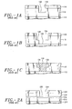
An example of a prior art dual damascene technique is illustrated in FIGS. 1A - 1C,
showing various IC structures. As depicted in FIG. 1A, a dielectric layer 110 is deposited
on a semiconductor substrate 112. An etch mask 116, having a via pattern 118, is
positioned on dielectric layer 110. A timed anisotropic etch is utilized to etch a hole 120 in
layer 110 conforming to the via pattern. Mask 116 is subsequently replaced by mask 122
(FIG. 1B) having a trench pattern 124. A timed anisotropic etch is used to form trench 126
and to simultaneously deepen hole 120 to form via hole 128. This via hole can be etched
to expose semiconductor substrate 112. Alternatively, the via hole can be over-etched
partly into the substrate. As illustrated in FIG. 1C, the via hole and trench are then filled
simultaneously with a suitable metal 130. Metal 130 thus forms a metallized interconnect
line 132 and a via plug 134 which is in contact with semiconductor substrate 112.
Additionally, a liner or barrier layer may be deposited inside the via hole and the trench
prior to deposition of the interconnect metal and the via plug. The surface of layer 110 is
planarized to remove excess metal 130 and to define interconnect line 132. Alternately,
metal etch-back can be utilized to define the line.
Another example of prior art dual damascene is shown in IC structures illustrated
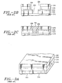
in FIGS. 2A - 2C. As depicted in FIG. 2A, a first dielectric layer 210 is deposited on a
semiconductor substrate 212. An etch stop layer 216, is deposited on first dielectric layer
210. A second dielectric layer 218 is deposited on etch stop 216, and an etch mask 220 is
positioned on dielectric layer 218. Etch mask 220 is patterned (221) for etching a via hole.
Second dielectric layer 218 is etched using a first anisotropic etch procedure, to form a hole
222 (FIG. 2A) conforming to the via pattern. This etching procedure is stopped at etch stop
layer 216. Etch mask 220 is removed and another etch mask 224 (see, FIG. 2B) is
positioned on second dielectric layer 218 such that it is patterned (226) for forming a trench.
A second anisotropic etch procedure is used to etch trench 228 in layer 218.
Simultaneously, hole 222 is extended to substrate 212, by etching through etch stop layer
216 and through first dielectric layer 210. In this dual damascene technique the first etch
procedure has a greater selectivity to etch stop layer 216 than the second etch procedure. As
shown in FIG. 2B, the second etch procedure results in forming trench 228 and via hole 230
which extends to semiconductor substrate 212. Mask 224 is removed, after which trench
228 and via hole 230 are simultaneously filled with a suitable conductive metal 232 (see,
FIG. 2C) forming metallized line 234 and via plug 236 which contacts substrate 212.
Excess metal 232 is removed from the surface of layer 218 to define line 234.
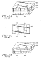
FIGS. 3A - 3I illustrate still another example of a prior art dual damascene
technique. As shown in FIG. 3A, a first dielectric layer 316 is deposited on a substrate 310
which includes interconnect lines 312 and 314. A second dielectric layer 318, providing an
etch stop, is deposited on layer 316. A first mask layer 320 is deposited on the etch stop
layer. Optionally, a cap layer (not shown) may be interposed between the substrate and the
first dielectric layer. Via patterns 322 and 324, see FIG. 3B, are formed in mask layer 320.
As depicted in FIGS. 3B and 3C, via pattern 322 is aligned with line 312 while via pattern
324 is misaligned with line 314. Misalignments, such as via pattern 324, can occur during
the fabrication of IC structures. Via patterns for dual damascene via holes typically have a
square cross sectional configuration such that the width and length of the via pattern are
similar to, or smaller than, the width of the corresponding trench. As used herein, the width
of a via pattern is the dimension which is measured perpendicular to the length dimension
of the corresponding damascene trench pattern for the interconnect line. It is desirable to
form via plugs having cross sectional dimensions which do not exceed the width of the
corresponding interconnect line in order to maximize the number of via plugs which can
be fabricated on, or adjacent to, an interconnect line. While FIGS. 3A - 3I illustrate prior
art structures employing square via patterns, it will be understood that these prior art
techniques are also applicable to via patterns having rounded corners.
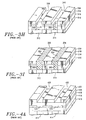
Via patterns 322 and 324 are transferred, by means of anisotropic etching, to etch
stop dielectric layer 318 thereby forming via patterns 326 and 328 respectively, see FIG.
3D. First mask layer 320 is then removed. A third dielectric layer 330 (FIG. 3E) is deposited
on etch stop layer 318 and inside via patterns 326 and 328 of the etch stop layer.
Subsequently, a second mask layer 332 is deposited on third dielectric layer 330. FIG. 3F
shows trench patterns 334 and 336 which are formed in second mask layer 332 such that
these patterns are aligned with substrate interconnect lines 312 and 314 respectively. Trench
patterns 334 and 336 are anisotropically etched through third dielectric layer 330, forming
trenches 338 and 340 respectively, see FIG. 3G. The anisotropic etch also removes third
dielectric layer 330 material from the portions of via patterns 326 and 328 underlying
trenches 338 and 340 respectively. This results in completely opening via pattern 326 (FIG.
3G) which is in good alignment with trench 334. Via pattern 328 is opened only partly due
to the misalignment, forming a reduced via pattern 342 which is not opened across the
entire width of trench 340. Additional anisotropic etching is utilized to etch via patterns 326
and 342 through first dielectric layer 316 to interconnect lines 312 and 314 of substrate 310,
forming via holes 348 and 350. Subsequently, mask layer 332 is removed, as depicted in
FIG. 3H. Alternatively, trenches 338 and 340 (FIG. 3H) can be anisotropically etched (not
shown) through etch stop layer 318. This etching step can also be utilized to simultaneously
anisotropically etch the via holes through a cap layer (not shown) in structures where a cap
layer is interposed between the substrate and the first dielectric layer.
The structure depicted in FIG. 3H includes trenches 338 and 340 extending through
third dielectric layer 330, and via holes 348 and 350 extending through first and second
dielectric layers 316 and 318 respectively. The trenches and via holes are simultaneously
filled with a conductive metal forming dual damascene structures 352 and 354 (FIG. 3J)
which include interconnect lines 356 and 358, and via plugs 360 and 362 respectively. The
prior art technique illustrated in FIGS. 3A - 3I, results in reducing the width of a via hole
compared with the width of the corresponding trench and consequently the width of a via
plug when the via pattern is misaligned with the underlying interconnect line.
The prior art technique which is shown in FIGS. 3A - 3I illustrates a fabrication
sequence wherein the via pattern is misaligned with the underlying interconnect line. These
prior art techniques are also utilized in the structures shown in FIGS. 4A - 4C to illustrate
the effects of misalignment between a trench pattern and the underlying interconnect lines.
FIG. 4A shows a structure which is formed using similar materials and techniques as the
structure depicted in FIG. 3F. The structure shown in FIG. 4A includes substrate 410 having
interconnect lines 412 and 414, first, second (etch stop) and third dielectric layers 416, 418
and 420, and mask layer 422. Via patterns 424 and 426 are aligned with substrate lines 412
and 414 respectively. Mask layer 422 (FIG. 4A) includes trench pattern 428 which is
aligned with line 412 while trench pattern 430 which is misaligned with line 414. FIG. 4B
shows the fabrication of trenches 432 and 434 and via holes 436 and 438 using techniques
similar to those employed to fabricate the trenches and via holes depicted in FIG. 3H. The
trenches and via holes shown in FIG. 4B are simultaneously filled with a conductive metal
forming dual damascene structures 440 and 442, see FIG. 4C. These structures include
interconnect lines 444 and 446, and via plugs 448 and 450. As illustrated in FIGS. 4B and
4C, the prior art technique utilized in the fabrication of these structures results in a reduced
width of the via hole and thus a reduced width of the via plug when the trench pattern is
misaligned with the underlying interconnect line.
Conventional dual damascene techniques, such as those exemplified above, have
shortcomings for meeting the present and future requirements for reduced design rule and
reduced via plug height. For example, the techniques described in connection with FIGS.
1A - 1C utilize a timed etch. As is well known to those of ordinary skill in the art, it is very
difficult to precisely control the etching depth when using a timed etch method. Lack of
precise etching control can cause quality problems. The etch stop techniques described in
connection with FIGS. 2A - 4C provide more etching control than a timed etch. However,
the latter prior art technique requires the use of an etch stop layer between adjacent dual
damascene structures. As is well known to those of ordinary skill in the art, the presence of
an etch stop layer between adjacent dual damascene structures typically results in an
increased capacitance between these structures. Also, prior art techniques such as those
illustrated in FIGS. 3A - 4C can result in reducing the width of the via hole due to
misalignment of the etch patterns. Reduction of the width of the via hole can lead to
incomplete metal fill and to increased resistance of the via plug.
Accordingly, a need exists for cost effective, improved techniques for damascene
fabrication, wherein a power line and a signal line are simultaneously formed.
The present invention provides novel methods and structures for damascene
containing integrated circuit devices which overcome the prior art problems described
above.
In one embodiment of the present invention, a first dielectric layer is deposited on
a substrate, such as a semiconductor substrate. This is followed by the deposition of a
second dielectric layer and a mask layer. A via pattern having a rectangular shape is formed
in the mask layer. The first via pattern is anisotropically etched through the second
dielectric layer, after which the first mask layer is removed. A third dielectric layer is
deposited on the second dielectric layer and inside the via pattern which has been formed
in this layer. Next, a second mask layer having a trench pattern overlaying the via pattern
is formed on the third dielectric layer. The first via pattern is wider than the trench pattern,
to provide misalignment tolerance between the via pattern and the trench pattern. The trench
pattern is anisotropically etched through the third dielectric layer, forming a trench, and
utilizing the second dielectric layer as the etch stop. The trench etching process also
removes the third dielectric layer material from the portion of the first via pattern in the
second dielectric layer which is positioned within the trench pattern, thereby forming a
second via pattern. The second via pattern can only be formed within the trench pattern,
regardless of the width of the original (first) via pattern in the first mask layer. The second
via pattern is then anisotropically etched through the first dielectric layer, thereby forming
a via hole. The via hole and trench are simultaneously filled with a conductive material,
whereby a dual damascene structure is formed. This inventive technique compensates partly
or completely for any misalignment between the via pattern and the trench pattern without
widening the trench at the position of the via hole, thus overcoming prior art dual
damascene fabrication problems associated with misalignment between a via pattern and
the corresponding trench pattern. Advantageously, the present embodiment requires only
two mask layers for the fabrication of misalignment tolerant dual damascene structures.
In another embodiment of the present invention, a dielectric stack is fabricated
which includes an etch stop layer. A portion of the etch stop layer is removed, thereby
forming a gap in the etch stop layer. This gap provides a sacrificial etch segment. Two
adjacent trenches are formed on the etch stop layer such that the sacrificial etch segment is
positioned between the trenches. A via hole is fabricated underneath each trench, wherein
the via hole communicates with the corresponding trench. The via holes and trenches are
simultaneously filled with a conductive material thus fabricating adjacent dual damascene
structures. The sacrificial etch segment between adjacent dual damascene structures forms
a gap in the etch stop layer resulting in lower capacitance between the adjacent dual
damascene structures as compared with conventional techniques which utilize a continuous
etch stop layer between these structures. An example of this novel technique is illustrated
utilizing a dielectric stack having consecutive layers comprising a first dielectric layer
deposited on a substrate, a second dielectric layer providing an etch stop, and a third
dielectric layer. Misalignment can occur between the trench etch patterns and the etch
pattern for the sacrificial etch segment. The present technique provides complete or partial
compensation for such misalignments by positioning adjacent dual damascene trench masks
such that the distance between these masks equals or exceeds the width of the sacrificial
etch segment by a measure which equals or exceeds the extent of the misalignment.
In an additional embodiment of the present invention, the above summarized
embodiments are combined. The combined novel technique provides novel dual damascene
structures which are fabricated using rectangular via patterns where the width of the via
pattern exceeds the width of the connecting overlaying trench, and wherein sacrificial etch
segments are provided between adjacent trenches. The advantages which are realized from
this combined technique include dual damascene structures which are misalignment tolerant
with respect to misalignments between etch mask patterns as well as a reduced capacitance
between adjacent dual damascene structures.
In another embodiment of the present invention, a first dielectric layer is deposited
on a substrate, such as a semiconductor substrate. Second and third dielectric layers are
subsequently deposited, followed by the deposition of a hard mask layer. A first photoresist
layer having a first via pattern is deposited on the hard mask layer. This via pattern, having
a rectangular shape, is wider than the corresponding trench pattern to provide misalignment
tolerance between the via pattern and the trench pattern. The first via pattern is transferred
to the hard mask layer through anisotropic etching, after which the first resist is stripped.
A second resist is deposited on the hard mask layer and inside the via pattern. A trench
pattern overlaying the via pattern is developed in the second resist. Formation of this trench
pattern removes resist from the portion of the via pattern which is positioned within the
trench pattern, thereby forming a second via pattern. The second via pattern can only be
formed within the trench pattern, thus providing misalignment tolerance without widening
the trench. The second via pattern is anisotropically etched through the third dielectric layer.
Next, the trench pattern is anisotropically etched through the hard mask layer while the
second via pattern is simultaneously anisotropically etched through the second dielectric
layer. Subsequently, the trench pattern is anisotropically etched through the third dielectric
layer thereby forming a trench while the second via pattern is simultaneously anisotropically
etched through the first dielectric layer resulting in a via hole. The trench and via hole are
simultaneously filled with a conductive material to fabricate a dual damascene structure
which compensates partly or completely for any misalignment between the via pattern and
the trench pattern without widening the interconnect line at the position of the via plug.
In additional embodiments of the present invention, manufacturing systems are
provided for forming structures, such as the IC structures of the present invention. These
systems include a controller, such as a computer, which is adapted for interacting with a
plurality of fabrication stations. Each of these fabrication stations performs a processing
step which is utilized to fabricate the IC structures. Operative links provide connections
between the controller and the manufacturing stations. A data structure, such as a computer
program, causes the controller to control the processing steps which are performed at the
fabrication stations. The data structure can be provided on a removable electronic storage
medium.
The following is a description of some specific
embodiments of the invention, reference being made to
the accompanying drawings, in which:
FIGS. 1A - 1C are schematic cross-sectional side views illustrating prior art IC
structures at sequential stages.
FIGS. 2A - 2C are schematic cross-sectional side views illustrating prior art IC
structures at sequential stages.
FIGS. 3A, 3B and 3D - 3I are schematic cross-sectional side views illustrating prior
art IC structures at sequential stages.
FIG. 3C shows a schematic plan view of the IC structure illustrated in FIG. 3B
FIGS. 4A - 4C are schematic cross-sectional side views illustrating prior art IC
structures at sequential stages.
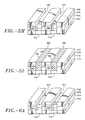
FIGS. 5A, 5B and 5D - 5I are schematic cross-sectional side views illustrating an
embodiment of IC structures of the present invention at sequential stages.
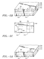
FIG. 5C shows a schematic plan view of the IC structure illustrated in FIG. 5B.
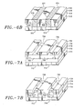
FIGS. 6A and 6B are schematic cross-sectional side views showing another
embodiment of IC structures illustrated in FIGS. 5A - 5I at sequential stages.
FIGS. 7A - 7C are schematic cross-sectional side views showing another
embodiment of IC structures illustrated in FIGS. 5A - 5I at sequential stages.
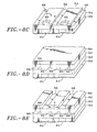
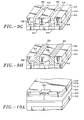
FIGS. 8A and 8C - 8G are schematic cross-sectional side views illustrating another
embodiment of IC structures of the present invention at sequential stages.
FIG. 8B shows a schematic plan view of the IC structure illustrated in FIG. 8A.
FIG. 8H shows a schematic plan view of the IC structure illustrated in FIG. 8G.
FIGS. 9A and 9C - 9H are schematic cross-sectional side views illustrating another
embodiment of IC structures of the present invention at sequential stages.
FIG. 9B shows a schematic plan view of the IC structure illustrated in FIG. 9A.
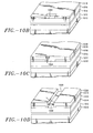
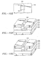
FIGS. 10A - 10D and 10F - 10K are schematic cross-sectional side views illustrating
another embodiment of IC structures of the present invention at sequential stages.
FIG. 10E shows a schematic plan view of the IC structure illustrated in FIG. 10D.
FIG. 11 is a block diagram illustrating a manufacturing system for fabricating the
IC structures of FIGS. 5A - 7C.
FIG. 12 is a block diagram illustrating a manufacturing system for fabricating the
IC structures exemplified in FIGS. 8A - 8H.
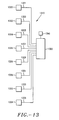
FIG. 13 is a block diagram illustrating a manufacturing system for fabricating the
IC structures of FIGS. 10A - 10K.
While describing the invention and its embodiments, certain terminology will be
utilized for the sake of clarity. It is intended that such terminology include not only the
recited embodiments but all equivalents which perform substantially the same function, in
substantially the same manner to achieve the same result.
In one embodiment of the invention, a novel dual damascene process is employed
wherein a rectangular via pattern is utilized in order to form misalignment tolerant dual
damascene structures. The expression "dual damascene structure" as defined herein,
includes an interconnect line in a trench and an underlying via plug which are formed
simultaneously. This process is illustrated in fabricated structures, such as the IC structures
shown in FIGS. 5A - 5I. The expression "integrated circuit structure" as defined herein,
includes completely formed integrated circuits and partially formed integrated circuits. FIG.
5A shows a structure generally similar to the prior art structure shown in FIG. 3A. A first
dielectric layer 516 is deposited on a semiconductor substrate 510 including interconnect
lines 512 and 514. The expression "semiconductor substrate" as defined herein, includes
structures and devices comprising typical integrated circuit elements, components,
interconnects and semiconductor materials. A second dielectric layer 518, having a
thickness typically ranging from about 50 Å to about 4000 Å, is deposited on first dielectric
layer 516. The first and second dielectric layers 516 and 518 have dissimilar etching
characteristics. The expression "dissimilar etching characteristics" of two materials as
defined herein, includes etching properties of these materials such that one of the materials
has a higher etch rate than the other material in a specific etch chemistry. A mask layer 520
is deposited on second dielectric layer 518.
As depicted in FIGS. 5B and 5C, mask layer 520 is developed to form novel
rectangular via patterns 522 and 524. These via patterns are shaped such that the length of
the via pattern is similar to the width of the overlaying trench pattern which will be formed
in a subsequent mask layer, such as width P of trench pattern 534 shown in FIG. 5F. The
length of the via pattern as used herein refers to the via pattern dimension which is
substantially parallel to the length of the trench pattern. For example, via pattern side 523
(FIG. 5C) forms the length dimension of via pattern 522. The width of the novel via
patterns exceeds the width of the overlaying trench pattern, preferably by at least 0.02µ,
wherein the via pattern width as used herein refers to the via pattern dimension which is
substantially perpendicular to the trench pattern. For example, via pattern side 525 (FIG.
5C) forms width dimension T of via pattern 522. FIGS. 5B and 5C show via pattern aligned
with substrate interconnect line 512, while via pattern 524 is misaligned with substrate line
514.
Via patterns 522 and 524 are anisotropically etched through second dielectric layer
518, forming via patterns 526 and 528 in layer 518, after which mask layer 520 is removed,
see FIG. 5D. In a subsequent processing step, shown in FIG. 5E, a third dielectric layer 530
is deposited on second dielectric layer 518 and inside via patterns 526 and 528 of layer 518.
Second and third dielectric layers 518 and 530 respectively have dissimilar etching
characteristics. Preferably, first and third dielectric layers 516 and 530 have similar etching
characteristics. The expression "similar etching characteristics" of two or more materials
as defined herein, includes etching properties of these materials such that the materials are
capable of being etched at similar etching rates in a particular etch chemistry. A second
mask layer 532 is deposited on dielectric layer 530. The dielectric and mask layers
described in connection with FIGS. 5A - 5E, can be deposited by any of the methods which
are well known to those of ordinary skill in the art.
As depicted in FIG. 5F, mask layer 532 is developed to form trench patterns 534 and
536 which are aligned with substrate lines 512 and 514 respectively. These trench patterns,
having a width P, provide the etch masks for dual damascene interconnect line trenches.
Trench patterns 534 and 536 are anisotropically etched through third dielectric layer 530
wherein second dielectric layer 518 is the etch stop, as shown in FIG. 5G. forming trenches
538 and 540 respectively. This anisotropic etching step also removes third dielectric layer
material which is present in those portions of via patterns 526 and 542 which are contained
within the trench patterns. When the via pattern is aligned with the corresponding trench.
such as via pattern 526 (FIG. 5G) the via pattern is opened across the entire width of the
trench. When the via pattern is misaligned, such as pattern 528, it may not be possible to
open the via pattern across the entire width of the trench depending on the width of the via
pattern and the extent of the misalignment. The structures illustrated in FIGS. 5F and 5G
show that the misalignment of via pattern 528 results in the formation of a reduced via
pattern 542. It is noted that width P of trench pattern 534 is measured at a point close to the
position of underlying via pattern 526.
Anisotropic etching is utilized to etch the via patterns through first dielectric layer
516, forming via holes 548 and 550 as depicted in FIG. 5G. The anisotropic via hole etching
process can be a continuation of the anisotropic trench etching process where layers 516 and
530 comprise the same material or where these layers have similar etching characteristics,
provided that second dielectric layer 518 is an etch stop in this process. The etch chemistry
for etching the via holes needs to be different from the etch chemistry for etching the
trenches if first and third dielectric layers 516 and 530 have dissimilar etching
characteristics.
Mask layer 532 is then removed, providing the structure shown in FIG. 5H which
includes trenches 538 and 540 extending through layer 530, and via holes 548 and 550
extending through layers 516 and 518. The trenches and via holes are simultaneously filled
with a conductive material such as a metal, creating novel dual damascene structures 552
and 554 (FIG. 51) including interconnect lines 556 and 558, and via plugs 560 and 562
respectively. Excess conductive material is removed from the surface of layer 530, for
example by planarizing using CMP (chemical-mechanical polishing) or by etch-back, using
any of the methods which are well known to those of ordinary skill in the art. FIGS. 5H and
5I show that misalignment of the novel rectangular via pattern results in a via hole and a via
plug having a reduced width compared with the width of the corresponding trench and
interconnect lines. However, the inventive rectangular via pattern results in less via width
reduction due to misalignment, than a conventional square via pattern. The inventive
technique utilizing the novel via patterns provides complete or partial compensation for
misalignment between etch masks, depending on the width of the novel via pattern and the
extent of the misalignment, thereby forming novel misalignment tolerant dual damascene
structures. The rectangular via pattern eliminates via width reduction which is caused by
misalignment, when the width of rectangular pattern equals (not shown) or exceeds (not
shown) the extent of the misalignment. It will be noted that novel via hole 550 (FIG. 5H)
provides complete or partial misalignment without widening trench 540, because the novel
via holes can only be formed within the trench pattern, This technique is therefore suitable
even if the via pattern width extends to half the distance between adjacent trench patterns.
Consequently, novel via plug 562 (FIG. 5I) provides complete or partial misalignment
compensation of dual damascene structures without widening interconnect line 558, thereby
preventing electrical shorts between adjacent interconnect lines.
An alternate embodiment of the inventive technique described in connection with
FIG. 5A - 5I is illustrated in fabricated structures shown in FIGS. 6A and 6B. In this
technique, the trenches are anisotropically etched through the third dielectric layer, similar
to the technique shown in FIG. 5H. This is followed by anisotropic etching of the trenches
through second dielectric layer 518, as shown in FIG. 6A, forming trenches 610 and 612
extending through layers 518 and 530. Via holes 614 and 616 of this structure extend
through layer 516. The present technique is advantageously employed if a cap or passivation
layer (not shown) is interposed between the substrate and the first dielectric layer. Where
a cap layer is employed, the anisotropic etching process for etching the trenches through
layer 518 can also be used to simultaneously etch the via holes through the cap layer,
providing the cap layer and layer 518 have similar etching characteristics. The trenches and
via holes can be simultaneously filled with a conductive material resulting in dual
damascene structures 618 and 620 shown in FIG. 6B, having interconnect lines 622 and 624
and via plugs 626 and 628. The advantages of the inventive techniques described in
connection with FIGS. 6A and 6B are similar to those described in connection with FIGS.
5A - 5I. Additionally, absence of dielectric layer 518 under lines 622 and 624 result in a
reduced capacitance of the structure as compared with structures having this layer
underneath the interconnect lines. The dielectric, cap and mask layers described in
connection with FIGS. 6A and 6B, can be deposited by any of the methods which are well
known to those of ordinary skill in the art.
The misalignment tolerant features of the present invention are further illustrated in
FIGS. 7A - 7C. The structure shown in FIG. 7A includes a substrate layer 710 having
interconnect lines 712 and 714, a first dielectric layer 716, a second dielectric layer 718
having novel rectangular via patterns 726 and 728, a third dielectric layer 730 and a mask
layer 732 having trench patterns 734 and 736. The materials and processes for fabricating
the structure shown in FIG. 7A are similar to those of the structure depicted in FIG. 5F.
Trench 734 (FIG. 7A) and novel via pattern 726 are aligned with interconnect line 712.
Trench 736 is misaligned with interconnect line 714 while novel via pattern 728 is aligned
with this interconnect line. By comparison, trench 536 show in FIG. 5F is aligned with
interconnect line 514. while the corresponding novel via pattern 528 is misaligned with line
514. The dimensions of via patterns 726 and 728 are similar to those of via patterns 526 and
528, i.e. the width of each via pattern exceeds the width of the overlaying trench by at least
0.02µ. Trenches 738 and 740 (FIG. 7B), and via holes 742 and 744 are formed in the
structure using techniques similar to those described in connection with FIGS. 5G and 5H.
The trenches and via holes are simultaneously filled with a conductive material, such as a
metal, forming novel dual damascene structures 746 and 748 (FIG. 7C) including
interconnect lines 750 and 752, and via plugs 754 and 756. The inventive technique
employing the novel via patterns provides complete or partial compensation for the
misalignment depending on the width of the novel via pattern and the extent of the
misalignment similar to the misalignment tolerance described in connection with FIGS. 5A -
6B.
An alternate embodiment of the present invention is illustrated in fabricated
structures, such as the IC structures shown in FIGS. 8A - 8H. The structure shown in FIG.
8A includes substrate 810 having interconnect lines 812 and 814, first and second dielectric
layers 816 and 818 and first mask layer 820. These layers and interconnect lines are similar
to those described in connection with FIG. 5A. Mask layer 820 is developed for square via
patterns 822 and 824 (FIG. 8A) which are similar to prior art via patterns, such as via
patterns 322 and 324 described in connection with FIGS. 3B and 3C. As depicted in FIGS.
8A and 8B, via pattern 822 is aligned with underlying substrate interconnect line 812, while
square via pattern 824 is misaligned with substrate line 814. Simultaneously with the
formation of the via patterns, mask layer 820 is developed for sacrificial etch patterns 826,
828 and 830. The expression "sacrificial etch pattern" as defined herein, includes one or
more etch patterns which are used to form one or more sacrificial etch segments in an etch
stop layer between adjacent dual damascene interconnect lines, as will be described more
fully in connection with FIGS. 8C - 8H. Sacrificial etch pattern 828 has a width W, as
shown in FIGS. 8A and 8B. Advantageously, the novel techniques employed in the present
embodiment provide for etch masks wherein the mask design includes the via patterns and
the sacrificial etch patterns. These techniques prevent misalignment between via patterns
and sacrificial etch patterns.
As depicted in FIG. 8C, the via patterns and the sacrificial etch patterns are
transferred to second dielectric layer 818, forming via patterns 832 and 834, and novel
sacrificial etch segments 836, 838 and 840, after which etch mask layer 820 is removed. Via
pattern 832 is aligned with underlying line 812, while via pattern 834 is misaligned with
underlying line 814. A third dielectric layer 842 is deposited on the remaining segments of
layer 818, see FIG. 8D. The deposition of layer 842 also fills via patterns 832 and 834, and
sacrificial etch segments 836, 838 and 840 with layer 842 material. A second mask layer 844
is deposited on layer 842. Trench patterns 846 and 848 (FIG. 8E) are formed in mask layer
844 to provide the etch masks for dual damascene interconnect line trenches, wherein D is
the distance between these trench patterns as measured near via patterns 832 and 834. These
trench patterns overlay the respective via patterns and the remaining segments of layer 818.
In other words, the trench patterns do not overlay the sacrificial etch segments. Trench
patterns 846 and 848 are employed to anisotropically etch trenches 550 and 552, and to
subsequently anisotropically etch via holes 554 and 556, after which mask layer 844 is
removed, see FIG. 8F. This etching process is similar to the techniques which are described
in connection with FIGS. 5G and 5H. The via holes and trenches are simultaneously filled
with a conductive material, such as a metal, thereby fabricating dual damascene structures
860 and 862, as shown in FIG. 8G. These structures include interconnect lines 864 and 866,
and via plugs 868 and 870 respectively. The dielectric and mask layers described in
connection with FIGS. 8A - 8H, can be deposited by any of the methods which are well
known to those of ordinary skill in the art.
As illustrated in FIGS. 8G and 8H, novel sacrificial etch segments 836, 838 and 840
provide gaps in etch stop layer 818 between the interconnect lines of the dual damascene
structures, resulting in a reduced capacitance between the dual damascene structures.
Alternatively, etch stop layer 818 can be removed (not shown) from trenches 850 and 852
(FIG. 8F), using techniques similar to those described in connection with FIGS. 6A and 6B.
This latter technique is suitable for forming dual damascene structures (not shown) having
sacrificial etch segments in the etch stop layer between the dual damascene interconnect
lines and having no etch stop layer underneath the lines, resulting in a further reduction in
the capacitance between the dual damascene structures of the present invention.
Layer 818 is an etch stop for the etching process which is used to form trenches 850
and 852 (FIG. 8F). Consequently, sacrificial etch segments 836, 838 and 840 should be
positioned such that the trench patterns overlay layer 818 rather than these sacrificial
segments. On the other hand, the sacrificial etch segments should form the widest possible
gaps between adjacent trench patterns in order to provide the greatest reduction in
capacitance between the resulting dual damascene structures. Proper positioning ofthe novel
sacrificial etch patterns relative to the trench pattens is further complicated by the possible
occurrence of etch mask pattern misalignments. It is well known to those of ordinary skill
in the art that pattern misalignments occur from time to time in the fabrication of IC
structures. Preferably, misalignment tolerant techniques should be utilized to compensate
for these misalignments by providing a sacrificial etch pattern wherein the pattern width is
smaller than the distance between the corresponding metal lines. For example, with
reference to FIGS. 8A, 8B and 8E, width W of sacrificial etch pattern 828 is preferably
smaller than distance D between trench patterns 846 and 848 in order to provide a
misalignment tolerant sacrificial etch pattern. It is noted that the width of a sacrificial etch
segment is similar to the width of the corresponding sacrificial etch pattern and that the
distance between adjacent dual damascene line trenches of the present invention is similar
to the distance between the corresponding trench patterns. Preferably, D exceeds W by a
measure which equals or exceeds the extent of the misalignment. Typically D exceeds W
by at least 0.02µ. Commonly used manufacturing and quality assurance methods can, for
example, be utilized to determine the size and statistical frequency of these misalignments
for any specific fabrication process.
In summary, the embodiment of the present invention described in connection with
FIGS. 8A - 8H is illustrative of the novel technique wherein one or more sacrificial etch
segments are provided in an etch stop layer between adjacent dual damascene structures, in
order to reduce the capacitance typically resulting from the presence of etch stop layer
material. This inventive technique includes forming one or more sacrificial etch segments,
such as sacrificial etch segment 828 (FIGS. 8A and 8B), in a dielectric stack. Trenches are
formed in the stack on the dielectric layer, such that the sacrificial etch segment is
positioned between the trenches. A via hole is formed underneath each trench. The via holes
communicate with their respective trenches and can for example, communicate with an
underlying substrate. Distance D between two adjacent trenches, preferable exceeds width
W of the sacrificial etch segment in order to compensate for possible misalignment between
etch mask patterns. More preferably, D exceeds W by a measure M of at least 0.02µ. The
trenches and via holes are simultaneously filled with a conductive material, such as a metal,
to form adjacent dual damascene structures having a gap in the etch stop layer between the
structures. Alternatively, the trenches can additionally be etched through the etch stop layer.
Another embodiment of the present invention, illustrated in FIGS. 9A - 9H,
combines the novel rectangular via patterns shown in FIGS. 5B - 7C with the novel
sacrificial etch patterns and novel sacrificial etch segments depicted in FIGS. 8A - 8H. The
structure illustrated in FIG. 9A includes a substrate 910 having substrate interconnect lines
912 and 914, a first dielectric layer 916, a second dielectric layer 918 and a first mask layer
920. The substrate, dielectric and mask layers are similar to those depicted in FIG. 5A. Mask
layer 922 is developed to form novel rectangular via patterns 922 and 924, similar to via
patterns 522 and 524 shown in FIGS. 5B and 5C. Via pattern 922 is aligned with line 912,
while via pattern 924 is misaligned with line 914. Simultaneously, first mask layer 920 is
developed to form novel sacrificial etch patterns 926, 928 and 930, similar to those
described in connection with FIGS. 8A and 8B.
As shown in FIG. 9C, via patterns 922 and 924, and sacrificial etch patterns 926, 928
and 930 are transferred to second dielectric layer 918 through anisotropic etching similar to
the techniques employed for fabricating the structures shown in FIGS. 5D and 8C. This
etching process forms via patterns 932 and 934 as well as sacrificial etch segments 936, 938
and 940. Subsequently, mask layer 920 is removed, as depicted in FIG. 9C. A third dielectric
layer 942 (FIG. 9D) is then deposited on layer 916 and in via patterns and sacrificial etch
segments 932, 934, 936, 938 and 940 respectively. Trench patterns 946 and 948 for dual
damascene interconnect line trenches are formed in a second etch mask layer 944 deposited
on layer 942, as depicted in FIG. 9E. Trench 946 is aligned with underlying substrate
interconnect line 912, while trench 948 is aligned with underlying line 914. Trench patterns
946 and 948 are anisotropically etched through dielectric layer 942 forming trenches 950
and 952 respectively, see FIG. 9F. The remaining segments of second dielectric layer 918
form an etch stop for the trench etching process. Via holes 954 and 956 are anisotropically
etched, after etching the trenches as described in connection with FIG. 5G. Mask layer 944
is removed, as shown in FIG. 9G. Via holes 954 and 956, and trenches 950 and 952 are
simultaneously filled with a conductive material, such as a metal, forming dual damascene
structures 954 and 956 (FIG. 9H) having interconnect lines 958 and 960, and via plugs 962
and 964 respectively. Preferably, the distance between the trench patterns exceeds the width
of sacrificial etch pattern as described in connection with FIGS. 8A - 8H, in order to provide
misalignment tolerant sacrificial etch segments.
Novel via hole 956 (FIG. 9G) and novel via plug 964 (FIG. 9H) provide
misalignment tolerant features similar to those described in connection with novel via hole
550 (FIG. 5H) and via plug 562 (FIG. 5I). Also, novel sacrificial etch segments 936, 938 and
940 (FIGS. 9G and 9H) provide similar capacitance reduction as previously described in
connection with novel sacrificial etch segments 836, 838 and 840 (FIGS. 8G and 8H). The
novel technique described in connection with FIGS. 9A- 9H thus combines the advantages
of the novel rectangular via patterns described in connection with FIGS. 5A - 7C with the
advantages of providing sacrificial etch segments as described in connection with FIGS. 8A
- 8H. The dielectric and mask layers described in connection with FIGS. 9A - 9H, can be
deposited by any of the methods which are well known to those of ordinary skill in the art.
Advantageously, the inventive techniques for forming novel sacrificial etch segments
employ only two etch masks. A first etch mask which is designed to include the via patterns
and the sacrificial etch patterns, while a second mask provides the trench patterns for etching
the dual damascene line trenches. The utilization of only two etch masks minimizes
fabrication cost and pattern misalignments. The inventive techniques which are described
in connection with FIGS. 5A - 9H utilize photoresist masks. However, it will be understood
that the invention is equally operable when hard masks or combinations of photoresist
masks and hard masks are used providing that the mask material has a low etch rate for the
etching procedures used in etching the dielectric layers of the inventive structures.
While the via holes and via plugs of the present invention illustrated in FIGS. 5A -
9H have typically been described and illustrated as making contact with a substrate
interconnect line, the invention is equally operable when the via holes and via plugs make
contact with one or more contact elements. A contact element as defined herein includes a
conductive component with provides a low resistivity contact between the via plug of a dual
damascene structure and circuit elements, interconnects or semiconductor material of a
structure, such as an IC structure.
The embodiments illustrated in FIGS. 5A - 9H are suitable for employing a variety
of dielectric stacks, providing that the etching characteristics of the materials meet the
criteria which are described in connection with these embodiments. Examples of suitable
dielectric stack materials for the second dielectric layer include oxides such as PECVD
(plasma-enhanced chemical vapor deposition) SiO2 and F-SiO2, nitrides such as CVD
(chemical vapor deposition) silicon nitride and silicon carbide, while suitable dielectric
materials for the first and third dielectric layers include materials having a low dielectric
constant, such as polymers, for example amorphous fluorinated carbon based materials,
spin-on dielectric polymers such as fluorinated and non-fluorinated poly(arylene) ethers
(commercially known as FLARE 1.0 and 2.0, which are available from Allied Signal
Company), poly(arylene) ethers (commercially known as PAE 2-3, available from
Schumacher Company), divinyl siloxane benzocyclobutane (DVS-BCB) or similar products
and aero-gel. These dielectric materials are well known to those of ordinary skill in the art.
The oxides, nitrides or carbides and the polymers have dissimilar etching characteristics
because the etch chemistries used for polymer etching, such as O2-based etch chemistries,
are highly selective with respect to SiO2, nitride or carbide. On the other hand, CHFx-based
chemistry typically used for etching SiO2 nitride or carbide is highly selective with respect
to polymer.
Additionally, suitable dielectric stacks meeting the above described etch criteria
include stacks wherein the second dielectric layer comprises silicon carbide or silicon nitride
and wherein the first and third dielectric layers comprise Black Diamond™, available from
Applied Materials, Inc. and described in commonly assigned U.S. Pat. application Serial No.
09/114,682, filed on July 13, 1998. Silicon nitride or silicon carbide dielectric materials and
Black Diamond™ have dissimilar etching characteristics.
An additional embodiment of the present invention is illustrated in FIGS. 10A -
10K, showing fabricated structures, such as IC structures, adapted for the formation of novel
dual damascene structures. The structure shown in FIG. 10A utilizes a first dielectric layer
1012 which is deposited on a substrate, such as a semiconductor substrate 1010. A second
dielectric layer 1014 is deposited on layer 1012. Subsequently, a third dielectric layer 1016
is deposited on layer 1014, followed by the deposition of a hard mask layer 1018. A first
photoresist layer 1020 is deposited on hard mask layer 1018. First and third dielectric layers
1012 and 1016 have similar etching characteristics while second and third dielectric layers
1014 and 1016 have dissimilar etching characteristics. Also, first and second dielectric
layers 1012 and 1014 have dissimilar etching characteristics. Second dielectric layer 1014
and hard mask layer 1018 have similar etching characteristics. The dielectric, hard mask and
photoresist layers of the structure depicted in FIG. 10A can be deposited by any of the
methods which are well known to those of ordinary skill in the art.
As shown in FIG. 10A, a novel rectangular via pattern 1022 is developed in resist
1020. The configuration is similar to the configuration of via patterns 522 and 524,
described in connection with FIGS. 5B and 5C, i.e. the width of via pattern 1022 exceeds
the width of the overlaying trench pattern, preferably by at least 0.02µ. Width X of via
pattern 1022 (FIG. 10A) is defined in a similar manner as width T of via pattern 522 (FIG.
5C), while width Y of trench pattern 1028 (FIG. 10D) is comparable to width P of trench
pattern 534 (FIG. 5F). In other words, width X (FIG. 10A) of via pattern 1022 is greater than
width Y of trench pattern 1028 (FIG. 10D), while the length of the via pattern is similar to
the width of the trench pattern. Via pattern 1022 is transferred to hard mask layer 1018
through anisotropic etching, forming via pattern 1024 in layer 1018, after which first resist
layer 1020 is stripped, see FIG. 10B. A second photoresist layer 1026 (FIG. 10C) is
deposited on hard mask layer 1018 and inside via pattern 1024. Second resist layer 1026 is
developed for a trench pattern 1028 (FIGS. 10D and 10E) for the fabrication of a dual
damascene line trench, This process also results in removing resist 1026 from the portion
of via pattern 1024 underlying trench pattern 1028, thereby forming via pattern 1030 (FIG.
10D). Via pattern 1030 is anisotropically etched through layer 1016, see FIG. 10F, wherein
second dielectric layer 1014 is an etch stop. Next, trench pattern 1028 is anisotropically
etched through hard mask layer 1018, while simultaneously anisotropically etching via
pattern 1030 through second dielectric layer 1014, as depicted in FIG. 10G.
French pattern 1028 and via pattern 1030 are simultaneously anisotropically etched
through dielectric layers 1016 and 1012 (FIG. 10H) forming trench 1032 and via hole 1034
respectively. Trench 1032 extends through layer 1016, while via hole 1034 extends through
layers 1012 and 1014 to substrate 1010. Next, resist 1026 is stripped, see FIG. 101. This is
followed by the removal of hard mask layer 1018 (FIG. 10J). As shown in FIG. 10K, trench
1032 and via hole 1034 are simultaneously filled with a conductive material, such as a
metal, forming novel dual damascene structure 1036 including interconnect line 1038 and
via plug 1040. The novel technique of the present embodiment illustrated in FIGS. 10A -
10K, provides novel rectangular via patterns which compensate partly or completely for
misalignment between the via pattern and the trench pattern without causing any widening
of the line trench and the interconnect line, because the via holes can only be formed within
the trench pattern. This technique is therefore suitable even if the via pattern width extends
to half the distance between adjacent trench patterns. Consequently, the via patterns of the
present invention result in via plugs which do not cause an electrical short between closely
spaced interconnect lines of dual damascene structures. Also, these via patterns can be
fabricated such that the length of the via pattern does not exceed the width of the
corresponding dual damascene trench pattern thus resulting in via plugs having a cross
sectional length dimension which does not exceed the width of the corresponding
interconnect line, thereby maximizing the number of via plugs which can be fabricated on
the corresponding interconnect line.
A variety of dielectric stacks can be utilized for the embodiment illustrated in FIGS.
10A - 10K, providing that the etching characteristics of the materials meet the criteria which
are described in connection with these embodiments. Examples of suitable dielectric stack
materials for the second dielectric layer and hard mask layer include oxides such as
PECVD SiO2 and F-SiO2 as well as silicon carbide, while suitable dielectric materials for
the first and third dielectric layers include materials having a low dielectric constant, such
as polymers, for example amorphous fluorinated carbon based materials, spin-on dielectric
polymers such as fluorinated and non-fluorinated poly(arylene) ethers (commercially known
as FLARE 1.0 and 2.0, which are available from Allied Signal Company), poly(arylene)
ethers (commercially known as PAE 2-3, available from Schumacher Company), divinyl
siloxane benzocyclobutane (DVS-BCB) or similar products and aero-gel. These dielectric
materials are well known to those of ordinary skill in the art. The oxides, nitrides or carbides
and the polymers have dissimilar etching characteristics because etch chemistries used for
polymer etching, such as O2-based etch chemistries, are highly selective with respect to
SiO2, nitride or carbide. On the other hand, CHFx-based chemistry typically used for etching
SiO2, nitride or carbide is highly selective with respect to polymer. Suitable dielectric
stacks also include stacks wherein the second dielectric layer and the hard mask layer
comprise silicon nitride or silicon carbide, while the first and third dielectric layers comprise
Black Diamond™. Another example of a suitable dielectric stack for the structures shown
in FIGS. 10A - 10K includes second dielectric layer and mask layer materials comprising
nitride, such as CVD (chemical vapor deposition) silicon nitride or silicon carbide, while
dielectric materials for first and third dielectric layers 712 and 716 include oxides, such as
PECVD SiO2 and F-SiO2.
Embodiments of the present invention illustrated in FIGS. 5A - 7C and 9A - 10K
have been described by means of rectangularly shaped via patterns. It will be understood that
the invention is also operable when other via shapes such as ellipse and oval are utilized,
provided that these shapes, at their widest points, exceed the width of the corresponding
damascene line trench. As is well known by those of ordinary skill in the art, a rectangular
etch pattern can result in an etched hole having rounded corners at the bottom,
approximating an ellipse or oval shape.
Additional embodiments (not shown) of the present invention include depositing a
liner inside the via holes and trenches of the IC structures shown in FIGS. 5H, 6A, 7B, 8F,
9G and 10J. The lined via holes and trenches are then simultaneously filled with a
conductive material to form the dual damascene structures of the present invention. Suitable
liner materials include adhesion promoters and diffusion barrier materials. For example
suitable liner materials for Cu or Cu alloy containing damascene structures of the present
invention include CVD or PVD (physical vapor deposition) TiN, WN, Ta and TaN.
Examples of suitable liner materials for Al. Al alloy, W, or W alloy containing damascene
structures include PVD Ti/TiN.
Suitable semiconductor materials for use in semiconductor substrates of the present
invention include silicon, germanium, silicon/germanium alloys, gallium arsenide and
indium/gallium/arsenide/phosphide. Typically, dual damascene structures of the present
invention contact a metallized line of the semiconductor substrate. Suitable conductive
materials for filling the damascene trenches and via holes of the present invention include
metals such as Cu, Ag. Al, W, their alloys and mixtures of these metals with or without
alloys. While the embodiments of the invention are described and illustrated using metal
interconnect lines and metal damascene structures, the invention is equally operable when
conductive materials other than metals are used. Suitable conductive materials include
metallic and nonmetallic superconductors, i.e. materials having zero direct current resistance
at or below their superconducting transition temperature, such as metallic nickel/germanium
and nonmetallic yttrium/barrier/copper oxides. Suitable techniques for simultaneously filling
damascene trenches and via holes include CVD, PVD, electroplating and electroless plating.
These techniques are well known to those of ordinary skill in the art. The various etching
techniques and etching chemistries employed in the embodiments of the present invention
include techniques and chemistries which are well known to those of ordinary skill in the
art. Also, it will be understood that it is necessary to clean or prepare the surface of the
structure prior to the deposition of any layer in any subsequent fabrication step, using
surface preparation methods and materials which are well known to those of ordinary skill
in the art. It will also be understood that methods for removing resist include conventional
dry and wet methods.
Embodiments of the present invention are illustrated herein using IC structures
containing one or two dual damascene structures. It will be understood that the inventive
techniques are equally operable for the fabrication of IC structures containing multiple dual
damascene structures throughout the IC structure.
The novel dual damascene fabrication techniques of the present invention require
a sequence of processing steps. Each processing step can be performed at a fabrication
station. All or some of the fabrication stations and their respective processing steps can be
integrated by means of a novel apparatus including a controller 1100 illustrated in FIG. 11.
Controller 1100 is adapted for controlling a number of fabrication stations which are utilized
in the formation of fabricated structures, such as the IC structures described in connection
with FIGS. 5A - 7C. As illustrated in FIG. 11, a novel manufacturing system 1110 for
fabricating IC structures includes controller 1100 and a plurality of fabrication stations:
1120, 1122, 1124, 1126, 1128, 1130 and 1132. Additionally, system 1110 has operative
links 1121, 1123, 1125, 1127, 1129, 1131 and 1133 which provide connections between
controller 1100 and fabrication stations 1120, 1122, 1124, 1126, 1128, 1130 and 1132
respectively. The novel apparatus includes a data structure such as a computer program
which causes controller 1100 to control the processing steps at each of the fabrication
stations and to, optionally, regulate the sequence in which fabrication stations are used in
order to form the novel structures.
Examples of suitable controllers include conventional computers and computer
systems including one or more computers which are operably connected to other computers
or to a network of computers or data processing devices. Suitable computers include
computers commonly known as personal computers. The data structure which is used by
controller 1100 can be stored on a removable electronic data storage medium 1140 (FIG.
11), such as computer floppy disks, removable computer hard disks, magnetic tapes and
optical disks, to facilitate the use of the same data structure at different manufacturing
locations. Alternatively, the data structure can be stored on a non-removable electronic data
storage medium, including a medium positioned at a location which is remote (not shown)
from
controller 1100, using such data storage devices as are well known to those or ordinary
skill in the art. The data structure can be communicated from a remote location to
controller
1100 using communicating techniques which are well known to those of ordinary skill in
the art including hard wire connections, wireless connections and data communication
methods utilizing one or more modems or techniques using one or more computers
commonly known as servers. The data storage medium can be operably connected to the
controller using methods and device components which are well know to those of ordinary
skill in the art. Examples of suitable fabrication stations for
manufacturing system 1110
include the stations shown in Table A.
| Station | Processing Stop | |
| 1120 | depositing a first dielectric layer on a substrate |
| 1122 | depositing a second dielectric layer on the first dielectric layer |
| 1124 | depositing a first mask layer having a via pattern on the second dielectric layer |
| 1126 | anisotropically etching the via pattern through the second dielectric layer |
| 1128 | removing the first mask layer |
| 1130 | depositing a third dielectric layer on the second dielectric layer |
| 1132 | depositing a second etch mask having a trench pattern overlaying the via pattern on the third dielectric layer |
Additional fabrication stations can be added to manufacturing system 1110. The
sequence of processing steps shown in Table A is illustrative of system 1110. However, the
invention is equally operable in systems wherein a controller, such as controller 1100,
causes the sequence to be altered, for example by repeating a previously executed
processing step if test results indicate that this processing step should be partly or
completely repeated. Alternatively, the process sequence which is controlled by a controller
such as controller 1100, can include processing steps such as surface preparation which may
be performed following any of the fabrication stations shown in FIG. 11 and Table A. It is
also contemplated that one or more fabrication stations can be positioned at a location which
is remote from the other fabrication stations in which case an additional controller or a
network of controllers can be employed to control the remotely located manufacturing
station. As illustrated in FIG. 11, controller 1100 is adapted to be connected to each of the
manufacturing stations through operative links. Each of these links provides a bidirectional
connection enabling controller 1100 to transfer commands from its data structure, such as
specific operating parameters, and to receive information, such as test data, from the
fabrication station. The operative links can be in the form of hard wire connections or
wireless connections.
FIG. 12 depicts another embodiment of the present invention. A novel apparatus
including
inventive controller 1200 is adapted for controlling fabrication stations which are
utilized in the formation of fabricated structures, such as IC structures described in
connection with FIGS. 8A - 8H.
Fabrication stations 1220, 1222, 1224, 1226, 1228 and
1230 are connected to
controller 1200 through
operative links 1221, 1223, 1225, 1227, 1229
and 1231 respectively. The novel apparatus includes a data structure which causes the
controller to control the processing steps at each of the fabrication stations. A
novel
manufacturing system 1210 for manufacturing the structures exemplified in FIGS. 8A- 8H
includes
controller 1200, the data structure, the above manufacturing stations and the
operative links. The data structure can be provided on a removable
electronic storage
medium 1240. The controller, the data structure, the operative links and the removable
storage medium are similar to those described in connection with FIG. 11. Examples of
suitable fabrication stations for
manufacturing system 1210 include the stations shown in
Table B.
| Station | Processing Step | |
| 1220 | forming a dielectric stack including an etch stop layer |
| 1222 | forming a sacrificial etch segment in the etch stop layer |
| 1224 | forming a first trench on the etch stop layer |
| 1226 | forming a second trench on the etch stop layer |
| 1228 | forming a first via hole underlying the first trench |
| 1230 | forming a second via hole underlying the second trench |
FIG. 13 depicts another embodiment of the present invention. A novel apparatus
including
inventive controller 1300 is adapted for controlling fabrication stations which are
utilized in the formation of fabricated structures, such as IC structures described in
connection with FIGS. 10A - 10K.
Fabrication stations 1320, 1322, 1324, 1326, 1328, 1330,
1332 and 1334 are connected to
controller 1300 through
operative links 1321, 1323, 1325,
1327, 1329, 1331, 1333 and 1335 respectively. The novel apparatus includes a data structure
which causes the controller to control the processing steps at each of the fabrication stations.
A
novel manufacturing system 1310 for manufacturing the structures illustrated in FIGS.
10A - 10K includes
controller 1300, the data structure, the above manufacturing stations and
the operative links. The data structure can be provided on a removable
electronic storage
medium 1340. The controller, the data structure, the operative links and the removable
storage medium are similar to those described in connection with FIG. 11. Examples of
suitable fabrication stations for
manufacturing system 1310 include the stations shown in
Table C.
| Station | Processing Step | |
| 1320 | depositing a first dielectric layer on a substrate |
| 1322 | depositing a second dielectric layer on the first dielectric layer |
| 1324 | depositing a fluid dielectric layer on the second dielectric layer |
| 1326 | depositing a hard mask layer on the third dielectric layer |
| 1328 | depositing a first photoresist layer having a via pattern on the hard mask layer |
| 1330 | anisotropically etching the via pattern through the hard mask layer |
| 1332 | removing the first photoresist layer |
| 1334 | depositing a second photoresist having a trench pattern overlaying the via pattern on the hard mask layer |
The invention has been described in terms of the preferred embodiment. A person
of ordinary skill in the art will recognize that it would be possible to construct the elements
of the present invention from a variety of means and to modify the placement of components
in a variety of ways. While the embodiments of the invention have been described in detail
and shown in the accompanying drawings, it will be evident that various further
modifications are possible without departing from the scope of the invention as set forth in
the following claims.