EP1027641B1 - Computer-prozessor und verfahren zum kontinuierlichen schreiben und lesen von daten - Google Patents
Computer-prozessor und verfahren zum kontinuierlichen schreiben und lesen von daten Download PDFInfo
- Publication number
- EP1027641B1 EP1027641B1 EP98956631A EP98956631A EP1027641B1 EP 1027641 B1 EP1027641 B1 EP 1027641B1 EP 98956631 A EP98956631 A EP 98956631A EP 98956631 A EP98956631 A EP 98956631A EP 1027641 B1 EP1027641 B1 EP 1027641B1
- Authority
- EP
- European Patent Office
- Prior art keywords
- register
- operand
- address
- registers
- register file
- Prior art date
- Legal status (The legal status is an assumption and is not a legal conclusion. Google has not performed a legal analysis and makes no representation as to the accuracy of the status listed.)
- Expired - Lifetime
Links
Images


Classifications
-
- G—PHYSICS
- G06—COMPUTING OR CALCULATING; COUNTING
- G06F—ELECTRIC DIGITAL DATA PROCESSING
- G06F9/00—Arrangements for program control, e.g. control units
- G06F9/06—Arrangements for program control, e.g. control units using stored programs, i.e. using an internal store of processing equipment to receive or retain programs
- G06F9/30—Arrangements for executing machine instructions, e.g. instruction decode
- G06F9/30003—Arrangements for executing specific machine instructions
- G06F9/30007—Arrangements for executing specific machine instructions to perform operations on data operands
- G06F9/3001—Arithmetic instructions
-
- G—PHYSICS
- G06—COMPUTING OR CALCULATING; COUNTING
- G06F—ELECTRIC DIGITAL DATA PROCESSING
- G06F9/00—Arrangements for program control, e.g. control units
- G06F9/06—Arrangements for program control, e.g. control units using stored programs, i.e. using an internal store of processing equipment to receive or retain programs
- G06F9/30—Arrangements for executing machine instructions, e.g. instruction decode
- G06F9/30098—Register arrangements
- G06F9/3012—Organisation of register space, e.g. banked or distributed register file
- G06F9/3013—Organisation of register space, e.g. banked or distributed register file according to data content, e.g. floating-point registers, address registers
-
- G—PHYSICS
- G06—COMPUTING OR CALCULATING; COUNTING
- G06F—ELECTRIC DIGITAL DATA PROCESSING
- G06F9/00—Arrangements for program control, e.g. control units
- G06F9/06—Arrangements for program control, e.g. control units using stored programs, i.e. using an internal store of processing equipment to receive or retain programs
- G06F9/30—Arrangements for executing machine instructions, e.g. instruction decode
- G06F9/34—Addressing or accessing the instruction operand or the result ; Formation of operand address; Addressing modes
- G06F9/345—Addressing or accessing the instruction operand or the result ; Formation of operand address; Addressing modes of multiple operands or results
-
- G—PHYSICS
- G06—COMPUTING OR CALCULATING; COUNTING
- G06F—ELECTRIC DIGITAL DATA PROCESSING
- G06F9/00—Arrangements for program control, e.g. control units
- G06F9/06—Arrangements for program control, e.g. control units using stored programs, i.e. using an internal store of processing equipment to receive or retain programs
- G06F9/30—Arrangements for executing machine instructions, e.g. instruction decode
- G06F9/38—Concurrent instruction execution, e.g. pipeline or look ahead
- G06F9/3885—Concurrent instruction execution, e.g. pipeline or look ahead using a plurality of independent parallel functional units
Definitions
- This invention pertains in general to microprocessors and in particular to a processor for performing media operations. More particularly, this invention pertains to a processor having a modified Harvard memory architecture and performing streaming ALU operations.
- DSP digital signal processing
- graphics processing graphics processing
- audio processing audio processing
- video processing video processing
- a typical algorithm will process a large number of elements while using each element only once.
- a typical DSP filter loop will process a large number of different input samples and apply a different operand from a large coefficient array to each input sample.
- a typical cycle of operation in such a processing environment requires 1) determining the addresses of the sample and coefficient; 2) retrieving the sample and coefficient from memory; 3) operating on the sample and coefficient; and 4) storing the result of the operation.
- RISC reduced instruction set computer
- a RISC architecture uses a low-complexity design adapted to handle a small set of simple instructions in order to obtain high-speed and high-performance.
- a RISC architecture uses fixed length instructions with very few instruction formats and fixed positions for certain operand fields, like register indices, within the instruction format. This architecture allows for low-complexity instruction decoders and control logic and this lower complexity can be leveraged into increased performance from other parts of the processor.
- ALU arithmetic logic unit
- CISC complex instruction set computer
- processors supporting superscalar instruction scheduling dynamically extract instruction-level parallelism from the instruction stream and then group loads and stores with ALU operations. In this manner, the instructions can utilize parallel functional units in the processor.
- processors are highly complex in terms of design and size.
- VLIW very long instruction word
- the VLIW format explicitly encodes instruction-level parallelism into a very long instruction word.
- the VLIW typically has fields for frequently performed operations, such as ALU operations and memory accesses.
- VLIW format essentially demands that parallelism in the instruction stream be determined when the program is compiled. This demand results in an extremely complex programming model and, accordingly, a difficult program compilation. Thus, the gains made in processing efficiency by using the VLIW format are offset by the compile-time difficulties.
- the processor preferably has a modified Harvard memory architecture with first and second addressable memories, an address register file having first and second groups of address register sets, first and second address generation units respectively coupled to the first and second groups of address register sets, first and second stream registers, a general purpose register (GPR) file, and an arithmetic logic unit (ALU).
- GPR general purpose register
- ALU arithmetic logic unit
- the address register file preferably includes eight register sets divided into two groups of four register sets each. Each register set contains a base register, a step register, and a modulo register.
- the first and second groups of address register sets respectively address the first and second addressable memories. When a memory access is made to an address register set, contents in that address register set are sent to the respective addressable memory as the address.
- the first and second address generation units respectively update the contents of selected address register sets in the first and second groups according to one of six addressing modes.
- the first and second addressable memories output data in response to receiving an address from an address register set. These data arc respectively stored in the first and second stream registers.
- the GPR register file contains 32 GPRs.
- the ALU accepts two operands as inputs, the first of which is either the first stream register or a GPR and the second of which is either the second stream register or a GPR.
- the ALU output may be stored in the first or second addressable memory or a GPR.
- a stream instruction encodes an operand selection field and three operand fields.
- the operand selection field selects the operands for the ALU operation and specifies whether to store the result in the first or second addressable memories or a GPR.
- the first and second operand fields specify operands for use by an ALU operation performed by a subsequent stream instruction.
- the first operand can specify either a register set in the first group in the address register file and an addressing mode or a GPR.
- the second operand can specify either a register set in the second group and an addressing mode or a GPR. Five bits are needed to choose either a register set and addressing mode or a particular GPR. Accordingly, the bits for addressing a GPR are positionally the same as the bits for selecting a register set and an addressing mode.
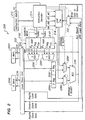
- FIG. 2 is high-level a block diagram illustrating certain functional components of a processor 200 constructed according to an embodiment of the present invention. Shown are an instruction memory 210, an instruction decoder 214, X and Y address register files 216, and a general purpose register (GPR) file 218. Also shown are X and Y address generation units (AGUs), a load/store unit 222, an X memory 224X, and a Y memory 224Y. In addition, FIG. 2 shows X and Y stream registers 226, X and Y multiplexers (MUXs) 228, an arithmetic logic unit (ALU) 230, and a GPR MUX 232.
- AGUs X and Y stream registers 226, X and Y multiplexers (MUXs) 228, an arithmetic logic unit (ALU) 230, and a GPR MUX 232.
- the instruction memory 210 is coupled to the instruction decoder 214 and holds instructions for the program being executed by the processor 200.
- the instruction memory 210 receives a program counter from the instruction decoder 214 that identifies an instruction in the memory 210. The identified instruction is transmitted from the instruction memory 210 to the instruction decoder 214.
- the instruction decoder 214 is coupled to the instruction memory 210, the X and Y address register files 216, and the GPR file 218. In addition, the instruction decoder 214 is coupled via control lines (shown as dashed lines in FIG. 2) to the X and Y address register files 216, the load/store unit 222, the X and Y MUXs 228, the ALU 230, and the GPR MUX 232.
- the instruction decoder decodes instructions received from the instruction memory 210 and controls the operation of the processor 200 in response thereto. For purposes of this discussion, assume that the received instruction is a streaming ALU instruction. As will be described in more detail below, the streaming ALU instruction specifies three operands: two sources and one destination.
- the source operands are selected from among the X and Y stream registers 226 and the GPR file 218.
- the destination operand is selected from either the X or Y memory 224 or the GPR file 218.
- the instruction decoder 214 While decoding the instruction, the instruction decoder 214 sends a first index from the first operand to the X address register file 216X, a second index from the second operand to the Y address register file 216Y, and all three operands to the GPR file 218.
- the instruction decoder 214 sends control signals to the AGUs 220 indicating address modes of the instruction and to the GPR file 218 indicating whether the GPR MUX 232 will write to the GPR file 218.
- the X and Y address register files 216 respectively receive the X and Y indices from the instruction decoder 214.
- the X and Y address register files 216 are each coupled to respective AGUs 220 and to the load/store unit 222.
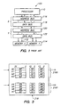
- FIG. 3 illustrates a more detailed view of the address register file 216.
- the address register file 216 has eight address register sets A0-A7 divided into two groups of four register sets each A0-A3, A4-A7. The first group of four register sets forms the X register file 216X while the second group of four register sets forms the Y register file 216Y.
- the X and Y AGUs 220 respectively receive the contents of the X and Y address registers and the address mode control signals from the instruction decoder 214 and have an output coupled to the inputs of the X and Y address register files 216.
- the AGUs 220 post-modify the selected base registers B0 according to the addressing mode and the step S0 and modulo M0 registers.
- Modes supported by the AGUs 220 include: 1) auto post decrement; 2) auto post increment; 3) step post decrement; 4) step post increment; 5) base (no modification); and 6) bit reversed.
- the base register B0 is modified according to the contents of a user processor status register (not shown). In modes three and four.
- the respective X and Y address register files 216 also send the contents of the selected base registers to the load/store unit 222.
- the load/store unit 222 is coupled to the X and Y address register files 216, the X and Y stream registers 226, the ALU 230, the GPR MUX 232, and the GPR file 218 and receives control signals from the instruction decoder 214.
- the load/store unit 222 is bi-directionally coupled to the X and Y memories 224.
- the couplings 223 between the load/store unit 222 and the memories 224 each comprise separate address and data busses like those shown in FIG. 1 and, thus, form a modified Harvard architecture.
- the X and Y 224 memories are coupled to the load/store unit 222 and are addressable memories. In response to receiving a memory address and control signals from the load/store unit 222, the memories either store an input at the referenced memory address or output the contents of the referenced memory address.
- the instruction decoder 214 When decoding a stream instruction, the instruction decoder 214 sends the three operand fields in the stream instruction to the GPR file 218.
- the first two operands specify the sources for the streaming ALU 230 operation. Since there are 32 GPRs in the file 218, five-bit indices in each of the first two operand fields specify particular GPRs in the GPR file 218.
- the contents of the GPR specified by the first operand are sent to the MUX 228X corresponding to the X register 226X and the contents of the GPR specified by the second operand are sent to the MUX 228Y corresponding to the Y register 226Y.
- the third operand along with the operand selection field described below, specifies the destination of the result of the ALU 230 operation. If this destination is a GPR, then the GPR file 218 receives the result from the ALU 230 via the GPR MUX 232 and stores it in the GPR identified by the third operand.
- the X and Y MUXs 228 respectively receive the contents of the X and Y stream registers 226 and the contents of the specified first and second GPRs.
- the outputs of the MUXs 228 are passed to the ALU 230.
- Each MUX receives control signals from the instruction decoder 214 specifying which input the MUX will output to the ALU 230.
- the ALU 230 receives inputs from the MUXs 228, receives control signals from the instruction decoder 214, and has an output coupled to the load/store unit 222 and the GPR MUX 232.
- the ALU 230 performs an arithmetic operation on its inputs and produces an output. The type of operation performed is specified by the control signals received from the instruction decoder 214.
- the GPR MUX 232 has an input coupled to the ALU 230 output and an input coupled to an output of the load/store unit 222, receives control signals from the instruction decoder 214, and has an output coupled to the GPR file 218. When so controlled by the instruction decoder 214, the GPR MUX 232 outputs a received input to the GPR file 218.
- FIG. 4 illustrates instruction encoding for a streaming ALU instruction of the type decoded by the instruction decoder 214.
- FIG. 4 there are eight instruction encoding formats and each instruction encoding format is identified by a three letter code that specifies the operands for that format. The three letters respectively specify the source of the first operand, the source of the second operand, and the destination for the results of the ALU 230 operation.
- the letter "X" specifies the X stream register 226X
- the letter "Y” specifies the Y stream register 226Y
- the letter "R" specifies a GPR.
- the instruction format 400 is preferably 32 bits in length. Bits 14-10, labeled “A,” identify the first operand, bits 9-5, labeled “B,” identify the second operand, and bits 20-16, labeled “C,” identify the third operand. Op6 bits 2-0, labeled as “D,” specify the type of encoding (operands) used by the instruction format. Op1-5 bits 27-21. 15, and 4-3, labeled as “E,” contain operation codes (opcodes) for the instruction format. Finally, COND bits 31-28, labeled as "F,” identify the conditions under which the instruction will execute.
- Field D is a three-bit operand select field that specifies from where the first and second operands of the ALU are read and to where the result of the ALU 230 operation is stored (operand 3).
- Table 1 indicates the possible operand combinations, the corresponding value of field D (Op6), and the corresponding reference numeral in FIG. 4.
- the first operand is selected from either a GPR or the X stream register 226X.
- the second operand in contrast, is selected from either a GPR or the Y stream register 226Y.
- the third operand can be stored in X memory 224X, Y memory 224Y, or a GPR.
- Fields A. B, and C respectively specify the first. second. and third operands.
- the first A and second B operands are used to update the inputs to the ALU 230 (the stream registers 226 and the GPR file 218) for use by a subsequent ALU 230 operation.
- the values specified by the first and second operands overwrite the values previously held in the stream registers 226.
- the third operand indicates where to store the result of the current ALU 230 operation.
- each of the operand fields A,B,C is five bits wide. Since there are only four register sets in each of the X and Y address register files 216. and since the first operand A can only select register sets in the X register file 216X and the second operand B can only select register sets in the Y register file 216Y, only two bits of encoding within the first A and second B operand fields are needed to select a particular register set within the address register file 216. In addition, three bits of encoding are needed to select among the possible addressing modes. Table 2 lists the possible addressing modes and the associated address mode bits.
- operand fields A,B,C the five bits used to select a GPR are overlapped with the two-bit subfield for the address register index and the three-bit subfield for the addressing mode.
- instruction format 410 is for an RRR instruction and, accordingly, all three operand are illustrated as five-bit fields A,B,C.
- Instruction format 418 is an RYX instruction and the five-bit fields for the second B and third C operands are shown as divided into three- and two-bit subfields.
- the programmer uses the five-bit operand field to specify the GPR.
- the programmer wants to use the X stream register 226X as the first operand.
- the programmer puts the two-bit index for the register set and three bits specifying the addressing mode in the first operand field A.
- the programmer can use the Y stream register 226Y as the second operand in the same manner. If the address mode bits are set to 000, then the value in the X or Y stream register 226 is used without initiating a memory fetch or updating the address register 216.
- the opfields E describe the computation to be performed by the processor.
- the COND field F describes conditions to be checked before the computation is performed.
- FIG. 5 is a timing chart illustrating the steps performed by the processor 200 when executing a stream instruction like those illustrated in FIG. 4.
- time flows in the direction indicated by the arrow 500 on the left of the figure and the boxes to the right illustrate the order in which the indicated steps are performed by functional units of the processor 200. Since the functional units of the processor 200 operate in parallel, FIG. 5 should not be construed to indicate that time-aligned steps occur at the same time, but rather merely indicates the approximate sequence in which steps are performed.
- a stream instruction like that illustrated in FIG. 4 is received by the instruction decoder 214 T0.
- the instruction decoder 214 sends the index bits of the first and second operands to the X and Y address register files 216, respectively.
- the instruction decoder 214 sends all three of the operands to the GPR file 218.
- the instruction decoder decodes the Op6 field to determine the operands to the current ALU 230 operation and where the result should he stored.
- the ALU 230 reads the selected inputs from the instruction decoder 214.
- the address register files 216 pass the contents of the selected registers to the load/store unit 222 and cause the appropriate values to be loaded into the X and Y stream registers 226. Also, the AGUs 220 update the address registers selected by the index bits. At the same time, the ALU 230 operation indicated by the decoded instruction is performed on the previously read operands.
- the data in the X streaming register 228X are added to the data in the Y streaming register 228Y by the ALU 230.
- the result of this add operation is stored in the identified GPR.
- a fetch is initiated from X memory 224X for the data addressed by [x] and is stored in the X streaming register 226X.
- a fetch is initiated from Y memory 224Y for the data addressed by [y] and is stored in the Y streaming register 226Y.
- the base registers of the [x] and [y] registers within the address register file 216 are updated.
Landscapes
- Engineering & Computer Science (AREA)
- Software Systems (AREA)
- Theoretical Computer Science (AREA)
- Physics & Mathematics (AREA)
- General Physics & Mathematics (AREA)
- General Engineering & Computer Science (AREA)
- Computational Mathematics (AREA)
- Mathematical Analysis (AREA)
- Mathematical Optimization (AREA)
- Pure & Applied Mathematics (AREA)
- Advance Control (AREA)
- Executing Machine-Instructions (AREA)
Claims (20)
- Verfahren zum Ausführen eines Befehls mit einem ersten, einem zweiten und einem dritten Operandenfeld (A, B, C), einem Operanden-Spezifikationsfeld (D), und zum Spezifizieren einer logischen Operation, mit folgenden Verfahrensschritten:Ausführen der spezifizierten logischen Operation mit einem ersten Wert, der ausgewählt wird aus einem ersten Register (226X) und einer Ausgabe einer ersten Allzweck-Registerdatei (218), und mit einem zweiten Wert, der ausgewählt wird aus einem zweiten Register (226Y) und einer Ausgabe einer zweiten Allzweck-Registerdatei (218), um ein Ergebnis zu erzeugen, wobei das Operanden-Spezifikationsfeld (D) spezifiziert, woher der erste und der zweite Wert ausgewählt werden sollen;Speichern des Ergebnisses der logischen Operation an einer Stelle, welche durch den dritten Operanden (C) und das Operanden-Spezifikationsfeld (D) identifiziert wird; Aktualisieren eines Wertes in dem ersten Register (226X) gestützt auf das erste Operandenfeld (A) und eine Adreßregisterdatei (216) vor einer nachfolgenden Operation; undAktualisieren eines Wertes in dem zweiten Register (226Y) gestützt auf das zweite Operandenfeld (B) und die Adreßregisterdatei (216) vor einer nachfolgenden Operation.
- Verfahren nach Anspruch 1, wobei der Schritt des Aktualisierens eines Wertes in dem ersten Register (226X) die folgenden Unterschritte umfaßt:Liefern eines ersten Index in dem ersten Operandenfeld (A) an die Adreßregisterdatei (216); undAuswählen eines ersten Adreßregisters (226) in der Adreßregisterdatei (216), welche eine Adresse entsprechend dem ersten Index enthält.
- Verfahren nach Anspruch 2, mit den weiteren Verfahrensschritten:Wiedergewinnen eines Wertes, der durch die Adresse spezifiziert wird, aus einem adressierbaren Speicher (224);Aktualisieren der Adresse nach Maßgabe eines Adressierungsmodus, der durch das erste Operandenfeld spezifiziert wird.
- Verfahren nach Anspruch 3, mit dem weiteren Schritt des Speicherns des wiedergewonnenen Wertes in dem ersten Register.
- Verfahren nach Anspruch 1, wobei die durch den dritten Operanden und das Operanden-Spezifikationsfeld identifizierte Stelle ein Register in der Registerdatei umfaßt.
- Verfahren nach Anspruch 1, wobei die von dem dritten Operanden und dem Operanden-Spezifikationsfeld identifizierte Stelle einen adressierbaren Speicher umfaßt.
- Verfahren nach Anspruch 1, wobei die logische Operation eine arithmetische Logikoperation ist.
- Verfahren nach Anspruch 1, wobei das erste und das zweite Operandenfeld jeweils einen ersten bzw. einen zweiten Adressiermodus spezifizieren und die Schritte des Aktualisierens jeweils die Werte in dem ersten und in dem zweiten Register nach Maßgabe des ersten und des zweiten Adressiermodus aktualisieren.
- Verfahren nach Anspruch 1, wobei das erste und das zweite Register Stream-Register umfassen.
- Prozessor zum Verarbeiten eines Befehls, wobei der Prozessor eine Adreßregisterdatei (216) und eine Allzweck-Registerdatei (218) umfaßt und in Kommunikation mit einem ersten (224X) und einem zweiten (224Y) Speicher ist, und eine Logikoperationseinheit (230) erste und zweite Eingaben annimmt, wobei der Befehl umfaßt:ein Operationsfeld, welches eine Logikoperation spezifiziert, die mit der ersten und der zweiten Eingabe ausgeführt werden soll;ein erstes Feld (A), das einen ersten Operanden spezifiziert, wobei der erste Operand abhängig von einem ersten. Operanden-Spezifikationsfeld ausgewählt wird aus der Adreßregisterdatei (216) oder der Allzweck-Registerdatei (218) und die erste Eingabe der Logikoperationseinheit aktualisieren kann;ein zweites Feld (B), das einen zweiten Operanden spezifiziert, wobei der zweite Operand abhängig von einem zweiten Operanden-Spezifikationsfeld ausgewählt wird aus der Adreßregisterdatei (216) oder der Allzweck-Registerdatei (218) und die zweite Eingabe der Logikoperationseinheit aktualisieren kann; undein drittes Feld (C), welches einen dritten Operanden spezifiziert, der angibt, wo ein Ergebnis der Logikoperation gespeichert werden soll, wobei der dritte Operand ausgewählt wird aus der Allzweck-Registerdatei (218) und dem ersten und dem zweiten Speicher (224X, Y).
- Prozessor nach Anspruch 10, wobei die Adreßregisterdatei aus einem ersten (216X) und einem zweiten (216Y) Adreßregistersatz gebildet wird, und wobei das erste Feld ein erstes Register in dem ersten Adreßregistersatz und das zweite Feld ein zweites Register in dem zweiten Adreßregistersatz spezifiziert.
- Prozessor nach Anspruch 10, wobei das erste und das zweite Feld jeweils mehrere Bits umfassen und wobei das Auswählen eines bestimmten Allzweck-Registers in der Allzweck-Registerdatei dieselben Bits wie das Auswählen eines Adreßregisters in der Adreßregisterdatei und einen Adressiermodus verwendet.
- Prozessor nach Anspruch 10, mit den weiteren Merkmalen:wobei das erste und das zweite Feld jeweils einen ersten bzw. einen zweiten Adressiermodus spezifizieren, wenn das vierte Feld spezifiziert, daß der erste und der zweite Operand aus der Adreßregisterdatei ausgewählt werden.ein viertes Feld, welches die Auswahl des ersten, des zweiten und des dritten Operanden spezifiziert;
- Prozessor nach Anspruch 13, wobei die Spezifikation in dem ersten und dem zweiten Feld der Adreßregisterdatei und der Adressiermodus von der Spezifikation der Allzweck-Registerdatei überlagert werden.
- Prozessor nach Anspruch 10 zum Ausführen des Befehls und einer Operandenkombination, welche Eingangsregister und einen Ausgangsregister oder Speicher spezifiziert, mit folgenden Merkmalen:eine Adreßregisterdatei (216) mit einer ersten (216X) und einer zweiten (216Y) Gruppe von Registersätzen, wobei der erste Operand (A) einen ersten Registersatz in der ersten Gruppe (216X) und einen ersten Adressiermodus spezifiziert, der zweite Operand (B) einen zweiten Registersatz in der zweiten Gruppe (216Y) und einen zweiten Adressiermodus spezifiziert, und der erste und der zweite Registersatz und der Adressiermodus jeweils die erste bzw. zweite Eingabe der Logikeinheit (230) aktualisieren;und eine Allzweck-Registerdatei (218) mit mehreren Allzweck-Registern, wobei der erste (A) und der zweite (B) Operand jeweils ein erstes bzw. ein zweites Allzweck-Register in der Allzweck-Registerdatei (218) spezifizieren und das erste und das zweite Allzweck-Register jeweils die erste bzw. die zweite Eingabe der Logikeinheit (230) aktualisieren, wobei die erste und die zweite von der Logikeinheit (230) angenommene Eingabe von der Operandenkombination bestimmt werden und eine Ausgabe erzeugen, wobei die Ausgabe in einer Stelle gespeichert wird, welche von dem dritten Operanden (C) und der Operandenkombination spezifiziert wird.
- Prozessor nach Anspruch 15, wobei jeder Registersatz in der Adreßregisterdatei folgendes umfaßt:wobei das Schritt- und das Modulo-Register dazu verwendet werden, das Basis-Register nach Maßgabe des spezifizierten Adressiermodus zu modifizieren.ein Basis-Register (B0 - B7);ein Schritt-Register (S0 - S7); undein Modulo-Register (M0 - M7);
- Prozessor nach Anspruch 16, mit den weiteren Merkmalen:eine Adreßerzeugungseinheit zum Modifizieren des Basis-Registers nach Maßgabe des spezifizierten Adressiermodus, des Schritt-Registers und des Modulo-Registers.
- Prozessor nach Anspruch 15, mit den weiteren Merkmalen:ein erster und ein zweiter Speicher, wobei der erste Registersatz in der ersten Gruppe eine erste Stelle in dem ersten Speicher spezifiziert und der zweite Registersatz in der zweiten Gruppe eine zweite Stelle in dem zweiten Speicher spezifiziert.
- Prozessor nach Anspruch 18, wobei die erste und die zweite Eingabe der Logikeinheit jeweils umfassen:ein erstes und ein zweites Stream-Register, wobei das erste Stream-Register einen ersten Wert aus der ersten Stelle in dem Speicher hält und das zweite Stream-Register einen zweiten Wert aus der zweiten Stelle in dem Speicher hält.
- Prozessor nach Anspruch 19, mit den weiteren Merkmalen:eine Lade/Speicher-Einheit, die zwischen dem ersten und dem zweiten Speicher und dem ersten und dem zweiten Stream-Register angeordnet ist, wobei die Lade/Speicher-Einheit den ersten und den zweiten Wert von dem ersten und dem zweiten Speicher an das erste und das zweite Stream-Register überträgt.
Applications Claiming Priority (3)
| Application Number | Priority Date | Filing Date | Title |
|---|---|---|---|
| US08/966,904 US5958038A (en) | 1997-11-07 | 1997-11-07 | Computer processor with two addressable memories and two stream registers and method of data streaming of ALU operation |
| US966904 | 1997-11-07 | ||
| PCT/US1998/023628 WO1999024901A1 (en) | 1997-11-07 | 1998-11-06 | Computer processor and method for data streaming |
Publications (3)
| Publication Number | Publication Date |
|---|---|
| EP1027641A1 EP1027641A1 (de) | 2000-08-16 |
| EP1027641A4 EP1027641A4 (de) | 2002-09-04 |
| EP1027641B1 true EP1027641B1 (de) | 2004-05-19 |
Family
ID=25512033
Family Applications (1)
| Application Number | Title | Priority Date | Filing Date |
|---|---|---|---|
| EP98956631A Expired - Lifetime EP1027641B1 (de) | 1997-11-07 | 1998-11-06 | Computer-prozessor und verfahren zum kontinuierlichen schreiben und lesen von daten |
Country Status (7)
| Country | Link |
|---|---|
| US (1) | US5958038A (de) |
| EP (1) | EP1027641B1 (de) |
| JP (1) | JP3866513B2 (de) |
| AU (1) | AU1310899A (de) |
| CA (1) | CA2284772C (de) |
| DE (1) | DE69824032T2 (de) |
| WO (1) | WO1999024901A1 (de) |
Cited By (1)
| Publication number | Priority date | Publication date | Assignee | Title |
|---|---|---|---|---|
| WO2016171866A1 (en) | 2015-04-24 | 2016-10-27 | Optimum Semiconductor Technologies, Inc. | Computer processor with separate registers for addressing memory |
Families Citing this family (14)
| Publication number | Priority date | Publication date | Assignee | Title |
|---|---|---|---|---|
| FR2773234B1 (fr) * | 1997-12-31 | 2003-07-25 | Sgs Thomson Microelectronics | Memoire a double acces pour processeur de signal numerique |
| US6212604B1 (en) | 1998-12-03 | 2001-04-03 | Sun Microsystems, Inc. | Shared instruction cache for multiple processors |
| US7254231B1 (en) * | 1999-10-14 | 2007-08-07 | Ati International Srl | Encryption/decryption instruction set enhancement |
| US6834337B1 (en) | 2000-09-29 | 2004-12-21 | International Business Machines Corporation | System and method for enabling multiple signed independent data elements per register |
| US7039906B1 (en) | 2000-09-29 | 2006-05-02 | International Business Machines Corporation | Compiler for enabling multiple signed independent data elements per register |
| US6906978B2 (en) * | 2002-03-19 | 2005-06-14 | Intel Corporation | Flexible integrated memory |
| US7533232B2 (en) * | 2003-11-19 | 2009-05-12 | Intel Corporation | Accessing data from different memory locations in the same cycle |
| JP3760999B2 (ja) * | 2004-06-15 | 2006-03-29 | セイコーエプソン株式会社 | 情報処理装置、マイクロコンピュータ及び電子機器 |
| US20080177980A1 (en) * | 2007-01-24 | 2008-07-24 | Daniel Citron | Instruction set architecture with overlapping fields |
| JP5708210B2 (ja) * | 2010-06-17 | 2015-04-30 | 富士通株式会社 | プロセッサ |
| DK2709453T3 (da) * | 2011-05-16 | 2020-01-20 | Romark Laboratories Lc | Anvendelse af thiazolid-forbindelser til forebyggelse og behandling af virussygdomme, cancer og sygdomme forårsaget af intracellulære infektioner |
| US10022189B2 (en) | 2013-12-16 | 2018-07-17 | Stryker Sustainability Solutions, Inc. | Apparatus and method for cleaning an instrument |
| US10713174B2 (en) * | 2016-12-20 | 2020-07-14 | Texas Instruments Incorporated | Streaming engine with early and late address and loop count registers to track architectural state |
| US12112163B2 (en) * | 2021-12-03 | 2024-10-08 | Taiwan Semiconductor Manufacturing Company, Ltd. | Memory interface |
Family Cites Families (6)
| Publication number | Priority date | Publication date | Assignee | Title |
|---|---|---|---|---|
| GB2007889B (en) * | 1977-10-25 | 1982-04-21 | Digital Equipment Corp | Central processor unit for executing instructions with a special operand specifier |
| DE3689595T2 (de) * | 1985-04-08 | 1994-05-19 | Hitachi Ltd | Datenverarbeitungssystem. |
| US5450555A (en) * | 1990-06-29 | 1995-09-12 | Digital Equipment Corporation | Register logging in pipelined computer using register log queue of register content changes and base queue of register log queue pointers for respective instructions |
| JP3532975B2 (ja) * | 1993-09-27 | 2004-05-31 | 株式会社ルネサステクノロジ | マイクロコンピュータおよびそれを用いて命令を実行する方法 |
| US5805913A (en) * | 1993-11-30 | 1998-09-08 | Texas Instruments Incorporated | Arithmetic logic unit with conditional register source selection |
| US5692207A (en) * | 1994-12-14 | 1997-11-25 | International Business Machines Corporation | Digital signal processing system with dual memory structures for performing simplex operations in parallel |
-
1997
- 1997-11-07 US US08/966,904 patent/US5958038A/en not_active Expired - Lifetime
-
1998
- 1998-11-06 CA CA2284772A patent/CA2284772C/en not_active Expired - Lifetime
- 1998-11-06 JP JP2000519831A patent/JP3866513B2/ja not_active Expired - Lifetime
- 1998-11-06 EP EP98956631A patent/EP1027641B1/de not_active Expired - Lifetime
- 1998-11-06 WO PCT/US1998/023628 patent/WO1999024901A1/en not_active Ceased
- 1998-11-06 DE DE69824032T patent/DE69824032T2/de not_active Expired - Lifetime
- 1998-11-06 AU AU13108/99A patent/AU1310899A/en not_active Abandoned
Cited By (3)
| Publication number | Priority date | Publication date | Assignee | Title |
|---|---|---|---|---|
| WO2016171866A1 (en) | 2015-04-24 | 2016-10-27 | Optimum Semiconductor Technologies, Inc. | Computer processor with separate registers for addressing memory |
| EP3286640A4 (de) * | 2015-04-24 | 2019-07-10 | Optimum Semiconductor Technologies, Inc. | Computerprozessor mit separaten registern zum adressieren eines speichers |
| CN114528022A (zh) * | 2015-04-24 | 2022-05-24 | 优创半导体科技有限公司 | 实现虚拟地址的预转换的计算机处理器 |
Also Published As
| Publication number | Publication date |
|---|---|
| AU1310899A (en) | 1999-05-31 |
| WO1999024901A1 (en) | 1999-05-20 |
| JP2001523022A (ja) | 2001-11-20 |
| EP1027641A1 (de) | 2000-08-16 |
| CA2284772C (en) | 2011-11-01 |
| CA2284772A1 (en) | 1999-05-20 |
| DE69824032T2 (de) | 2005-05-12 |
| EP1027641A4 (de) | 2002-09-04 |
| JP3866513B2 (ja) | 2007-01-10 |
| DE69824032D1 (de) | 2004-06-24 |
| US5958038A (en) | 1999-09-28 |
Similar Documents
| Publication | Publication Date | Title |
|---|---|---|
| EP0679991B1 (de) | Datenprozessor für Operanden mit variabler Breite | |
| US5233694A (en) | Pipelined data processor capable of performing instruction fetch stages of a plurality of instructions simultaneously | |
| EP1127316B1 (de) | Verfahren und gerät für dynamische zusammenfügung einer steuerung mit einem matrizen verarebitenden element | |
| US6052766A (en) | Pointer register indirectly addressing a second register in the processor core of a digital processor | |
| US7493474B1 (en) | Methods and apparatus for transforming, loading, and executing super-set instructions | |
| US7114056B2 (en) | Local and global register partitioning in a VLIW processor | |
| EP1010065B1 (de) | Co-prozessordatenzugangskontrolle | |
| JP2816248B2 (ja) | データプロセッサ | |
| US5958038A (en) | Computer processor with two addressable memories and two stream registers and method of data streaming of ALU operation | |
| JP2001515635A (ja) | 異なった幅のvliwプロセッサコマンド | |
| US5805850A (en) | Very long instruction word (VLIW) computer having efficient instruction code format | |
| US9021236B2 (en) | Methods and apparatus for storing expanded width instructions in a VLIW memory for deferred execution | |
| US20020026545A1 (en) | Data processing apparatus of high speed process using memory of low speed and low power consumption | |
| WO2000033177A1 (en) | Implicitly derived register specifiers in a processor | |
| CN100380315C (zh) | 提供多指令集和多译码模式的设备和方法 | |
| CN1291306A (zh) | 执行程序指令的装置与方法 | |
| EP1499956B1 (de) | Verfahren und vorrichtung zum inhaltsaustausch von adressenregistern | |
| JP4502532B2 (ja) | データ処理装置 | |
| US7134000B2 (en) | Methods and apparatus for instruction alignment including current instruction pointer logic responsive to instruction length information | |
| US6704857B2 (en) | Methods and apparatus for loading a very long instruction word memory | |
| JPS6160457B2 (de) |
Legal Events
| Date | Code | Title | Description |
|---|---|---|---|
| PUAI | Public reference made under article 153(3) epc to a published international application that has entered the european phase |
Free format text: ORIGINAL CODE: 0009012 |
|
| 17P | Request for examination filed |
Effective date: 19990730 |
|
| AK | Designated contracting states |
Kind code of ref document: A1 Designated state(s): DE GB |
|
| RIC1 | Information provided on ipc code assigned before grant |
Free format text: 7G 06F 5/00 A, 7G 06F 7/00 B, 7G 06F 9/00 B, 7G 06F 15/00 B, 7G 06F 9/38 B, 7G 06F 9/30 B |
|
| A4 | Supplementary search report drawn up and despatched |
Effective date: 20020718 |
|
| AK | Designated contracting states |
Kind code of ref document: A4 Designated state(s): DE GB |
|
| 17Q | First examination report despatched |
Effective date: 20030124 |
|
| GRAP | Despatch of communication of intention to grant a patent |
Free format text: ORIGINAL CODE: EPIDOSNIGR1 |
|
| GRAS | Grant fee paid |
Free format text: ORIGINAL CODE: EPIDOSNIGR3 |
|
| GRAA | (expected) grant |
Free format text: ORIGINAL CODE: 0009210 |
|
| RAP1 | Party data changed (applicant data changed or rights of an application transferred) |
Owner name: S3 GRAPHICS CO., LTD. |
|
| AK | Designated contracting states |
Kind code of ref document: B1 Designated state(s): DE GB |
|
| REG | Reference to a national code |
Ref country code: GB Ref legal event code: FG4D |
|
| REF | Corresponds to: |
Ref document number: 69824032 Country of ref document: DE Date of ref document: 20040624 Kind code of ref document: P |
|
| PLBE | No opposition filed within time limit |
Free format text: ORIGINAL CODE: 0009261 |
|
| STAA | Information on the status of an ep patent application or granted ep patent |
Free format text: STATUS: NO OPPOSITION FILED WITHIN TIME LIMIT |
|
| 26N | No opposition filed |
Effective date: 20050222 |
|
| REG | Reference to a national code |
Ref country code: DE Ref legal event code: R082 Ref document number: 69824032 Country of ref document: DE Representative=s name: KAHLER KAECK MOLLEKOPF PARTNERSCHAFT VON PATEN, DE Ref country code: DE Ref legal event code: R082 Ref document number: 69824032 Country of ref document: DE Representative=s name: KAHLER, KAECK & MOLLEKOPF, DE |
|
| PGFP | Annual fee paid to national office [announced via postgrant information from national office to epo] |
Ref country code: DE Payment date: 20171031 Year of fee payment: 20 |
|
| PGFP | Annual fee paid to national office [announced via postgrant information from national office to epo] |
Ref country code: GB Payment date: 20171101 Year of fee payment: 20 |
|
| REG | Reference to a national code |
Ref country code: DE Ref legal event code: R071 Ref document number: 69824032 Country of ref document: DE |
|
| REG | Reference to a national code |
Ref country code: GB Ref legal event code: PE20 Expiry date: 20181105 |
|
| PG25 | Lapsed in a contracting state [announced via postgrant information from national office to epo] |
Ref country code: GB Free format text: LAPSE BECAUSE OF EXPIRATION OF PROTECTION Effective date: 20181105 |