EP1026799A2 - Semiconductor laser and fabricating method therefor - Google Patents
Semiconductor laser and fabricating method therefor Download PDFInfo
- Publication number
- EP1026799A2 EP1026799A2 EP00101635A EP00101635A EP1026799A2 EP 1026799 A2 EP1026799 A2 EP 1026799A2 EP 00101635 A EP00101635 A EP 00101635A EP 00101635 A EP00101635 A EP 00101635A EP 1026799 A2 EP1026799 A2 EP 1026799A2
- Authority
- EP
- European Patent Office
- Prior art keywords
- conductive layer
- layer
- mask
- semiconductor laser
- laser according
- Prior art date
- Legal status (The legal status is an assumption and is not a legal conclusion. Google has not performed a legal analysis and makes no representation as to the accuracy of the status listed.)
- Granted
Links
- 239000004065 semiconductor Substances 0.000 title claims abstract description 92
- 238000000034 method Methods 0.000 title claims abstract description 57
- 230000003287 optical effect Effects 0.000 claims abstract description 69
- 238000005253 cladding Methods 0.000 claims abstract description 40
- 238000000151 deposition Methods 0.000 claims abstract description 25
- VYPSYNLAJGMNEJ-UHFFFAOYSA-N Silicium dioxide Chemical compound O=[Si]=O VYPSYNLAJGMNEJ-UHFFFAOYSA-N 0.000 claims description 36
- 239000000377 silicon dioxide Substances 0.000 claims description 18
- 238000004519 manufacturing process Methods 0.000 claims description 9
- 235000012239 silicon dioxide Nutrition 0.000 claims 6
- 239000010410 layer Substances 0.000 description 117
- 229910052681 coesite Inorganic materials 0.000 description 12
- 229910052906 cristobalite Inorganic materials 0.000 description 12
- 229910052682 stishovite Inorganic materials 0.000 description 12
- 239000000758 substrate Substances 0.000 description 12
- 229910052905 tridymite Inorganic materials 0.000 description 12
- 238000001312 dry etching Methods 0.000 description 6
- QGZKDVFQNNGYKY-UHFFFAOYSA-N Ammonia Chemical compound N QGZKDVFQNNGYKY-UHFFFAOYSA-N 0.000 description 4
- KRHYYFGTRYWZRS-UHFFFAOYSA-N Fluorane Chemical compound F KRHYYFGTRYWZRS-UHFFFAOYSA-N 0.000 description 4
- 230000008021 deposition Effects 0.000 description 4
- 238000001020 plasma etching Methods 0.000 description 4
- 229910052594 sapphire Inorganic materials 0.000 description 4
- 239000010980 sapphire Substances 0.000 description 4
- 238000001039 wet etching Methods 0.000 description 3
- 229910002704 AlGaN Inorganic materials 0.000 description 2
- 229910021529 ammonia Inorganic materials 0.000 description 2
- 238000005229 chemical vapour deposition Methods 0.000 description 2
- 239000002184 metal Substances 0.000 description 2
- 238000000137 annealing Methods 0.000 description 1
- 239000013078 crystal Substances 0.000 description 1
- 230000006866 deterioration Effects 0.000 description 1
- 239000000463 material Substances 0.000 description 1
- 150000004767 nitrides Chemical class 0.000 description 1
- 238000000059 patterning Methods 0.000 description 1
- 238000000206 photolithography Methods 0.000 description 1
- 238000004544 sputter deposition Methods 0.000 description 1
- 239000002344 surface layer Substances 0.000 description 1
Images


Classifications
-
- H—ELECTRICITY
- H01—ELECTRIC ELEMENTS
- H01S—DEVICES USING THE PROCESS OF LIGHT AMPLIFICATION BY STIMULATED EMISSION OF RADIATION [LASER] TO AMPLIFY OR GENERATE LIGHT; DEVICES USING STIMULATED EMISSION OF ELECTROMAGNETIC RADIATION IN WAVE RANGES OTHER THAN OPTICAL
- H01S5/00—Semiconductor lasers
- H01S5/30—Structure or shape of the active region; Materials used for the active region
- H01S5/34—Structure or shape of the active region; Materials used for the active region comprising quantum well or superlattice structures, e.g. single quantum well [SQW] lasers, multiple quantum well [MQW] lasers or graded index separate confinement heterostructure [GRINSCH] lasers
- H01S5/343—Structure or shape of the active region; Materials used for the active region comprising quantum well or superlattice structures, e.g. single quantum well [SQW] lasers, multiple quantum well [MQW] lasers or graded index separate confinement heterostructure [GRINSCH] lasers in AIIIBV compounds, e.g. AlGaAs-laser, InP-based laser
- H01S5/34333—Structure or shape of the active region; Materials used for the active region comprising quantum well or superlattice structures, e.g. single quantum well [SQW] lasers, multiple quantum well [MQW] lasers or graded index separate confinement heterostructure [GRINSCH] lasers in AIIIBV compounds, e.g. AlGaAs-laser, InP-based laser with a well layer based on Ga(In)N or Ga(In)P, e.g. blue laser
-
- B—PERFORMING OPERATIONS; TRANSPORTING
- B82—NANOTECHNOLOGY
- B82Y—SPECIFIC USES OR APPLICATIONS OF NANOSTRUCTURES; MEASUREMENT OR ANALYSIS OF NANOSTRUCTURES; MANUFACTURE OR TREATMENT OF NANOSTRUCTURES
- B82Y20/00—Nanooptics, e.g. quantum optics or photonic crystals
Definitions
- the present invention relates to a semiconductor laser with a structure which restricts a lateral transverse mode and the fabricating method therefor.
- semiconductor lasers for use in optical disk systems or the like, there are available semiconductor lasers called "index-guided lasers".
- the kind of semiconductor lasers comprises a waveguide that parallels to the direction along which an optical cavity is formed, and allows laser beams to be confined within said waveguide to obtain desired optical output while maintaining a stable lateral transverse mode.
- a semiconductor laser has a configuration that consists of various semiconductor layers, stacked on a substrate, such as an active layer, cladding layers and guide layers.
- One type of the index-guided lasers is fabricated by a method comprising the steps of forming a groove portion on a semiconductor layer, and stacking layers thereafter in sequence such as a cladding layer and the like.
- the groove structure must be fabricated by means of dry etching in the case of insoluble semiconcutors which cannot be "etched” by wet etchant, such as GaN and related materials.
- wet etchant such as GaN and related materials.
- it is a problem that the crystalline quality of an active layer is deteriorated by the damage layer of a groove portion, which is fablicated by dry etching.
- an object of the present invention is to provide a semiconductor laser that has a good crystalline quality and capability of lasing in a stable fundamental transverse mode, and the fabricating method therefor.
- a method for fabricating a semiconductor laser according to the present invention is characterized by comprising the steps of forming a first mask on a first conductive layer composed of an n-type semiconductor, depositing a second conductive layer of a thickness not exceeding the thickness of said first mask, removing said first mask, depositing an n-type cladding layer, depositing optical waveguide layers including at least an active layer, and depositing a p-type cladding layer.
- Fig. 1 shows an example of a conventional semiconductor laser.
- the semiconductor laser is formed in the shape of a stripe that extends in the direction parallel to the direction (perpendicular to the paper surface) along which an optical cavity is formed.
- the semiconductor laser has optical waveguide layers comprising an active layer and a guide layer which are bent to form steps in the direction of Y. That is, a low-temperature buffer layer 2 and an n-type semiconductor layer 3 having groove portions 3a are stacked on a substrate 1.
- an n-type cladding layer 4 which is bent along the groove portions 3a, an n-type guide layer 5, an active layer 6, a p-type guide layer 7, a p-type cladding layer 8, and a p-type contact layer 9 are stacked thereon in that order. Furthermore, a p-side electrode 10 and an n-side electrode 11 are stacked on the p-type contact layer 9 and the n-type semiconductor layer 3, respectively. The other surfaces of the p-type contact layer 9 and the n-type semiconductor layer 3 are covered with an insulating layer 12.
- the light generated in the active layer 6 is confined in the vertical direction by the optical waveguide layers comprising the n-type guide layer 5 and the p-type guide layer 7.
- part of the boundary between the p-type guide layer 7 and the p-type cladding layer 8 is located below the boundary between the n-type cladding layer 4 and the n-type guide layer 5.
- a refractive index step is formed across the optical waveguide layers with the n-type cladding layer 4, the optical waveguide layers, and the n-type cladding layer 4, adjacent to each other in that order. This structure allows a lateral transverse mode to be confined in this refractive index step.
- the method for fabricating the semiconductor laser device of such a configuration used dry etching such as a reactive ion etching (RIE) or wet etching.
- RIE reactive ion etching
- the method employed sequential stacking of the n-type cladding layer 4 and the other layers.
- the groove processing on the n-type semiconductor layer 3 performed by means of dry etching such as RIE would cause the surface layer of the groove portions 3a to deteriorate in the crystalline quality and thus cause the so-called process damaged layer. Therefore, as mentioned in the foregoing, such a problem was presented in that depositing the cladding layer 4 thereon by means of the epitaxial growth could not produce a good crystalline quality and would cause the lasing characteristics of the obtained semiconductor laser to deteriorate. In particular, this was a serious problem for the GaN-based semiconductor laser that cannot employ wet etching instead of dry etching, which does not exert the process damage on the processed layer.
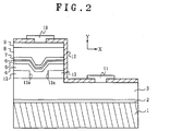
- the semiconductor laser according to the present invention comprises a multi-layer structure in which nitride semiconductor single crystalline layers, represented by (Al x Ga 1-x ) 1-y In y N (0 ⁇ x ⁇ 1,0 ⁇ y ⁇ 1), are stacked in sequence on the substrate 1 composed of sapphire.
- the low-temperature buffer layer 2 composed of AlN, GaN, or the like
- the n-type GaN layer 3 into which Si is doped which composes the conductive layer are disposed in parallel to the substrate.
- two stripe-shaped GaN re-grown layers 13 extend in the direction parallel to the direction (perpendicular to the paper surface) along which the optical cavity is formed.
- the GaN re-grown layers 13 may be an n-type GaN into which Si or the like is doped or a p-type GaN into which Mg or the like is doped.
- the n-type cladding layer 4, the n-type guide layer 5, and the active layer 6 are disposed. Furthermore, the p-type guide layer 7, the p-type cladding layer 8, and the p-type contact layer 9 are disposed in that order.
- the boundary between the n-type cladding layer 4 and the n-type guide layer 5 is a first boundary
- the boundary between the p-type guide layer 7 and the p-type cladding layer 8 is a second boundary. Then, the second boundary of the bent portion is located below the first boundary excluding the bent portion.
- the p-side electrode 10 and the n-side electrode 11 are disposed on the p-type contact layer 9 and the n-type GaN layer 3, respectively, and thus, constitute a semiconductor laser.
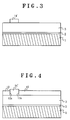
- the sapphire substrate 1 is loaded into a metal organic chemical vapor deposition (MOCVD) furnace (not shown), and then the AlN or GaN buffer layer 2 is deposited on surface a or surface c of the sapphire at a low temperature.
- the deposition is performed by means of the metal organic chemical vapor deposition (MOCVD) method.
- MOCVD metal organic chemical vapor deposition
- the n-type GaN layer 3 into which Si or the like has been doped is stacked by approximately 4 ⁇ m by means of the MOCVD method to fabricate a base substrate.
- the MOCVD method is employed as the deposition method unless otherwise specified.
- the base substrate is taken out of the MOCVD deposition furnace and then a SiO 2 layer is deposited on the top by the sputtering method.
- the SiO 2 layer is deposited such that the thickness thereof is thicker than the optical waveguide layers comprising the active layer 6 and the guide layers 5 and 7 as described later.
- the layer is deposited also to have enough thickness to allow steps to be formed on part of the optical waveguide layers. For example, where the active layer is 0.1 ⁇ m in thickness, and the p- and n-type guide layers are 0.1 ⁇ m in thickness, respectively (that is, the optical waveguide layers are 0.3 ⁇ m in thickness), the layer requires a thickness of 0.3 ⁇ m or more.
- the stacked SiO 2 layer is patterned into the shape of a stripe by the photolithography method to form a SiO 2 mask 14.
- a a wet etching using hydrofluoric acid or a dry etching may be employed as the patterning process.
- the stripe is oriented to ⁇ 11-20 ⁇ of the n-type GaN layer.
- the stripe serves to form the interstitial portions 13a formed between the GaN re-grown layers 13, as described below, thereby the width of the stripe define the width of the bent portions of the optical waveguide layers.
- the bent portions is an optical waveguide for confining the lateral transverse mode. Therefore, the width may be preferably 2 to 10 ⁇ m.
- the substrate is loaded again to the MOCVD deposition furnace and the surface of the substrated is cleaned in an ammonia flow at a temperature of 1050°C.
- the GaN re-grown layers 13 are deposited on the n-type GaN layer 3 partially covered with the SiO 2 mask 14.
- the GaN re-grown layers 13 are grown selectively on portions where the SiO 2 mask 14 is not present, and must not be deposited to greatly exceed the thickness of the SiO 2 mask 14 so as not to hang over the SiO 2 mask 14.
- the GaN re-grown layers 13 may be doped with Si or with Mg.
- the substrate is taken out of the furnace to remove the SiO 2 mask 14 using hydrofluoric acid, which leads to a configuration having the p-type GaN re-grown layers 13 with the interstitial portions 13a.
- the aforementioned GaN re-grown layers 13 are doped with Mg, a semiconductor laser device thus obtained allows current to selectively flow through the interstitial portions 13a.
- providing a higher potential for the side of the n-type cladding layer 4 will cause the PN junction to be biased backward. This will not allow current to flow through the GaN re-grown layers 13, thereby enabling fabrication of a narrow structure of current into the interstitial portions 13a.
- This enables providing preferably an improved light-emitting characteristic of the laser device.
- the substrate is loaded again into the MOCVD deposition furnace and the surface of the substrate is cleaned in an ammonia air current at a temperature of 1050°C.
- the n-type AlGaN cladding layer 4, the n-type GaN guide layer 5, and the active layer 6 are deposited in sequence.
- the p-type GaN guide layer 7, and the p-type AlGaN cladding layer 8, and the p-type GaN contact layer 9 are stacked.
- a layer into which Mg has been doped is activated to perform annealing to turn it into a p-type layer.
- ridges are formed by means of RIE or the like to allow the n-type GaN layer 3 to be exposed, and the SiO 2 insulating layer 12 layer is formed on other layers to provide windows for partially forming electrodes.
- a semiconductor laser is obtained by the p-side electrode 10 and the n-side electrode 11 on the p-type contact layer 9 and the n-type GaN layer 3 via the windows, respectively.
- the present invention allows for forming the optical waveguide layers that are bent as described in the foregoing, while maintaining a good crystalline quality.
- the present invention provides stable characteristics of the lateral transverse mode without accompanying deterioration in the lasing characteristics such as an increase in the threshold current caused by the damage of the crystalline structure of the semiconductor laser obtained.
Landscapes
- Physics & Mathematics (AREA)
- Optics & Photonics (AREA)
- Chemical & Material Sciences (AREA)
- Engineering & Computer Science (AREA)
- Nanotechnology (AREA)
- Condensed Matter Physics & Semiconductors (AREA)
- General Physics & Mathematics (AREA)
- Electromagnetism (AREA)
- Life Sciences & Earth Sciences (AREA)
- Biophysics (AREA)
- Crystallography & Structural Chemistry (AREA)
- Semiconductor Lasers (AREA)
Abstract
Description
Claims (42)
- A method for fabricating a GaN-based semiconductor laser comprising the steps of:forming a first mask on a first conductive layer composed of an n-type semiconductor,depositing a second conductive layer of a thickness not exceeding the thickness of said first mask,removing said first mask,depositing an n-type cladding layer,depositing optical waveguide layers including at least an active layer, anddepositing a p-type cladding layer.
- The method for fabricating a semiconductor laser according to Claim 1, wherein the step of forming said optical waveguide layers further comprises the steps of:depositing an n-type guide layer,depositing an active layer, anddepositing a p-type guide layer.
- The method for fabricating a semiconductor laser according to Claim 2, wherein the thickness of said second conductive layer is thicker than that of said optical waveguide layers.
- The method for fabricating a semiconductor laser according to Claim 3, wherein the step of forming said first mask further comprises the steps of:depositing a mask layer on said first conductive layer and a second stripe-shaped mask on said mask layer,removing said mask layer excluding the portions with which said second mask is covered, andremoving said second mask.
- The method for fabricating a semiconductor laser according to Claim 4, wherein said first mask is formed in parallel to a direction 〈11-20〉 of said first conductive layer.
- The method for fabricating a semiconductor laser according to Claim 5, wherein said first mask is composed of silicon dioxide.
- The method for fabricating a semiconductor laser according to Claim 6, wherein said second conductive layer is composed of a p-type semiconductor.
- A GaN-based semiconductor laser according to the fabrication method of Claim 1, including at least on a conductive layer a multi-layer structure wherein an n-type cladding layer, optical waveguide layers including at least an active layer, and a p-type cladding layer are stacked in that order,
wherein a part of said optical waveguide layers comprises a bent portion which forms stripe-shaped steps which extend in parallel to a direction along which an optical cavity is formed,said conductive layer comprises a first conductive layer and a second conductive layer on top thereof,said first conductive layer is composed of an n-type semiconductor, andsaid second conductive layer comprises two stripe-shaped bodies which extend in parallel to a direction along which an optical cavity is formed. - The semiconductor laser according to Claim 8, wherein the upper boundary of said optical waveguide layers in said bent portion is located further below the lower boundary of said optical waveguide layers excluding said bent portion.
- The method for fabricating a semiconductor laser according to Claim 4, wherein said first mask is composed of silicon dioxide.
- The method for fabricating a semiconductor laser according to Claim 3, wherein said first mask is formed in parallel to a direction 〈11-20〉 of said first conductive layer.
- The method for fabricating a semiconductor laser according to Claim 2, wherein the step of forming said first mask further comprises the steps of:depositing a mask layer on said first conductive layer and a second stripe-shaped mask on said mask layer,removing said mask layer excluding the portions with which said second mask is covered, andremoving said second mask.
- The method for fabricating a semiconductor laser according to Claim 12, wherein said first mask is formed in parallel to a direction 〈11-20〉 of said first conductive layer.
- The method for fabricating a semiconductor laser according to Claim 2, wherein said first mask is formed in parallel to a direction 〈11-20〉 of said first conductive layer.
- The method for fabricating a semiconductor laser according to Claim 2, wherein said first mask is composed of silicon dioxide.
- A GaN-based semiconductor laser according to the fabrication method of Claim 15, including at least on a conductive layer a multi-layer structure wherein an n-type cladding layer, optical waveguide layers including at least an active layer, and a p-type cladding layer are stacked in that order,
wherein a part of said optical waveguide layers comprises a bent portion which forms stripe-shaped steps which extend in parallel to a direction along which an optical cavity is formed,said conductive layer comprises a first conductive layer and a second conductive layer on top thereof,said first conductive layer is composed of an n-type semiconductor, andsaid second conductive layer comprises two stripe-shaped bodies which extend in parallel to a direction along which an optical cavity is formed. - The semiconductor laser according to Claim 16, wherein the upper boundary of said optical waveguide layers in said bent portion is located further below the lower boundary of said optical waveguide layers excluding said bent portion.
- The method for fabricating a semiconductor laser according to Claim 2, wherein said second conductive layer is composed of a p-type semiconductor.
- A GaN-based semiconductor laser according to the fabrication method of Claim 18, including at least on a conductive layer a multi-layer structure wherein an n-type cladding layer, optical waveguide layers including at least an active layer, and a p-type cladding layer are stacked in that order,
wherein a part of said optical waveguide layers comprises a bent portion which forms stripe-shaped steps which extend in parallel to a direction along which an optical cavity is formed,said conductive layer comprises a first conductive layer and a second conductive layer on top thereof,said first conductive layer is composed of an n-type semiconductor, andsaid second conductive layer comprises two stripe-shaped bodies which extend in parallel to a direction along which an optical cavity is formed. - The semiconductor laser according to Claim 19, wherein the upper boundary of said optical waveguide layers in said bent portion is located further below the lower boundary of said optical waveguide layers excluding said bent portion.
- A GaN-based semiconductor laser according to the fabrication method of Claim 2, including at least on a conductive layer a multi-layer structure wherein an n-type cladding layer, optical waveguide layers including at least an active layer, and a p-type cladding layer are stacked in that order,
wherein a part of said optical waveguide layers comprises a bent portion which forms stripe-shaped steps which extend in parallel to a direction along which an optical cavity is formed,said conductive layer comprises a first conductive layer and a second conductive layer on top thereof,said first conductive layer is composed of an n-type semiconductor, andsaid second conductive layer comprises two stripe-shaped bodies which extend in parallel to a direction along which an optical cavity is formed. - The semiconductor laser according to Claim 21, wherein the upper boundary of said optical waveguide layers in said bent portion is located further below the lower boundary of said optical waveguide layers excluding said bent portion.
- The method for fabricating a semiconductor laser according to Claim 1, wherein the thickness of said second conductive layer is thicker than that of said optical waveguide layers.
- The method for fabricating a semiconductor laser according to Claim 23, wherein the step of forming said first mask further comprises the steps of:depositing a mask layer on said first conductive layer and a second stripe-shaped mask on said mask layer,removing said mask layer excluding the portions with which said second mask is covered, andremoving said second mask.
- The method for fabricating a semiconductor laser according to Claim 24, wherein said first mask is formed in parallel to a direction 〈11-20〉 of said first conductive layer.
- The method for fabricating a semiconductor laser according to Claim 25, wherein said first mask is composed of silicon dioxide.
- The method for fabricating a semiconductor laser according to Claim 26, wherein said second conductive layer is composed of a p-type semiconductor.
- A GaN-based semiconductor laser according to the fabrication method of Claim 27, including at least on a conductive layer a multi-layer structure wherein an n-type cladding layer, optical waveguide layers including at least an active layer, and a p-type cladding layer are stacked in that order,
wherein a part of said optical waveguide layers comprises a bent portion which forms stripe-shaped steps which extend in parallel to a direction along which an optical cavity is formed,said conductive layer comprises a first conductive layer and a second conductive layer on top thereof,said first conductive layer is composed of an n-type semiconductor, andsaid second conductive layer comprises two stripe-shaped bodies which extend in parallel to a direction along which an optical cavity is formed. - The semiconductor laser according to Claim 28, wherein the upper boundary of said optical waveguide layers in said bent portion is located further below the lower boundary of said optical waveguide layers excluding said bent portion.
- The method for fabricating a semiconductor laser according to Claim 24, wherein said first mask is composed of silicon dioxide.
- The method for fabricating a semiconductor laser according to Claim 23, wherein said first mask is formed in parallel to a direction 〈11-20〉 of said first conductive layer.
- The method for fabricating a semiconductor laser according to Claim 1, wherein the step of forming said first mask further comprises the steps of:depositing a mask layer on said first conductive layer and a second stripe-shaped mask on said mask layer,removing said mask layer excluding the portions with which said second mask is covered, andremoving said second mask.
- The method for fabricating a semiconductor laser according to Claim 32, wherein said first mask is formed in parallel to a direction 〈11-20〉 of said first conductive layer.
- The method for fabricating a semiconductor laser according to Claim 1, wherein said first mask is formed in parallel to a direction 〈11-20〉 of said first conductive layer.
- The method for fabricating a semiconductor laser according to Claim 1, wherein said first mask is composed of silicon dioxide.
- A GaN-based semiconductor laser according to the fabrication method of Claim 35, including at least on a conductive layer a multi-layer structure wherein an n-type cladding layer, optical waveguide layers including at least an active layer, and a p-type cladding layer are stacked in that order,
wherein a part of said optical waveguide layers comprises a bent portion which forms stripe-shaped steps which extend in parallel to a direction along which an optical cavity is formed,said conductive layer comprises a first conductive layer and a second conductive layer on top thereof,said first conductive layer is composed of an n-type semiconductor, andsaid second conductive layer comprises two stripe-shaped bodies which extend in parallel to a direction along which an optical cavity is formed. - The semiconductor laser according to Claim 36, wherein the upper boundary of said optical waveguide layers in said bent portion is located further below the lower boundary of said optical waveguide layers excluding said bent portion.
- The method for fabricating a semiconductor laser according to Claim 1, wherein said second conductive layer is composed of a p-type semiconductor.
- A GaN-based semiconductor laser according to the fabrication method of Claim 38, including at least on a conductive layer a multi-layer structure wherein an n-type cladding layer, optical waveguide layers including at least an active layer, and a p-type cladding layer are stacked in that order,
wherein a part of said optical waveguide layers comprises a bent portion which forms stripe-shaped steps which extend in parallel to a direction along which an optical cavity is formed,said conductive layer comprises a first conductive layer and a second conductive layer on top thereof,said first conductive layer is composed of an n-type semiconductor, andsaid second conductive layer comprises two stripe-shaped bodies which extend in parallel to a direction along which an optical cavity is formed. - The semiconductor laser according to Claim 39, wherein the upper boundary of said optical waveguide layers in said bent portion is located further below the lower boundary of said optical waveguide layers excluding said bent portion.
- A GaN-based semiconductor laser according to the fabrication method of Claim 1, including at least on a conductive layer a multi-layer structure wherein an n-type cladding layer, optical waveguide layers including at least an active layer, and a p-type cladding layer are stacked in that order,
wherein a part of said optical waveguide layers comprises a bent portion which forms stripe-shaped steps which extend in parallel to a direction along which an optical cavity is formed,said conductive layer comprises a first conductive layer and a second conductive layer on top thereof,said first conductive layer is composed of an n-type semiconductor, andsaid second conductive layer comprises two stripe-shaped bodies which extend in parallel to a direction along which an optical cavity is formed. - The semiconductor laser according to Claim 41, wherein the upper boundary of said optical waveguide layers in said bent portion is located further below the lower boundary of said optical waveguide layers excluding said bent portion.
Applications Claiming Priority (2)
| Application Number | Priority Date | Filing Date | Title |
|---|---|---|---|
| JP2380599 | 1999-02-01 | ||
| JP02380599A JP3690570B2 (en) | 1999-02-01 | 1999-02-01 | Semiconductor laser device and manufacturing method thereof |
Publications (3)
| Publication Number | Publication Date |
|---|---|
| EP1026799A2 true EP1026799A2 (en) | 2000-08-09 |
| EP1026799A3 EP1026799A3 (en) | 2000-08-23 |
| EP1026799B1 EP1026799B1 (en) | 2002-04-10 |
Family
ID=12120553
Family Applications (1)
| Application Number | Title | Priority Date | Filing Date |
|---|---|---|---|
| EP00101635A Expired - Lifetime EP1026799B1 (en) | 1999-02-01 | 2000-01-31 | Semiconductor laser and fabricating method therefor |
Country Status (4)
| Country | Link |
|---|---|
| US (1) | US20030021316A1 (en) |
| EP (1) | EP1026799B1 (en) |
| JP (1) | JP3690570B2 (en) |
| DE (1) | DE60000115T2 (en) |
Families Citing this family (1)
| Publication number | Priority date | Publication date | Assignee | Title |
|---|---|---|---|---|
| US20030235225A1 (en) * | 2002-06-22 | 2003-12-25 | Rick Glew | Guided self-aligned laser structure with integral current blocking layer |
Family Cites Families (2)
| Publication number | Priority date | Publication date | Assignee | Title |
|---|---|---|---|---|
| JP3060973B2 (en) * | 1996-12-24 | 2000-07-10 | 日本電気株式会社 | Manufacturing method of gallium nitride based semiconductor laser using selective growth method and gallium nitride based semiconductor laser |
| JPH1117277A (en) * | 1997-06-20 | 1999-01-22 | Sharp Corp | Nitride-based semiconductor laser device and method of manufacturing the same |
-
1999
- 1999-02-01 JP JP02380599A patent/JP3690570B2/en not_active Expired - Fee Related
-
2000
- 2000-01-31 DE DE60000115T patent/DE60000115T2/en not_active Expired - Lifetime
- 2000-01-31 EP EP00101635A patent/EP1026799B1/en not_active Expired - Lifetime
- 2000-01-31 US US09/494,647 patent/US20030021316A1/en not_active Abandoned
Also Published As
| Publication number | Publication date |
|---|---|
| DE60000115T2 (en) | 2002-08-22 |
| JP2000223783A (en) | 2000-08-11 |
| EP1026799A3 (en) | 2000-08-23 |
| DE60000115D1 (en) | 2002-05-16 |
| EP1026799B1 (en) | 2002-04-10 |
| JP3690570B2 (en) | 2005-08-31 |
| US20030021316A1 (en) | 2003-01-30 |
Similar Documents
| Publication | Publication Date | Title |
|---|---|---|
| US6319742B1 (en) | Method of forming nitride based semiconductor layer | |
| KR100763829B1 (en) | Semiconductor laser device, and method of manufacturing the same | |
| JP3060973B2 (en) | Manufacturing method of gallium nitride based semiconductor laser using selective growth method and gallium nitride based semiconductor laser | |
| JP3822976B2 (en) | Semiconductor device and manufacturing method thereof | |
| JP4540347B2 (en) | Nitride semiconductor laser device and manufacturing method thereof | |
| JP2002009004A (en) | Method for manufacturing nitride semiconductor, method for manufacturing nitride semiconductor device, nitride semiconductor device, semiconductor light emitting device, and method for manufacturing the same | |
| KR100539289B1 (en) | Semiconductor light-emitting device and the method for producing thereof | |
| EP1005124A2 (en) | Semiconductor light emitting device and its manufacturing method | |
| US6337223B1 (en) | Semiconductor optical device and method for fabricating the same | |
| JPH11260737A (en) | Manufacture of semiconductor substrate and semiconductor light emitting element | |
| JP3796060B2 (en) | Semiconductor laser device and manufacturing method thereof | |
| JP4608731B2 (en) | Manufacturing method of semiconductor laser | |
| JP2011023453A (en) | Method for manufacturing semiconductor device | |
| EP1026799B1 (en) | Semiconductor laser and fabricating method therefor | |
| JP2000299530A (en) | Semiconductor light-emitting device | |
| JP4415440B2 (en) | Manufacturing method of semiconductor laser | |
| JP2006093682A (en) | Semiconductor laser and manufacturing method thereof | |
| JP2000091696A (en) | Semiconductor element, semiconductor light-emitting element and manufacture thereof | |
| JP3244312B2 (en) | AlGaInP-based visible light semiconductor laser device | |
| EP0955709A2 (en) | Blue edge emitting laser | |
| JP2003179314A (en) | Nitride-based semiconductor light emitting device and method of manufacturing the same | |
| JP2001144374A (en) | Semiconductor laser device | |
| JP2000244071A (en) | Semiconductor light-emitting element and its manufacture | |
| JP2000183463A (en) | Semiconductor laser and its manufacturing method | |
| JPH08264875A (en) | Semiconductor laser device |
Legal Events
| Date | Code | Title | Description |
|---|---|---|---|
| PUAI | Public reference made under article 153(3) epc to a published international application that has entered the european phase |
Free format text: ORIGINAL CODE: 0009012 |
|
| PUAL | Search report despatched |
Free format text: ORIGINAL CODE: 0009013 |
|
| AK | Designated contracting states |
Kind code of ref document: A2 Designated state(s): DE FR GB |
|
| AX | Request for extension of the european patent |
Free format text: AL;LT;LV;MK;RO;SI |
|
| AK | Designated contracting states |
Kind code of ref document: A3 Designated state(s): AT BE CH CY DE DK ES FI FR GB GR IE IT LI LU MC NL PT SE |
|
| AX | Request for extension of the european patent |
Free format text: AL;LT;LV;MK;RO;SI |
|
| 17P | Request for examination filed |
Effective date: 20001018 |
|
| 17Q | First examination report despatched |
Effective date: 20001123 |
|
| GRAG | Despatch of communication of intention to grant |
Free format text: ORIGINAL CODE: EPIDOS AGRA |
|
| AKX | Designation fees paid |
Free format text: DE FR GB |
|
| GRAG | Despatch of communication of intention to grant |
Free format text: ORIGINAL CODE: EPIDOS AGRA |
|
| GRAH | Despatch of communication of intention to grant a patent |
Free format text: ORIGINAL CODE: EPIDOS IGRA |
|
| GRAH | Despatch of communication of intention to grant a patent |
Free format text: ORIGINAL CODE: EPIDOS IGRA |
|
| REG | Reference to a national code |
Ref country code: GB Ref legal event code: IF02 |
|
| GRAA | (expected) grant |
Free format text: ORIGINAL CODE: 0009210 |
|
| AK | Designated contracting states |
Kind code of ref document: B1 Designated state(s): DE FR GB |
|
| REF | Corresponds to: |
Ref document number: 60000115 Country of ref document: DE Date of ref document: 20020516 |
|
| ET | Fr: translation filed | ||
| REG | Reference to a national code |
Ref country code: GB Ref legal event code: 746 Effective date: 20021118 |
|
| PLBE | No opposition filed within time limit |
Free format text: ORIGINAL CODE: 0009261 |
|
| STAA | Information on the status of an ep patent application or granted ep patent |
Free format text: STATUS: NO OPPOSITION FILED WITHIN TIME LIMIT |
|
| 26N | No opposition filed |
Effective date: 20030113 |
|
| REG | Reference to a national code |
Ref country code: FR Ref legal event code: D6 |
|
| PGFP | Annual fee paid to national office [announced via postgrant information from national office to epo] |
Ref country code: FR Payment date: 20110128 Year of fee payment: 12 Ref country code: DE Payment date: 20110126 Year of fee payment: 12 |
|
| PGFP | Annual fee paid to national office [announced via postgrant information from national office to epo] |
Ref country code: GB Payment date: 20110126 Year of fee payment: 12 |
|
| GBPC | Gb: european patent ceased through non-payment of renewal fee |
Effective date: 20120131 |
|
| REG | Reference to a national code |
Ref country code: FR Ref legal event code: ST Effective date: 20120928 |
|
| PG25 | Lapsed in a contracting state [announced via postgrant information from national office to epo] |
Ref country code: GB Free format text: LAPSE BECAUSE OF NON-PAYMENT OF DUE FEES Effective date: 20120131 Ref country code: DE Free format text: LAPSE BECAUSE OF NON-PAYMENT OF DUE FEES Effective date: 20120801 |
|
| REG | Reference to a national code |
Ref country code: DE Ref legal event code: R119 Ref document number: 60000115 Country of ref document: DE Effective date: 20120801 |
|
| PG25 | Lapsed in a contracting state [announced via postgrant information from national office to epo] |
Ref country code: FR Free format text: LAPSE BECAUSE OF NON-PAYMENT OF DUE FEES Effective date: 20120131 |