EP1026747B1 - Image sensor - Google Patents
Image sensor Download PDFInfo
- Publication number
- EP1026747B1 EP1026747B1 EP00300516A EP00300516A EP1026747B1 EP 1026747 B1 EP1026747 B1 EP 1026747B1 EP 00300516 A EP00300516 A EP 00300516A EP 00300516 A EP00300516 A EP 00300516A EP 1026747 B1 EP1026747 B1 EP 1026747B1
- Authority
- EP
- European Patent Office
- Prior art keywords
- subpixels
- readout
- layer
- colour
- subpixel
- Prior art date
- Legal status (The legal status is an assumption and is not a legal conclusion. Google has not performed a legal analysis and makes no representation as to the accuracy of the status listed.)
- Expired - Lifetime
Links
- 238000004891 communication Methods 0.000 claims description 16
- WYTGDNHDOZPMIW-RCBQFDQVSA-N alstonine Natural products C1=CC2=C3C=CC=CC3=NC2=C2N1C[C@H]1[C@H](C)OC=C(C(=O)OC)[C@H]1C2 WYTGDNHDOZPMIW-RCBQFDQVSA-N 0.000 claims description 15
- 238000009826 distribution Methods 0.000 claims description 15
- 229910021417 amorphous silicon Inorganic materials 0.000 claims description 8
- 239000003989 dielectric material Substances 0.000 claims description 8
- 239000004065 semiconductor Substances 0.000 claims description 8
- 239000000758 substrate Substances 0.000 claims description 8
- 239000003086 colorant Substances 0.000 claims description 6
- 230000003287 optical effect Effects 0.000 claims description 4
- 238000010521 absorption reaction Methods 0.000 claims description 2
- 239000010410 layer Substances 0.000 description 96
- 238000013461 design Methods 0.000 description 5
- 238000000034 method Methods 0.000 description 5
- XUIMIQQOPSSXEZ-UHFFFAOYSA-N Silicon Chemical compound [Si] XUIMIQQOPSSXEZ-UHFFFAOYSA-N 0.000 description 4
- 229910052710 silicon Inorganic materials 0.000 description 4
- 239000010703 silicon Substances 0.000 description 4
- 238000003384 imaging method Methods 0.000 description 3
- VYPSYNLAJGMNEJ-UHFFFAOYSA-N Silicium dioxide Chemical compound O=[Si]=O VYPSYNLAJGMNEJ-UHFFFAOYSA-N 0.000 description 2
- 239000004411 aluminium Substances 0.000 description 2
- 229910052782 aluminium Inorganic materials 0.000 description 2
- XAGFODPZIPBFFR-UHFFFAOYSA-N aluminium Chemical compound [Al] XAGFODPZIPBFFR-UHFFFAOYSA-N 0.000 description 2
- 230000002860 competitive effect Effects 0.000 description 2
- 238000007639 printing Methods 0.000 description 2
- WFKWXMTUELFFGS-UHFFFAOYSA-N tungsten Chemical compound [W] WFKWXMTUELFFGS-UHFFFAOYSA-N 0.000 description 2
- 229910052721 tungsten Inorganic materials 0.000 description 2
- 239000010937 tungsten Substances 0.000 description 2
- 229910052581 Si3N4 Inorganic materials 0.000 description 1
- 239000000654 additive Substances 0.000 description 1
- 230000000996 additive effect Effects 0.000 description 1
- 230000003321 amplification Effects 0.000 description 1
- 238000013459 approach Methods 0.000 description 1
- 230000015556 catabolic process Effects 0.000 description 1
- 239000004020 conductor Substances 0.000 description 1
- 238000006731 degradation reaction Methods 0.000 description 1
- 238000000151 deposition Methods 0.000 description 1
- 238000005516 engineering process Methods 0.000 description 1
- 238000005530 etching Methods 0.000 description 1
- 230000017525 heat dissipation Effects 0.000 description 1
- AMGQUBHHOARCQH-UHFFFAOYSA-N indium;oxotin Chemical compound [In].[Sn]=O AMGQUBHHOARCQH-UHFFFAOYSA-N 0.000 description 1
- 239000012212 insulator Substances 0.000 description 1
- 238000004519 manufacturing process Methods 0.000 description 1
- 239000011159 matrix material Substances 0.000 description 1
- 229910052751 metal Inorganic materials 0.000 description 1
- 239000002184 metal Substances 0.000 description 1
- 150000002739 metals Chemical class 0.000 description 1
- 238000003199 nucleic acid amplification method Methods 0.000 description 1
- 238000000059 patterning Methods 0.000 description 1
- 238000000206 photolithography Methods 0.000 description 1
- 238000012545 processing Methods 0.000 description 1
- 238000009416 shuttering Methods 0.000 description 1
- 235000012239 silicon dioxide Nutrition 0.000 description 1
- 239000000377 silicon dioxide Substances 0.000 description 1
- HQVNEWCFYHHQES-UHFFFAOYSA-N silicon nitride Chemical compound N12[Si]34N5[Si]62N3[Si]51N64 HQVNEWCFYHHQES-UHFFFAOYSA-N 0.000 description 1
- 239000002356 single layer Substances 0.000 description 1
Images


Classifications
-
- H—ELECTRICITY
- H01—ELECTRIC ELEMENTS
- H01L—SEMICONDUCTOR DEVICES NOT COVERED BY CLASS H10
- H01L27/00—Devices consisting of a plurality of semiconductor or other solid-state components formed in or on a common substrate
- H01L27/14—Devices consisting of a plurality of semiconductor or other solid-state components formed in or on a common substrate including semiconductor components sensitive to infrared radiation, light, electromagnetic radiation of shorter wavelength or corpuscular radiation and specially adapted either for the conversion of the energy of such radiation into electrical energy or for the control of electrical energy by such radiation
- H01L27/144—Devices controlled by radiation
- H01L27/146—Imager structures
- H01L27/14601—Structural or functional details thereof
- H01L27/14603—Special geometry or disposition of pixel-elements, address-lines or gate-electrodes
-
- H—ELECTRICITY
- H01—ELECTRIC ELEMENTS
- H01L—SEMICONDUCTOR DEVICES NOT COVERED BY CLASS H10
- H01L27/00—Devices consisting of a plurality of semiconductor or other solid-state components formed in or on a common substrate
- H01L27/14—Devices consisting of a plurality of semiconductor or other solid-state components formed in or on a common substrate including semiconductor components sensitive to infrared radiation, light, electromagnetic radiation of shorter wavelength or corpuscular radiation and specially adapted either for the conversion of the energy of such radiation into electrical energy or for the control of electrical energy by such radiation
- H01L27/144—Devices controlled by radiation
- H01L27/146—Imager structures
- H01L27/14601—Structural or functional details thereof
- H01L27/1462—Coatings
- H01L27/14621—Colour filter arrangements
-
- H—ELECTRICITY
- H01—ELECTRIC ELEMENTS
- H01L—SEMICONDUCTOR DEVICES NOT COVERED BY CLASS H10
- H01L27/00—Devices consisting of a plurality of semiconductor or other solid-state components formed in or on a common substrate
- H01L27/14—Devices consisting of a plurality of semiconductor or other solid-state components formed in or on a common substrate including semiconductor components sensitive to infrared radiation, light, electromagnetic radiation of shorter wavelength or corpuscular radiation and specially adapted either for the conversion of the energy of such radiation into electrical energy or for the control of electrical energy by such radiation
- H01L27/144—Devices controlled by radiation
- H01L27/146—Imager structures
- H01L27/14601—Structural or functional details thereof
- H01L27/1462—Coatings
- H01L27/14623—Optical shielding
-
- H—ELECTRICITY
- H01—ELECTRIC ELEMENTS
- H01L—SEMICONDUCTOR DEVICES NOT COVERED BY CLASS H10
- H01L27/00—Devices consisting of a plurality of semiconductor or other solid-state components formed in or on a common substrate
- H01L27/14—Devices consisting of a plurality of semiconductor or other solid-state components formed in or on a common substrate including semiconductor components sensitive to infrared radiation, light, electromagnetic radiation of shorter wavelength or corpuscular radiation and specially adapted either for the conversion of the energy of such radiation into electrical energy or for the control of electrical energy by such radiation
- H01L27/144—Devices controlled by radiation
- H01L27/146—Imager structures
- H01L27/14601—Structural or functional details thereof
- H01L27/14625—Optical elements or arrangements associated with the device
- H01L27/14627—Microlenses
-
- H—ELECTRICITY
- H01—ELECTRIC ELEMENTS
- H01L—SEMICONDUCTOR DEVICES NOT COVERED BY CLASS H10
- H01L27/00—Devices consisting of a plurality of semiconductor or other solid-state components formed in or on a common substrate
- H01L27/14—Devices consisting of a plurality of semiconductor or other solid-state components formed in or on a common substrate including semiconductor components sensitive to infrared radiation, light, electromagnetic radiation of shorter wavelength or corpuscular radiation and specially adapted either for the conversion of the energy of such radiation into electrical energy or for the control of electrical energy by such radiation
- H01L27/144—Devices controlled by radiation
- H01L27/146—Imager structures
- H01L27/14643—Photodiode arrays; MOS imagers
-
- H—ELECTRICITY
- H04—ELECTRIC COMMUNICATION TECHNIQUE
- H04N—PICTORIAL COMMUNICATION, e.g. TELEVISION
- H04N25/00—Circuitry of solid-state image sensors [SSIS]; Control thereof
- H04N25/10—Circuitry of solid-state image sensors [SSIS]; Control thereof for transforming different wavelengths into image signals
- H04N25/11—Arrangement of colour filter arrays [CFA]; Filter mosaics
- H04N25/13—Arrangement of colour filter arrays [CFA]; Filter mosaics characterised by the spectral characteristics of the filter elements
- H04N25/134—Arrangement of colour filter arrays [CFA]; Filter mosaics characterised by the spectral characteristics of the filter elements based on three different wavelength filter elements
Definitions
- the present invention relates generally to an active image sensor, for example an active image sensor with an amorphous silicon sensing layer and a semiconductor readout layer.
- Imaging systems such as digital cameras, camcorders, scanners, copiers, and the like require an image sensor capable of capturing an image with high resolution and colour fidelity.
- a majority of the imaging systems uses a solid-state image sensor due to constraints on system size, weight, power consumption, heat dissipation, and durability.
- the ability of the imaging system to capture images with high resolution and colour fidelity depends to a large extent on the image sensor used.
- Image sensor resolution is typically measured in number of pixels contained in the image sensor.
- the resolution of a solid-state sensor can be increased by shrinking the size of the pixels so that more pixels fit within a predetermined area. An image incident on an image sensor having more pixels per unit of area can be captured with greater resolution than an image sensor having fewer pixels per unit of area.
- Pixel geometry and symmetry between pixels can also affect the number of pixels per unit of area. Additionally, the symmetry between pixels can affect colour aliasing. Other factors, such as electrical noise generated by the pixels can affect image quality. Additionally, for colour images, the colour fidelity of the image can be affected by a predetermined colour pattern assigned to the pixels in the image sensor.
- Desirable attributes of an image sensor include low electrical noise, flexibility in colour pattern, optimized pixel density and geometry for increased resolution, symmetry between adjacent pixels, and maximized pixel fill-factor.
- Low electrical noise prevents an image signal generated by the pixel from being corrupted by noise; furthermore, noise and leakage current from an individual pixel can affect the image signal from adjacent pixels.
- pixel electrical noise can be affected by pixel geometry and symmetry between pixels. Circuitry or algorithms to filter out the electrical noise can be minimized or eliminated by reducing the noise generated by each pixel.
- a flexible colour pattern allows the image sensor to be tailored to specific applications such as a RGB colour pattern for photography or video, or a CMY colour pattern for printing or scanning, for example.
- Pixels having a rectangular geometry can generate additional noise due to abrupt rectangle edges which create leakage current in an active device such as a photodiode, for example.
- a pixel geometry that eliminates noise due to abrupt edges is desirable. Further, it is desirable to maximise the active area of the pixel devoted to capturing the image so that the ratio of the active area to the pixel area approaches a fill-factor of 100%. By removing components, such as transistors and signal routing lines, from the pixel, the area that was occupied by the components can be used to maximise the active area of the pixel thereby increasing the fill-factor.
- Previous image sensor designs include photo-gate active pixel sensors, bulk silicon photodiode pixel sensors with three transistors, pulsed bipolar CMOS active pixel sensors, and rectangular CMOS pixel sensors.
- the photo-gate active pixel sensor utilises four transistors inside of a CMOS photo-gate pixel for low noise operation and for electronic shuttering. However, this number of transistors results in a pixel area that is not competitive with state-of-the-art CCD image sensors that have pixel areas approaching 5 x 5 ⁇ m 2 . The number of transistors in the photo-gate sensor results in a lower fill-factor when compared to the state-of-the-art CCD image sensor.
- the pulsed bipolar CMOS active pixel sensor employs a vertical bipolar device in a CMOS process.
- the use of bipolar devices results in a smaller pixel area due to fewer transistors in the pixel; however, disadvantages of this design include image lag and the need to amplify an output signal from the pixel with a high ⁇ gain bipolar transistor.
- the high ⁇ gain bipolar transistor exhibits signal degradation under low current conditions and limits scalability of the pixel due to an integrating amplification stage in a readout path of the pixel.
- an extra emitter terminal is required to prevent an overflow condition. The extra emitter terminal creates an unsymmetrical pixel layout in the CMOS process.
- CMOS design rules require adjacent pixels to be spaced apart to comply with design rules for N-well spacing.
- the bulk silicon photodiode pixel sensor is not competitive with the state-of the-art CCD image sensor because the photodiode and the transistors are integral to the same silicon layer and the area occupied by the transistors reduces the active area available for the photodiode resulting in a fill-factor of about 30% using 1.2 ⁇ m CMOS process technology.
- Rectangular CMOS active pixel sensor designs utilise a rectangular pixel geometry with the pixels laid out in a rectangular grid. It is clearly understood that the rectangular grid does not result in an optimized pixel density.
- Bayer's colour pattern was developed as the colour filter array (CFA) pattern for the rectangular grid.
- CFA colour filter array
- colour density for Red, Green, and Blue sensors is in the ratio of 1:2:1. Therefore, there are two Green pixels for each Red pixel and Blue pixel in the array.
- the colour density for the Bayer CFA pattern is not the best choice because it undersamples two of the sensor colors (Red and Blue) and the colour pattern kernel is not symmetric.
- linear horizontal, linear vertical, and linear diagonal image features never pass through more than two different colour sensor locations because the Red and the Blue sensor locations are never adjacent to sensors of the same colour.
- the rectangular pixel geometry is not amenable to flexible colour patterning.
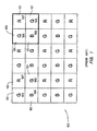
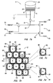
- FIG. 1 there is provided for purposes of illustration a prior art rectangular CMOS active pixel sensor designated generally as 100.
- the sensor 100 has a plurality of subpixels 101. Four of the subpixels 101 define a pixel 103, shown in heavy outline.
- the pixel 103 has two Green subpixels 105, one Red subpixel 107, and one Blue subpixel 109.
- This arrangement of the colour pattern for the subpixels 101 in the pixel 103 corresponds to the Bayer CFA pattern wherein the colour density of the Red subpixel 107, the Green subpixels 105, and the Blue subpixel 109 is in the ratio of 1:2:1, wherein the pixel 103 has two Green subpixels 105 for one Red subpixel 107 and one Blue sub pixel 109.
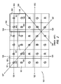
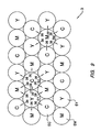
- FIG. 2 illustrates lineal image feature traversals across prior art sensor 100.
- the image feature traverses the Green subpixels 105 and the Red subpixels 107.
- the image feature traverses the Blue subpixels 109 and the Green subpixels 105.
- the first horizontal traverse 133 never crosses the Blue subpixels 109.
- the second horizontal traverse 122 never crosses the Red subpixels 107.
- the first horizontal traverse 133 and the second horizontal traverse 122 never make a sequential crossing of the Red subpixels 107, the Green subpixels 105, and the Blue subpixels 109 in a single traverse of the sensor 100.
- a second vertical traverse as shown by an arrow 124 only the Green subpixels 105 and the Blue subpixels 109 are traversed.
- a first diagonal traverse as shown by an arrow 137 only all the Green subpixels 105 are traversed.
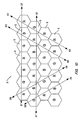
- CMOS photo-gate and photodiode implementations of an active pixel sensor exhibit crosstalk between pixels of different colour due to electron leakage from an electron collection node. Additionally, crosstalk is exacerbated by any non-uniformity in distance between pixels. Such non-uniformity can result in a non-uniform crosstalk pattern especially for different colour channels. Due to the rectangular geometry and the Bayer CFA pattern, a pixel is surrounded by a group of eight pixels. The pixels in the group that are horizontally or vertically adjacent to the surrounded pixel are closer to the surrounded pixel than pixels that are diagonally adjacent to the surrounded pixel resulting in a variation in distance between the surrounded pixel and the other pixels in the group. A non-uniform crosstalk pattern is created by the variation in distance.
- Red subpixel 117 is surrounded by four Green subpixels 125 and four Blue subpixels 129.
- the Blue subpixels 129 are diagonally adjacent to the Red subpixel 117 and are at a greater distance from the Red subpixel 117 than the Green subpixels 125 that are abutted to the Red subpixel 117.
- Blue subpixel 119 is surrounded by four Green subpixels 125 and four Red subpixels 127 with the Red subpixels 127 positioned diagonal to and at a greater distance from the Blue subpixel 119 than the Green subpixels 125.
- Green subpixels 125 are abutted to the Blue subpixel 119 and are therefore closer in distance to the Blue subpixel 119 than the Red subpixels 127.
- Green subpixel 115 is surrounded by two Red subpixels 127, two Blue subpixels 129, and four Green subpixels 125.
- the two Red subpixels 127 and the two Blue subpixels 129 are abutted to the Green subpixel 115, whereas the four Green subpixels 125 are positioned diagonal to the Green subpixel 115. Because of the oversampling of Green by a factor of two to one over Red and Blue in the Bayer CFA pattern, the Green subpixel 115 is surrounded by four Green subpixels 125.
- the extra distance between the surrounded pixel and diagonally adjacent pixels can result in a non-uniform cross talk pattern.
- the non-uniform cross talk pattern can be exacerbated because the Green subpixel 115 is not surrounded by an equal number of subpixels having the same colour.
- the two Blue subpixels 129 and the two Red subpixels 127 may not have cross talk patterns that cancel, resulting in additional cross talk due to colour imbalance that is additive with the cross talk due to the extra distance of the four Green subpixels 125 that are diagonal to the Green subpixel 115.
- US 5,619,033 discloses a photodetecting device with at least one photodiode formed over and coupled to a transistor.
- the photodetecting devices are formed in a matrix.
- Each photodiode is separated from adjacent photodiodes by notches which may be formed in any two dimensional polygonal pattern such as triangular or hexagonal patterns.
- the present invention seeks to provide an improved image sensor.
- an image sensor as specified in claim 1.
- an active image sensor in which photodiodes are laid out in a geometrically-efficient pattern, preferably hexagonal as opposed to rectilinear, and in which the photodiodes and their associated amplifiers are stacked vertically.
- Such an image sensor has a higher pixel density than the other sensors and offers higher resolution, better colour fidelity, less noise, less crosstalk, and a more flexible CFA pattern.
- the image sensor includes a semiconductor substrate having a plurality of readout cells formed in the substrate.
- the substrate defines a readout layer with the readout cells positioned in rows.
- Each readout cell has a signal input.
- a dielectric material is formed on the readout layer to define a sensing layer.
- a plurality of cavities are formed in the sensing layer. The cavities are arranged in a hexagonal grid layout and are positioned in opposing relation to the readout cells in the readout layer.
- An amorphous silicon P-I-N photodiode is formed in each cavity of the sensing layer. Each photodiode generates an output signal indicative of light incident on the photodiode.
- An interconnect communicates the output signal from the photodiode to the signal input of the readout cell.
- a biased optically transparent electrode is disposed in each cavity and operates to bias the photodiode and allows light incident on the electrode to be imaged onto the photodiode.
- the photodiode and the electrode define a subpixel of the sensing layer.
- An amplifier is disposed in each readout cell vertically stacked beneath an associated photodiode and in electrical communication therewith to amplify the signal from that photodiode. Placing the amplifier beneath its associated photodiode eliminates signal routing lines, transistors, and other components from the active area of the photodiode thereby maximising the area of the photodiode available for receiving incident light.
- An opaque optical shield may be used to prevent light incident on the photodiode from impinging on the readout layer.
- the subpixel is preferably shaped so as to optimise subpixel density in the sensing layer.
- a hexagonal shape works well, but another suitable shape such as a circular shape may be used.
- the readout layer has a serpentine bus and a stair-step bus.
- the serpentine bus and the stair-step bus are defined by a row having a first pattern of signal routing and an adjacent row having a second pattern of signal routing. The first and second patterns align to form the serpentine bus and the stair-step bus.
- the serpentine bus and the stair-step bus are extended throughout the readout layer. As mentioned above, the active area of the photodiode in the sensing layer is maximized by placing the signal routing in the readout layer.
- the sensing layer may include a filter layer positioned adjacent to the electrode.
- the filter layer is a colour filter.
- the colour filter may be varied among the subpixels to produce a desired colour pattern or to create symmetry or asymmetry in the colour filter pattern among adjacent subpixels.
- the sensing layer may include an infrared filter to attenuate the absorption of infrared noise from the light incident on the subpixel.
- the sensing layer includes a microlens positioned adjacent the subpixel for focusing incident light onto the subpixel.
- the preferred embodiment is an image sensor including a semiconductor substrate defining a readout layer and a dielectric material defining a sensing layer.
- the readout layer has a plurality of readout cells formed in the substrate an arranged in rows. The readout cells in a row are offset in position with respect to the readout cells in an adjacent row. Each readout cell has a signal input.
- the dielectric material is formed on the readout layer to define the sensing layer.
- a plurality of cavities are formed in the sensing layer. The cavities are arranged in a hexagonal grid layout and are positioned in opposing relation to the readout cells in the readout layer. A portion of each cavity has an opening in communication with the signal input of the readout cell.
- An amorphous silicon P-I-N photodiode is formed in each cavity and defines a subpixel of the image sensor. Each photodiode generates an output signal indicative of light incident thereon.
- An interconnect positioned in the opening of each cavity communicates the output signal from the photodiode to the signal input of the readout cell.
- a biased optically transparent electrode is disposed in the cavity and operates to bias the photodiode and allows light incident on the electrode to be imaged onto the photodiode.
- the photodiode and the electrode define a subpixel.
- the image sensor has an optimal subpixel density, maximises subpixel fill-factor, has a flexible subpixel geometry, can be implemented with a variety of colour patterns, reduces electrical noise and crosstalk, and provides for uniform spacing and symmetry between subpixels.
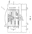
- FIG. 4 there is shown an embodiment of image sensor which includes a semiconductor substrate that defines a readout layer 17.
- the readout layer 17 has a plurality of readout cells 20 formed therein.
- FIG. 4 illustrates one readout cell 20 in the readout layer 17.
- the readout cells 20 are arranged in rows with the readout cells 20 in a row offset in position with respect to the readout cells 20 in an adjacent row.
- the readout layer 17 can be any semiconductor substrate, for example, bulk silicon.
- a dielectric material is formed on the readout layer 17 to define a sensing layer 3.
- a plurality of cavities 6 are formed in the sensing layer 3.
- the cavities 6 are arranged in a hexagonal grid layout and are positioned in opposing relation to the readout cells 20 so that there is a one-to-one correspondence between each cavity 6 in the sensing layer 3 and each readout cell 20 in the readout layer 17.
- the dielectric material can be any insulator such as silicon dioxide or silicon nitride, for example.
- An amorphous silicon P-I-N photodiode 7 is formed in the cavity 6.
- the photodiode 7 is operative to generate an output signal indicative of light incident on the photodiode 7.
- the photodiode 7 can be formed by depositing a layer of N-type amorphous silicon 15 in the cavity 6 followed by a layer of intrinsic amorphous silicon 13, and finally a layer of P-type amorphous silicon 11, for example.
- a portion of the cavity 6 has an opening 8 in communication with a signal input 24 of the readout cell 20.
- An interconnect 21 disposed in the opening 8 communicates the output signal of the photodiode 7 to the signal input 24.
- the interconnect 21 can be made from a conductor such as aluminium or tungsten, for example.
- a biased optically transparent electrode 9 is disposed on the photodiode 7 to bias the photodiode 7 and to allow light incident on the electrode 9 to be imaged onto the photodiode 7.
- the electrode 9 is in electrical communication with a voltage source such as ground and with the layer 11.
- the electrode 9 can be implemented using indium tin oxide (ITO), for example.
- ITO indium tin oxide
- the electrode 9 and the photodiode 7 define a subpixel 5 of the image sensor 1.
- Fig. 4 illustrates one subpixel 5 in the sensing layer 3.
- the sensing layer 3 may include a filter layer 25 operative to pass a selected wavelength of light from the light incident on the subpixel 5.
- the filter layer 25 is shown adjacent to the electrode 9; however, the filter layer 25 can be positioned anywhere in the sensing layer 3 provided that the incident light is filtered before reaching the subpixel 5.
- the filter layer 25 is a colour filter.
- the colour filter has a predetermined colour.
- the wavelength of light passed by the colour filter can be a colour such as Red, Green, Blue, Cyan, Magenta, or Yellow, for example. Any colour suitable for the desired application of the image sensor 1 may be used for the colour of the colour filter.
- the colour of the colour filter can be a colour from a RGB colour pattern consisting of Red, Green, and Blue, for example.
- the colour of the colour filter can be a colour from a CMY colour pattern consisting of Cyan, Magenta, and Yellow, for example.
- the sensing layer 3 may include an infrared filter 27 positioned adjacent the electrode 9.
- the infrared filter 27 is operative to attenuate infrared noise from the light incident on the subpixel 5.
- a separate infrared filter 27 may be positioned adjacent to each of the subpixels 5 as shown in FIG. 4 or the infrared filter 27 may be a single layer that covers all of the subpixels 5 in the sensing layer 3.
- the sensing layer 3 includes a microlens 29 positioned to focus incident light onto the subpixel 5.
- the microlens 29 can be implemented using state-of-the-art semiconductor microlens fabrication techniques.
- the subpixel 5 includes an opaque optical shield layer 23.
- the shield layer 23 is operative to prevent light incident on the subpixel 5 from passing through the sensing layer 3 and impinging on the readout layer 17.
- a second dielectric material 2 may be deposited above the shield layer 23 to electrically isolate the shield layer 23 from the layer 15.
- the opaque optical shield layer 23 is disposed in the sensing layer 3 intermediate between the subpixel 5 and the readout layer 17.
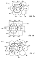
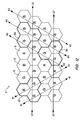
- the sensing layer 3 has subpixels 35 arranged in a hexagonal grid layout 28, shown in heavy outline.
- the hexagonal grid layout 28 results in each of the subpixels 35 in the sensing layer 3 being surrounded by six adjacent subpixels 35.
- the hexagonal grid layout 28 is replicated throughout the sensing layer 3. All seven adjacent subpixels 35 in the hexagonal grid layout 28 are positioned in symmetrical relation to one another. Electrical noise due to differences in distance between adjacent subpixels is minimized by arranging the subpixels 35 in the hexagonal grid layout 28.
- the subpixels 35 have a substantially hexagonal shape.
- the shape of the subpixels 35 can be an equilateral hexagon.
- the sensing layer 3 has subpixels 45 having a substantially circular shape and arranged in the hexagonal grid layout 28.
- the sensing layer 3 has a pixel 30 defined by three of the subpixels 35.
- the subpixels 35 in the pixel 30 are arranged in a triangular configuration 22 as shown in FIG. 5a.
- the triangular configuration 22 when used in conjunction with the hexagonal shape for the subpixels 35 provides for a high density image sensor with symmetry between the subpixels 35 in the pixel 30 and between adjacent pixels 30 in the sensing layer 3.
- the arrangement of the subpixels 35 used to define the pixel 30 is not limited to the triangular configuration 22 and other configurations are possible, such as the subpixels 35 arranged along a line to define the pixels 30, for example.
- the pixel 30 may be defined by three of the subpixels 45. Additionally, the subpixels 45 in the pixel 30 can be arranged in the triangular configuration 22.
- Subpixels can be formed by using photolithography and etching methods common to the semiconductor processing art to create the desired shape for the cavity 6 in the dielectric material of the sensing layer 3.
- the readout cells 20 in row 151 of the readout layer 17 are offset in position with respect to the readout cells 20 in an adjacent row 153 of the readout layer 17 so that the readout cells 20 in the readout layer 17 are also arranged in the hexagonal grid layout 28, shown in heavy outline.
- the hexagonal grid layout 28 is replicated throughout the readout layer 17.
- the readout cells 20 in the readout layer 17 are arranged in the triangular configuration 22 by offsetting the readout cells 20 in the row 151 by a distance of one-half the width of a readout cell 20 with respect the to readout cells 20 in the adjacent row 153.
- the corresponding symmetry in placement between the readout cells 20 in the readout layer 17 and the subpixels 35 in the sensing layer 3, as illustrated in FIG. 5a, allows for flexibility in the relative placement of the subpixels 35 with respect to their matching readout cells 20.
- the subpixels 35 can be positioned directly above their matching readout cells 20, or the subpixels 35 can be positioned above their matching readout cells 20 but displaced in a horizontal direction.
- the opening 8 for the interconnect 21 should be positioned to align with the signal input 24 of its matching readout cells 20. However, alignment is not necessary if intermediate levels of interconnect are used to communicate the output signal from the subpixels 35 to the signal input 24 of the readout cells 20.
- the readout cell 20 includes an amplifier generally designated as 70.
- the output signal from the P-I-N photodiode 7 is communicated to the signal input 24 of the readout cell 20 by the interconnect 21.
- the amplifier 70 is in electrical communication with the signal input 24 and is operative to amplify the output signal.
- the amplifier 70 has an amp output 79 indicative of the amplified output signal.
- the amplifier 70 may include a transistor 93 with a source terminal that provides the amp output 79, a gate terminal connected to a select input 77, and a drain terminal connected to a source terminal of a transistor 91.
- the transistor 91 has a drain terminal connected to a voltage source, such as VDD, for example, and a gate terminal connected to the signal input 24.
- a transistor 95 has a source terminal connected to the signal input 24, a drain terminal connected to a reset voltage input 73, and a gate terminal connected to a reset input 75.
- the transistor 91 amplifies the signal present at the signal input 24.
- the transistor 93 receives the amplified signal from the source terminal of the transistor 91 and transfers the amplified signal to the amp output 79 when the transistor 93 is switched on.
- a voltage present at the reset voltage input 73 is communicated to the gate terminal of transistor 91 when the transistor 95 is switched on by a signal on the reset input 75 and transferred to the amp output 79 when the transistor 93 is switched on.
- the readout layer 17 includes a serpentine bus 89 and a stair-step bus 90.
- the serpentine bus 89 and the stair-step bus 90 are formed on the readout layer 17 and intersect the rows of the readout layer 17.
- the serpentine bus 89 and the stair-step bus 90 can be made from metals such as aluminium and tungsten, for example.
- the serpentine bus 89 and the stair-step bus 90 are operative to route signals between the readout cells 20 and the readout layer 17.
- a row 155 in the readout layer 17 has readout cells 20 with an A-type interconnect pattern 92 formed therein and an adjacent row 157 in the readout layer 17 has readout cells 20 with a B-type interconnect pattern 94 formed therein.
- the readout cells 20 having the A-Type interconnect pattern 92 include a C-shaped interconnect 81 and a first L-shaped interconnect 85.
- the readout cells 20 having the B-type interconnect pattern 94 include a second L-shaped interconnect 83 and a third L-shaped interconnect 87.
- the C-shaped interconnect 81 is in electrical communication with the second L-shaped interconnect 83 and defines the serpentine bus 89.
- the first L-shaped interconnect 85 is in electrical communication with the third L-shaped interconnect 87 defining the stair-step bus 90.
- the serpentine bus 89 and the stair-step bus 90 intersect the row 155 and the adjacent row 157 of the readout layer 17.
- the offset position of the readout cells 20 in the row 155 with respect to the readout cells 20 in the adjacent row 157, coupled with the A-Type interconnect pattern 92 and the B-Type interconnect pattern 94 form an efficient and unique routing structure for communicating signals between the readout cells 20 and the readout plane 17.
- the serpentine bus 89 is in electrical communication with the amp output 79 and the stair-step bus 90 is in electrical communication with the reset voltage input 73.
- the sensing layer 3 has Red subpixels 5R, Green subpixels 5G, and Blue subpixels 5B in an equal distribution RGB colour pattern where the colour of the colour filter is Red for the Red subpixels 5R, Green for the Green subpixels 5G, and Blue for the Blue subpixels 5B.
- the sensing layer 3 can have the subpixels oriented such that any given subpixel is surrounded by adjacent subpixels having a different colour of the colour filter as illustrated by arrows 36.
- the arrows 36 illustrate the Red subpixel 5R surrounded by Green subpixels and Blue subpixels.
- the Green subpixel 5G is surrounded by Red subpixels and Blue subpixels.
- the Blue subpixel 5B is surrounded by Red subpixels and Green subpixels.
- the equal distribution RGB colour pattern is illustrated, the present invention is not limited to the equal distribution RGB colour pattern and other combinations of colors and colour patterns can be used.
- FIG. 8 illustrates the subpixels having a hexagonal shape, the shape of the subpixels can be any non-rectangular shape, for example, the shape of the subpixels can be circular, as noted earlier.
- the sensing layer 3 has Cyan subpixels 5C, Magenta subpixels 5M, and Yellow subpixels 5Y in an equal distribution CMY colour pattern where the colour of the colour filter is Cyan for the Cyan subpixels 5C, Magenta for the Magenta subpixels 5M, and Yellow for the Yellow subpixels 5Y.
- the sensing layer 3 can have the subpixels oriented such that any given subpixel is surrounded by adjacent subpixels having a different colour of the colour filter as illustrated by arrows 36.
- the sensing layer 3 has each subpixel 5 positioned to establish symmetry between adjacent subpixels 5 so that a lineal image traversal in a horizontal direction, as shown by arrows 37, across horizontally adjacent subpixels 5, results in a complete crossing of the subpixels 5 having the equal distribution RGB colour pattern.
- the arrows 37 show that a lineal image traversal in the horizontal direction results in a sequential crossing of the horizontally adjacent subpixels 5 having a colour from the equal distribution RGB colour pattern.
- the arrows 37 show a lineal image traversal in the horizontal direction, if sensing layer 3 is rotated 90 degrees, a vertical lineal image traversal would also make a sequential crossing of vertically adjacent subpixels 5 having the equal distribution RGB colour pattern.
- FIG. 10 illustrates the subpixels 5 having a hexagonal shape
- the shape of the subpixels 5 can be any non-rectangular shape, for example, the shape of the subpixels 5 can be circular.
- the colour pattern for the sensing layer 3 is not limited to the equal distribution RGB colour pattern.
- FIG. 11 illustrates the use of an equal distribution CMY colour pattern for the sensing layer 3.
- the lineal image traversal in the horizontal direction as shown by arrows 37, the lineal image traversal in the first diagonal direction, as shown by arrow 38, and the lineal image traversal in the second diagonal direction, as shown by arrow 40 result in a sequential crossing of adjacent subpixels 5 in their respective lineal directions.
- a pixel 30, shown in heavy outline includes three of the subpixels 5.
- the colour of the colour filter is the same for at least two of the three subpixels 5 in the pixel 30.
- the sensing layer 3 has pixels 30 positioned so that a lineal image traversal in the horizontal direction results in a sequential crossing of horizontally adjacent subpixels 5 having the RGB colour pattern, as shown by arrows 37.
- a lineal image traversal in the vertical direction results in a sequential crossing of vertically adjacent subpixels 5 having the RGB colour pattern if the sensing layer 3 is rotated by 90 degrees.
- a diagonal lineal image traversal in a first direction does not result in a sequential crossing of diagonally adjacent subpixels 5 having the RGB colour pattern. Rather, the arrows 43 show that the traversal in the first direction crosses only the diagonally adjacent subpixels 5 having the same colour of the colour filter.
- This configuration of the pixels 30 and their respective subpixels 5 can be useful in applications such as video, for example, where the output signals from the diagonally adjacent Red subpixels, the diagonally adjacent Green subpixels, and the diagonally adjacent Blue subpixels can be processed as a group to derive RGB data from an image.
- Each arrow 43 is parallel to an adjacent arrow 43 such that the group includes Red, Green, and Blue subpixels in a parallel orientation that form an RGB colour pattern.
- the RGB colour pattern is illustrated, any colour pattern may be used, such as the CMY colour pattern, for example.
- all of the subpixels 5 in the pixels 30 can have the same colour of the colour filter.
- the pixels 30 can be positioned in the sensing layer 3 to implement a variety of application specific colour patterns.
- FIG. 12 illustrates the subpixel 5 having a hexagonal shape, the shape of the subpixel 5 can be any non-rectangular shape, for example, the shape of the subpixel 5 can be circular.
Description
- The present invention relates generally to an active image sensor, for example an active image sensor with an amorphous silicon sensing layer and a semiconductor readout layer.
- Many modern imaging systems such as digital cameras, camcorders, scanners, copiers, and the like require an image sensor capable of capturing an image with high resolution and colour fidelity. A majority of the imaging systems uses a solid-state image sensor due to constraints on system size, weight, power consumption, heat dissipation, and durability. The ability of the imaging system to capture images with high resolution and colour fidelity depends to a large extent on the image sensor used. Image sensor resolution is typically measured in number of pixels contained in the image sensor.
The resolution of a solid-state sensor can be increased by shrinking the size of the pixels so that more pixels fit within a predetermined area. An image incident on an image sensor having more pixels per unit of area can be captured with greater resolution than an image sensor having fewer pixels per unit of area. Pixel geometry and symmetry between pixels can also affect the number of pixels per unit of area. Additionally, the symmetry between pixels can affect colour aliasing. Other factors, such as electrical noise generated by the pixels can affect image quality. Additionally, for colour images, the colour fidelity of the image can be affected by a predetermined colour pattern assigned to the pixels in the image sensor. - Desirable attributes of an image sensor include low electrical noise, flexibility in colour pattern, optimized pixel density and geometry for increased resolution, symmetry between adjacent pixels, and maximized pixel fill-factor. Low electrical noise prevents an image signal generated by the pixel from being corrupted by noise; furthermore, noise and leakage current from an individual pixel can affect the image signal from adjacent pixels. Additionally, pixel electrical noise can be affected by pixel geometry and symmetry between pixels. Circuitry or algorithms to filter out the electrical noise can be minimized or eliminated by reducing the noise generated by each pixel. A flexible colour pattern allows the image sensor to be tailored to specific applications such as a RGB colour pattern for photography or video, or a CMY colour pattern for printing or scanning, for example.
- Pixels having a rectangular geometry can generate additional noise due to abrupt rectangle edges which create leakage current in an active device such as a photodiode, for example. A pixel geometry that eliminates noise due to abrupt edges is desirable. Further, it is desirable to maximise the active area of the pixel devoted to capturing the image so that the ratio of the active area to the pixel area approaches a fill-factor of 100%. By removing components, such as transistors and signal routing lines, from the pixel, the area that was occupied by the components can be used to maximise the active area of the pixel thereby increasing the fill-factor.
- Previous image sensor designs include photo-gate active pixel sensors, bulk silicon photodiode pixel sensors with three transistors, pulsed bipolar CMOS active pixel sensors, and rectangular CMOS pixel sensors.
- The photo-gate active pixel sensor utilises four transistors inside of a CMOS photo-gate pixel for low noise operation and for electronic shuttering. However, this number of transistors results in a pixel area that is not competitive with state-of-the-art CCD image sensors that have pixel areas approaching 5 x 5µm2. The number of transistors in the photo-gate sensor results in a lower fill-factor when compared to the state-of-the-art CCD image sensor.
- The pulsed bipolar CMOS active pixel sensor employs a vertical bipolar device in a CMOS process. The use of bipolar devices results in a smaller pixel area due to fewer transistors in the pixel; however, disadvantages of this design include image lag and the need to amplify an output signal from the pixel with a high β gain bipolar transistor. The high β gain bipolar transistor exhibits signal degradation under low current conditions and limits scalability of the pixel due to an integrating amplification stage in a readout path of the pixel. Further, an extra emitter terminal is required to prevent an overflow condition. The extra emitter terminal creates an unsymmetrical pixel layout in the CMOS process. In the pulsed bipolar CMOS active pixel sensor, pixel area is not minimized because CMOS design rules require adjacent pixels to be spaced apart to comply with design rules for N-well spacing.
- The bulk silicon photodiode pixel sensor is not competitive with the state-of the-art CCD image sensor because the photodiode and the transistors are integral to the same silicon layer and the area occupied by the transistors reduces the active area available for the photodiode resulting in a fill-factor of about 30% using 1.2µm CMOS process technology.
- Rectangular CMOS active pixel sensor designs utilise a rectangular pixel geometry with the pixels laid out in a rectangular grid. It is clearly understood that the rectangular grid does not result in an optimized pixel density. Bayer's colour pattern was developed as the colour filter array (CFA) pattern for the rectangular grid. In the Bayer CFA pattern, colour density for Red, Green, and Blue sensors is in the ratio of 1:2:1. Therefore, there are two Green pixels for each Red pixel and Blue pixel in the array. In general, the colour density for the Bayer CFA pattern is not the best choice because it undersamples two of the sensor colors (Red and Blue) and the colour pattern kernel is not symmetric. In the Bayer CFA pattern, linear horizontal, linear vertical, and linear diagonal image features never pass through more than two different colour sensor locations because the Red and the Blue sensor locations are never adjacent to sensors of the same colour. The rectangular pixel geometry is not amenable to flexible colour patterning.
- In FIG. 1, there is provided for purposes of illustration a prior art rectangular CMOS active pixel sensor designated generally as 100. The
sensor 100 has a plurality ofsubpixels 101. Four of thesubpixels 101 define apixel 103, shown in heavy outline. Thepixel 103 has twoGreen subpixels 105, oneRed subpixel 107, and oneBlue subpixel 109. This arrangement of the colour pattern for thesubpixels 101 in thepixel 103 corresponds to the Bayer CFA pattern wherein the colour density of the Redsubpixel 107, the Greensubpixels 105, and theBlue subpixel 109 is in the ratio of 1:2:1, wherein thepixel 103 has twoGreen subpixels 105 for oneRed subpixel 107 and oneBlue sub pixel 109. - FIG. 2 illustrates lineal image feature traversals across
prior art sensor 100. In a first horizontal traverse as shown by anarrow 133, the image feature traverses theGreen subpixels 105 and theRed subpixels 107. In a second horizontal traverse as shown by anarrow 122, the image feature traverses theBlue subpixels 109 and theGreen subpixels 105. The firsthorizontal traverse 133 never crosses theBlue subpixels 109. Similarly, the secondhorizontal traverse 122 never crosses theRed subpixels 107. Because the Bayer CFA colour pattern kernel is not symmetric, the firsthorizontal traverse 133 and the secondhorizontal traverse 122 never make a sequential crossing of the Redsubpixels 107, the Greensubpixels 105, and theBlue subpixels 109 in a single traverse of thesensor 100. The same is true for a first vertical traverse as shown by anarrow 135 where only theGreen subpixels 105 and theRed subpixels 107 are traversed. In a second vertical traverse as shown by anarrow 124, only theGreen subpixels 105 and theBlue subpixels 109 are traversed. Additionally, in a first diagonal traverse as shown by anarrow 137, only all theGreen subpixels 105 are traversed. In a second diagonal traverse as shown by anarrow 126 only theRed subpixels 107 and theBlue subpixels 109 are traversed. Because the Bayer CFA pattern lacks colour symmetry betweenadjacent subpixels 101, a sequential traverse of the Redsubpixels 107, the Greensubpixels 105, and theBlue subpixels 109 consistent with the RGB colour pattern is not possible for vertical, horizontal, and diagonal image features. - CMOS photo-gate and photodiode implementations of an active pixel sensor exhibit crosstalk between pixels of different colour due to electron leakage from an electron collection node. Additionally, crosstalk is exacerbated by any non-uniformity in distance between pixels. Such non-uniformity can result in a non-uniform crosstalk pattern especially for different colour channels. Due to the rectangular geometry and the Bayer CFA pattern, a pixel is surrounded by a group of eight pixels. The pixels in the group that are horizontally or vertically adjacent to the surrounded pixel are closer to the surrounded pixel than pixels that are diagonally adjacent to the surrounded pixel resulting in a variation in distance between the surrounded pixel and the other pixels in the group. A non-uniform crosstalk pattern is created by the variation in distance.
- In FIG. 3, for purposes of illustration, the relative distance between
adjacent subpixels 101 ofprior art sensor 100 is shown byarrows 139.Red subpixel 117 is surrounded by fourGreen subpixels 125 and fourBlue subpixels 129. TheBlue subpixels 129 are diagonally adjacent to theRed subpixel 117 and are at a greater distance from theRed subpixel 117 than theGreen subpixels 125 that are abutted to theRed subpixel 117. Similarly,Blue subpixel 119 is surrounded by fourGreen subpixels 125 and fourRed subpixels 127 with theRed subpixels 127 positioned diagonal to and at a greater distance from theBlue subpixel 119 than theGreen subpixels 125. The Green subpixels 125 are abutted to theBlue subpixel 119 and are therefore closer in distance to theBlue subpixel 119 than the Red subpixels 127. Green subpixel 115 is surrounded by twoRed subpixels 127, twoBlue subpixels 129, and fourGreen subpixels 125. The twoRed subpixels 127 and the twoBlue subpixels 129 are abutted to the Green subpixel 115, whereas the fourGreen subpixels 125 are positioned diagonal to the Green subpixel 115. Because of the oversampling of Green by a factor of two to one over Red and Blue in the Bayer CFA pattern, the Green subpixel 115 is surrounded by fourGreen subpixels 125. For each instance of a surrounded subpixel the extra distance between the surrounded pixel and diagonally adjacent pixels can result in a non-uniform cross talk pattern. For the Green subpixel 115, the non-uniform cross talk pattern can be exacerbated because the Green subpixel 115 is not surrounded by an equal number of subpixels having the same colour. The twoBlue subpixels 129 and the twoRed subpixels 127 may not have cross talk patterns that cancel, resulting in additional cross talk due to colour imbalance that is additive with the cross talk due to the extra distance of the fourGreen subpixels 125 that are diagonal to the Green subpixel 115. - US 5,619,033 discloses a photodetecting device with at least one photodiode formed over and coupled to a transistor. The photodetecting devices are formed in a matrix. Each photodiode is separated from adjacent photodiodes by notches which may be formed in any two dimensional polygonal pattern such as triangular or hexagonal patterns.
- From the foregoing it will be apparent that there is a need for a high resolution, low noise, flexible colour pattern, high fill-factor, optimized pixel geometry, high density, and low crosstalk active image sensor.
- The present invention seeks to provide an improved image sensor.
- According to an aspect of the present invention, there is provided an image sensor as specified in claim 1.
- In a preferred embodiment, there is provided an active image sensor in which photodiodes are laid out in a geometrically-efficient pattern, preferably hexagonal as opposed to rectilinear, and in which the photodiodes and their associated amplifiers are stacked vertically. Such an image sensor has a higher pixel density than the other sensors and offers higher resolution, better colour fidelity, less noise, less crosstalk, and a more flexible CFA pattern.
- The image sensor includes a semiconductor substrate having a plurality of readout cells formed in the substrate. The substrate defines a readout layer with the readout cells positioned in rows. Each readout cell has a signal input. A dielectric material is formed on the readout layer to define a sensing layer. A plurality of cavities are formed in the sensing layer. The cavities are arranged in a hexagonal grid layout and are positioned in opposing relation to the readout cells in the readout layer. An amorphous silicon P-I-N photodiode is formed in each cavity of the sensing layer. Each photodiode generates an output signal indicative of light incident on the photodiode. An interconnect communicates the output signal from the photodiode to the signal input of the readout cell. A biased optically transparent electrode is disposed in each cavity and operates to bias the photodiode and allows light incident on the electrode to be imaged onto the photodiode. The photodiode and the electrode define a subpixel of the sensing layer. An amplifier is disposed in each readout cell vertically stacked beneath an associated photodiode and in electrical communication therewith to amplify the signal from that photodiode. Placing the amplifier beneath its associated photodiode eliminates signal routing lines, transistors, and other components from the active area of the photodiode thereby maximising the area of the photodiode available for receiving incident light.
- An opaque optical shield may be used to prevent light incident on the photodiode from impinging on the readout layer.
- The subpixel is preferably shaped so as to optimise subpixel density in the sensing layer. A hexagonal shape works well, but another suitable shape such as a circular shape may be used.
- In one embodiment, the readout layer has a serpentine bus and a stair-step bus. The serpentine bus and the stair-step bus are defined by a row having a first pattern of signal routing and an adjacent row having a second pattern of signal routing. The first and second patterns align to form the serpentine bus and the stair-step bus. The serpentine bus and the stair-step bus are extended throughout the readout layer. As mentioned above, the active area of the photodiode in the sensing layer is maximized by placing the signal routing in the readout layer.
- The sensing layer may include a filter layer positioned adjacent to the electrode. In one embodiment the filter layer is a colour filter. The colour filter may be varied among the subpixels to produce a desired colour pattern or to create symmetry or asymmetry in the colour filter pattern among adjacent subpixels.
- The sensing layer may include an infrared filter to attenuate the absorption of infrared noise from the light incident on the subpixel.
- In another embodiment, the sensing layer includes a microlens positioned adjacent the subpixel for focusing incident light onto the subpixel.
- An embodiment of the present invention is described below, by way of example only, with reference to the accompanying drawings, in which:
- FIG. 1 is a top plan view of a prior art rectangular CMOS active pixel sensor with a Bayer CFA pattern.
- FIG. 2 is a top plan view of a prior art rectangular CMOS active pixel sensor illustrating lineal image traversals.
- FIG. 3 is a top plan view of a prior art rectangular CMOS active pixel sensor illustrating relative distance between adjacent subpixels.
- FIG. 4 is a cross-sectional view of an embodiment of image sensor with a sensing layer and a rectangular readout layer.
- FIG. 5a is a top plan view of an embodiment of image sensor with hexagonally shaped subpixels.
- FIG. 5b is a top plan view of an embodiment image sensor with readout cells in a hexagonal grid layout.
- FIG. 6 is a top plan view of an embodiment of image sensor with circularly shaped subpixels.
- FIG. 7a is a schematic of an embodiment of amplifier in a readout cell.
- FIG. 7b is a top plan view of an embodiment of readout cell signal routing.
- FIG. 8 is a top plan view of an embodiment of image sensor with an equal distribution RGB colour patter.
- FIG. 9 is a top plan view of an embodiment of circular array with an equal distribution OMY colour pattern.
- FIG. 10 is a top plan view of an embodiment of image sensor showing lineal image traversals of the RGB colour pattern.
- FIG. 11 is a top plan view of an embodiment of image sensor showing lineal image traversals of the CMY colour pattern.
- FIG. 12 is a top plan view of an embodiment of image sensor showing lineal image traversals of a colour pattern.
- As shown in the drawings for purposes of illustration, the preferred embodiment is an image sensor including a semiconductor substrate defining a readout layer and a dielectric material defining a sensing layer. The readout layer has a plurality of readout cells formed in the substrate an arranged in rows. The readout cells in a row are offset in position with respect to the readout cells in an adjacent row. Each readout cell has a signal input. The dielectric material is formed on the readout layer to define the sensing layer. A plurality of cavities are formed in the sensing layer. The cavities are arranged in a hexagonal grid layout and are positioned in opposing relation to the readout cells in the readout layer. A portion of each cavity has an opening in communication with the signal input of the readout cell. An amorphous silicon P-I-N photodiode is formed in each cavity and defines a subpixel of the image sensor. Each photodiode generates an output signal indicative of light incident thereon. An interconnect positioned in the opening of each cavity communicates the output signal from the photodiode to the signal input of the readout cell. A biased optically transparent electrode is disposed in the cavity and operates to bias the photodiode and allows light incident on the electrode to be imaged onto the photodiode. The photodiode and the electrode define a subpixel. The image sensor has an optimal subpixel density, maximises subpixel fill-factor, has a flexible subpixel geometry, can be implemented with a variety of colour patterns, reduces electrical noise and crosstalk, and provides for uniform spacing and symmetry between subpixels.
- Referring to FIG.4, there is shown an embodiment of image sensor which includes a semiconductor substrate that defines a
readout layer 17. Thereadout layer 17 has a plurality ofreadout cells 20 formed therein. FIG. 4 illustrates onereadout cell 20 in thereadout layer 17. Thereadout cells 20 are arranged in rows with thereadout cells 20 in a row offset in position with respect to thereadout cells 20 in an adjacent row. Thereadout layer 17 can be any semiconductor substrate, for example, bulk silicon. - A dielectric material is formed on the
readout layer 17 to define asensing layer 3. A plurality ofcavities 6 are formed in thesensing layer 3. Thecavities 6 are arranged in a hexagonal grid layout and are positioned in opposing relation to thereadout cells 20 so that there is a one-to-one correspondence between eachcavity 6 in thesensing layer 3 and eachreadout cell 20 in thereadout layer 17. The dielectric material can be any insulator such as silicon dioxide or silicon nitride, for example. - An amorphous
silicon P-I-N photodiode 7 is formed in thecavity 6. Thephotodiode 7 is operative to generate an output signal indicative of light incident on thephotodiode 7. Thephotodiode 7 can be formed by depositing a layer of N-typeamorphous silicon 15 in thecavity 6 followed by a layer of intrinsicamorphous silicon 13, and finally a layer of P-typeamorphous silicon 11, for example. A portion of thecavity 6 has anopening 8 in communication with asignal input 24 of thereadout cell 20. Aninterconnect 21 disposed in theopening 8 communicates the output signal of thephotodiode 7 to thesignal input 24. Theinterconnect 21 can be made from a conductor such as aluminium or tungsten, for example. - A biased optically
transparent electrode 9 is disposed on thephotodiode 7 to bias thephotodiode 7 and to allow light incident on theelectrode 9 to be imaged onto thephotodiode 7. Theelectrode 9 is in electrical communication with a voltage source such as ground and with thelayer 11. Theelectrode 9 can be implemented using indium tin oxide (ITO), for example. Theelectrode 9 and thephotodiode 7 define asubpixel 5 of the image sensor 1. Fig. 4 illustrates onesubpixel 5 in thesensing layer 3. - In an embodiment of the present invention, the
sensing layer 3 may include afilter layer 25 operative to pass a selected wavelength of light from the light incident on thesubpixel 5. Thefilter layer 25 is shown adjacent to theelectrode 9; however, thefilter layer 25 can be positioned anywhere in thesensing layer 3 provided that the incident light is filtered before reaching thesubpixel 5. - In one embodiment, the
filter layer 25 is a colour filter. The colour filter has a predetermined colour. The wavelength of light passed by the colour filter can be a colour such as Red, Green, Blue, Cyan, Magenta, or Yellow, for example. Any colour suitable for the desired application of the image sensor 1 may be used for the colour of the colour filter. In some applications, particularly those involving digital photography or video, the colour of the colour filter can be a colour from a RGB colour pattern consisting of Red, Green, and Blue, for example. For printing or scanning applications, the colour of the colour filter can be a colour from a CMY colour pattern consisting of Cyan, Magenta, and Yellow, for example. - Additionally, the
sensing layer 3 may include aninfrared filter 27 positioned adjacent theelectrode 9. Theinfrared filter 27 is operative to attenuate infrared noise from the light incident on thesubpixel 5. A separateinfrared filter 27 may be positioned adjacent to each of thesubpixels 5 as shown in FIG. 4 or theinfrared filter 27 may be a single layer that covers all of thesubpixels 5 in thesensing layer 3. - In another embodiment of the present invention, the
sensing layer 3 includes amicrolens 29 positioned to focus incident light onto thesubpixel 5. Themicrolens 29 can be implemented using state-of-the-art semiconductor microlens fabrication techniques. - In one embodiment of the present invention, the
subpixel 5 includes an opaqueoptical shield layer 23. Theshield layer 23 is operative to prevent light incident on thesubpixel 5 from passing through thesensing layer 3 and impinging on thereadout layer 17. A seconddielectric material 2 may be deposited above theshield layer 23 to electrically isolate theshield layer 23 from thelayer 15. In another embodiment the opaqueoptical shield layer 23 is disposed in thesensing layer 3 intermediate between thesubpixel 5 and thereadout layer 17. - Referring to FIG. 5a, the
sensing layer 3 hassubpixels 35 arranged in ahexagonal grid layout 28, shown in heavy outline. Thehexagonal grid layout 28 results in each of the subpixels 35 in thesensing layer 3 being surrounded by sixadjacent subpixels 35. Thehexagonal grid layout 28 is replicated throughout thesensing layer 3. All sevenadjacent subpixels 35 in thehexagonal grid layout 28 are positioned in symmetrical relation to one another. Electrical noise due to differences in distance between adjacent subpixels is minimized by arranging the subpixels 35 in thehexagonal grid layout 28. In one embodiment of the present invention, thesubpixels 35 have a substantially hexagonal shape. Preferably, the shape of the subpixels 35 can be an equilateral hexagon. Similarly, in another embodiment of the present invention, as illustrated in FIG. 6, thesensing layer 3 hassubpixels 45 having a substantially circular shape and arranged in thehexagonal grid layout 28. - In another embodiment of the present invention, the
sensing layer 3 has apixel 30 defined by three of thesubpixels 35.
In one embodiment of the present invention, thesubpixels 35 in thepixel 30 are arranged in atriangular configuration 22 as shown in FIG. 5a. Thetriangular configuration 22 when used in conjunction with the hexagonal shape for thesubpixels 35 provides for a high density image sensor with symmetry between the subpixels 35 in thepixel 30 and betweenadjacent pixels 30 in thesensing layer 3. The arrangement of the subpixels 35 used to define thepixel 30 is not limited to thetriangular configuration 22 and other configurations are possible, such as the subpixels 35 arranged along a line to define thepixels 30, for example. Similarly, in another embodiment of the present invention, as illustrated in FIG. 6, thepixel 30 may be defined by three of thesubpixels 45. Additionally, thesubpixels 45 in thepixel 30 can be arranged in thetriangular configuration 22. - Subpixels can be formed by using photolithography and etching methods common to the semiconductor processing art to create the desired shape for the
cavity 6 in the dielectric material of thesensing layer 3. - In one embodiment of the present invention, as illustrated in FIG. 5b, the
readout cells 20 inrow 151 of thereadout layer 17 are offset in position with respect to thereadout cells 20 in anadjacent row 153 of thereadout layer 17 so that thereadout cells 20 in thereadout layer 17 are also arranged in thehexagonal grid layout 28, shown in heavy outline. Thehexagonal grid layout 28 is replicated throughout thereadout layer 17. - In another embodiment, the
readout cells 20 in thereadout layer 17 are arranged in thetriangular configuration 22 by offsetting thereadout cells 20 in therow 151 by a distance of one-half the width of areadout cell 20 with respect the to readoutcells 20 in theadjacent row 153. The corresponding symmetry in placement between thereadout cells 20 in thereadout layer 17 and the subpixels 35 in thesensing layer 3, as illustrated in FIG. 5a, allows for flexibility in the relative placement of the subpixels 35 with respect to theirmatching readout cells 20. For example, thesubpixels 35 can be positioned directly above theirmatching readout cells 20, or the subpixels 35 can be positioned above theirmatching readout cells 20 but displaced in a horizontal direction. If thesubpixels 35 are displaced, theopening 8 for theinterconnect 21 should be positioned to align with thesignal input 24 of itsmatching readout cells 20. However, alignment is not necessary if intermediate levels of interconnect are used to communicate the output signal from thesubpixels 35 to thesignal input 24 of thereadout cells 20. - According to the invention, as illustrated in FIG. 7a, the
readout cell 20 includes an amplifier generally designated as 70. The output signal from theP-I-N photodiode 7 is communicated to thesignal input 24 of thereadout cell 20 by theinterconnect 21. Theamplifier 70 is in electrical communication with thesignal input 24 and is operative to amplify the output signal. Theamplifier 70 has anamp output 79 indicative of the amplified output signal. - The
amplifier 70 may include atransistor 93 with a source terminal that provides theamp output 79, a gate terminal connected to aselect input 77, and a drain terminal connected to a source terminal of atransistor 91. Thetransistor 91 has a drain terminal connected to a voltage source, such as VDD, for example, and a gate terminal connected to thesignal input 24. Atransistor 95 has a source terminal connected to thesignal input 24, a drain terminal connected to areset voltage input 73, and a gate terminal connected to areset input 75. Thetransistor 91 amplifies the signal present at thesignal input 24. Thetransistor 93 receives the amplified signal from the source terminal of thetransistor 91 and transfers the amplified signal to theamp output 79 when thetransistor 93 is switched on. A voltage present at thereset voltage input 73 is communicated to the gate terminal oftransistor 91 when thetransistor 95 is switched on by a signal on thereset input 75 and transferred to theamp output 79 when thetransistor 93 is switched on. - In an embodiment of the present invention, as illustrated in FIG. 7b, the
readout layer 17 includes aserpentine bus 89 and a stair-step bus 90. Theserpentine bus 89 and the stair-step bus 90 are formed on thereadout layer 17 and intersect the rows of thereadout layer 17. Theserpentine bus 89 and the stair-step bus 90 can be made from metals such as aluminium and tungsten, for example. Theserpentine bus 89 and the stair-step bus 90 are operative to route signals between thereadout cells 20 and thereadout layer 17. - In one embodiment of the present invention, a
row 155 in thereadout layer 17 hasreadout cells 20 with anA-type interconnect pattern 92 formed therein and anadjacent row 157 in thereadout layer 17 hasreadout cells 20 with a B-type interconnect pattern 94 formed therein. Thereadout cells 20 having theA-Type interconnect pattern 92, include a C-shapedinterconnect 81 and a first L-shapedinterconnect 85. Thereadout cells 20 having the B-type interconnect pattern 94 include a second L-shapedinterconnect 83 and a third L-shapedinterconnect 87. The C-shapedinterconnect 81 is in electrical communication with the second L-shapedinterconnect 83 and defines theserpentine bus 89. The first L-shapedinterconnect 85 is in electrical communication with the third L-shapedinterconnect 87 defining the stair-step bus 90. Theserpentine bus 89 and the stair-step bus 90 intersect therow 155 and theadjacent row 157 of thereadout layer 17. - The offset position of the
readout cells 20 in therow 155 with respect to thereadout cells 20 in theadjacent row 157, coupled with theA-Type interconnect pattern 92 and the B-Type interconnect pattern 94 form an efficient and unique routing structure for communicating signals between thereadout cells 20 and thereadout plane 17. - In another embodiment of the present invention, the
serpentine bus 89 is in electrical communication with theamp output 79 and the stair-step bus 90 is in electrical communication with thereset voltage input 73. - In one embodiment of the present invention, as illustrated in FIG. 8, the
sensing layer 3 hasRed subpixels 5R,Green subpixels 5G, andBlue subpixels 5B in an equal distribution RGB colour pattern where the colour of the colour filter is Red for theRed subpixels 5R, Green for theGreen subpixels 5G, and Blue for theBlue subpixels 5B. Thesensing layer 3 can have the subpixels oriented such that any given subpixel is surrounded by adjacent subpixels having a different colour of the colour filter as illustrated byarrows 36. Thearrows 36, illustrate theRed subpixel 5R surrounded by Green subpixels and Blue subpixels. TheGreen subpixel 5G is surrounded by Red subpixels and Blue subpixels. TheBlue subpixel 5B is surrounded by Red subpixels and Green subpixels. Although the equal distribution RGB colour pattern is illustrated, the present invention is not limited to the equal distribution RGB colour pattern and other combinations of colors and colour patterns can be used. Although FIG. 8 illustrates the subpixels having a hexagonal shape, the shape of the subpixels can be any non-rectangular shape, for example, the shape of the subpixels can be circular, as noted earlier. - In one embodiment of the present invention, as illustrated in FIG. 9, the
sensing layer 3 hasCyan subpixels 5C,Magenta subpixels 5M, andYellow subpixels 5Y in an equal distribution CMY colour pattern where the colour of the colour filter is Cyan for the Cyan subpixels 5C, Magenta for theMagenta subpixels 5M, and Yellow for theYellow subpixels 5Y. As noted above, thesensing layer 3 can have the subpixels oriented such that any given subpixel is surrounded by adjacent subpixels having a different colour of the colour filter as illustrated byarrows 36. - In another embodiment of the present invention, as illustrated in FIG. 10, the
sensing layer 3 has eachsubpixel 5 positioned to establish symmetry betweenadjacent subpixels 5 so that a lineal image traversal in a horizontal direction, as shown byarrows 37, across horizontallyadjacent subpixels 5, results in a complete crossing of thesubpixels 5 having the equal distribution RGB colour pattern. Thearrows 37 show that a lineal image traversal in the horizontal direction results in a sequential crossing of the horizontallyadjacent subpixels 5 having a colour from the equal distribution RGB colour pattern. Although thearrows 37 show a lineal image traversal in the horizontal direction, ifsensing layer 3 is rotated 90 degrees, a vertical lineal image traversal would also make a sequential crossing of verticallyadjacent subpixels 5 having the equal distribution RGB colour pattern. - A lineal image traversal in a first diagonal direction, as shown by
arrows 38, across diagonallyadjacent subpixels 5 in thesensing layer 3, results in a complete crossing of the diagonallyadjacent subpixels 5 having the equal distribution RGB colour pattern. Similarly, a lineal image traversal in a second diagonal direction, as shown byarrows 40, of diagonallyadjacent subpixels 5, results in a complete crossing of the diagonallyadjacent subpixels 5 having the equal distribution RGB colour pattern. Although FIG. 10 illustrates thesubpixels 5 having a hexagonal shape, the shape of thesubpixels 5 can be any non-rectangular shape, for example, the shape of thesubpixels 5 can be circular. Further, the colour pattern for thesensing layer 3 is not limited to the equal distribution RGB colour pattern. - FIG. 11 illustrates the use of an equal distribution CMY colour pattern for the
sensing layer 3. As noted above, the lineal image traversal in the horizontal direction as shown byarrows 37, the lineal image traversal in the first diagonal direction, as shown byarrow 38, and the lineal image traversal in the second diagonal direction, as shown byarrow 40, result in a sequential crossing ofadjacent subpixels 5 in their respective lineal directions. - In another embodiment of the present invention, as illustrated in FIG. 12, a
pixel 30, shown in heavy outline, includes three of thesubpixels 5. The colour of the colour filter is the same for at least two of the threesubpixels 5 in thepixel 30. Thesensing layer 3 haspixels 30 positioned so that a lineal image traversal in the horizontal direction results in a sequential crossing of horizontallyadjacent subpixels 5 having the RGB colour pattern, as shown byarrows 37. Similarly, a lineal image traversal in the vertical direction results in a sequential crossing of verticallyadjacent subpixels 5 having the RGB colour pattern if thesensing layer 3 is rotated by 90 degrees. - A diagonal lineal image traversal in a first direction, as shown by
arrows 43, does not result in a sequential crossing of diagonallyadjacent subpixels 5 having the RGB colour pattern. Rather, thearrows 43 show that the traversal in the first direction crosses only the diagonallyadjacent subpixels 5 having the same colour of the colour filter. This configuration of thepixels 30 and theirrespective subpixels 5 can be useful in applications such as video, for example, where the output signals from the diagonally adjacent Red subpixels, the diagonally adjacent Green subpixels, and the diagonally adjacent Blue subpixels can be processed as a group to derive RGB data from an image. Eacharrow 43 is parallel to anadjacent arrow 43 such that the group includes Red, Green, and Blue subpixels in a parallel orientation that form an RGB colour pattern. - On the other hand, a diagonal lineal image traversal in a second direction, as shown by
arrows 41, results in a sequential crossing of diagonallyadjacent subpixels 5 having the RGB colour pattern. Although the RGB colour pattern is illustrated, any colour pattern may be used, such as the CMY colour pattern, for example. Optionally, all of thesubpixels 5 in thepixels 30 can have the same colour of the colour filter. Thepixels 30 can be positioned in thesensing layer 3 to implement a variety of application specific colour patterns. Although FIG. 12 illustrates thesubpixel 5 having a hexagonal shape, the shape of thesubpixel 5 can be any non-rectangular shape, for example, the shape of thesubpixel 5 can be circular.
Claims (10)
- An image sensor, comprising:a semiconductor substrate providing a readout layer (17) which includes a plurality of readout cells (20) formed therein disposed in rows, each row having readout cells (20) offset in position with respect to the readout cells in an adjacent row;a dielectric material formed on the readout layer (17) which has formed therein a plurality of cavities (6) arranged in a hexagonal grid layout and positioned in one-to-one correspondence with the readout cells, a portion of each of the cavities including an opening in communication with a signal input (24) of one of the readout cells;a sensing layer (3) comprising an amorphous silicon PIN photodiode (7) disposed in each cavity and operable to generate an output signal indicative of light incident on that PIN photodiode;an interconnect (21) disposed in the opening of each cavity and operable to communicate electrically the output signal from the PIN photodiode to the signal input (24) of the readout cell;a biased optically transparent electrode (9) disposed on the PIN photodiode and operable to bias the PIN photodiode and to allow light incident on the electrode to be imaged onto the PIN photodiode; characterised in thatan amplifier (70) is disposed in each readout cell in electrical communication with the signal input (24) and including an amp output (79) at which an amplified version of the output signal is provided;wherein each PIN photodiode and transparent electrode together define a subpixel(5).
- A sensor as in claim 1, wherein the shape of the subpixels (5) is hexagonal, equilaterally hexagonal, or circular.
- A sensor as in claim 1 or 2, wherein each subpixel (5) includes an opaque optical shield layer (23) operable to prevent light incident on the PIN photodiode from impinging on the readout layer (17).
- A sensor as in claim 1, 2 or 3, wherein three subpixels or three readout cells are arranged in a triangular configuration to define a pixel (30).
- A sensor as in any one of the preceding claims, wherein the amplifier comprises:a select input (77) operable to enable the amp output, whereby the amplified output signal communicates with the amp output when the select input is enabled;a terminal in communication with a reset voltage (75); anda reset input (73) operable to set the amp output to the reset voltage.
- A sensor as in claim 5, wherein the readout layer (17) comprises:a serpentine bus (89) formed on the readout layer (17) and intersecting the rows of the readout layer; anda stair-step bus (90) formed on the readout layer (17) and intersecting the rows of the readout layer, the serpentine bus and the stair-step bus being operable to communicate signals between the readout cells and the readout layer.
- A sensor as in claim 6, wherein the rows of the readout layer comprise:a first type interconnect pattern (92) formed on the readout cells of a first row, including a C-shaped interconnect (81) and a first L-shaped interconnect (85); anda second type interconnect pattern (94) formed on the readout cells of a second row adjacent to the first row, including a second L-shaped interconnect (83) and a third L-shaped interconnect (87);wherein the C-shaped interconnect (81) is in electrical communication with the second L-shaped interconnect (83) providing the serpentine bus (89), and the first L-shaped interconnect (85) is in electrical communication with the third L-shaped interconnect (87) providing the stair-step bus (90).
- A sensor as in claim 7, wherein the serpentine bus (89) is in electrical communication with the amp output and the stair step bus (90) is in electrical communication with the reset voltage.
- A sensor as in any preceding claim, wherein the sensing layer (3) comprises:an infrared filter (27) positioned adjacent the electrode (9) and operable to attenuate the absorption of infrared noise from the light incident on the subpixel; and/ora microlens (29) disposed adjacent the subpixel (5) and operable to focus incident light onto the subpixel.
- A sensor as in any preceding claim, wherein the sensing layer comprises; a filter layer (25) positioned adjacent the electrode (9) and operable to pass a selected wavelength of light from the light incident on the subpixel; the sensor preferably including one or more of the following features:(a) the filter layer is a colour filter having a predetermined colour;(b) three subpixels (5) form a pixel and the colour of the filter is the same for at least two of the subpixels in the pixel;(c) the wavelength of the filter for any given subpixel is different from the wavelength of the filter of any adjacent subpixel;(d) the colour of the filter is selected from the group consisting of red, green, blue, cyan, magenta, and yellow;(e) the colours of the filters for adjacent subpixels define an equal distribution RGB colour pattern and the colors of the filters are selected from the group consisting of red, green, and blue;(f) the colours of the filters for adjacent subpixels define an equal distribution CMY colour pattern and the colors of the filters are selected from the group consisting of cyan, magenta, and yellow; and(g) the subpixels are positioned so that a lineal image traversal through adjacent subpixels results in a sequential crossing of the subpixels having a RGB or CMY colour pattern.
Applications Claiming Priority (2)
| Application Number | Priority Date | Filing Date | Title |
|---|---|---|---|
| US09/243,186 US6252218B1 (en) | 1999-02-02 | 1999-02-02 | Amorphous silicon active pixel sensor with rectangular readout layer in a hexagonal grid layout |
| US243186 | 1999-02-02 |
Publications (3)
| Publication Number | Publication Date |
|---|---|
| EP1026747A2 EP1026747A2 (en) | 2000-08-09 |
| EP1026747A3 EP1026747A3 (en) | 2001-08-16 |
| EP1026747B1 true EP1026747B1 (en) | 2006-11-02 |
Family
ID=22917678
Family Applications (1)
| Application Number | Title | Priority Date | Filing Date |
|---|---|---|---|
| EP00300516A Expired - Lifetime EP1026747B1 (en) | 1999-02-02 | 2000-01-25 | Image sensor |
Country Status (4)
| Country | Link |
|---|---|
| US (1) | US6252218B1 (en) |
| EP (1) | EP1026747B1 (en) |
| JP (1) | JP4366702B2 (en) |
| DE (1) | DE60031590T2 (en) |
Families Citing this family (74)
| Publication number | Priority date | Publication date | Assignee | Title |
|---|---|---|---|---|
| US7012645B1 (en) * | 1999-08-26 | 2006-03-14 | Micron Technology, Inc. | Image sensor with p-type circuitry and n-type photosensor |
| TW451447B (en) * | 1999-12-31 | 2001-08-21 | Samsung Electronics Co Ltd | Contact structures of wirings and methods for manufacturing the same, and thin film transistor array panels including the same and methods for manufacturing the same |
| US6563101B1 (en) * | 2000-01-19 | 2003-05-13 | Barclay J. Tullis | Non-rectilinear sensor arrays for tracking an image |
| US6536907B1 (en) * | 2000-02-08 | 2003-03-25 | Hewlett-Packard Development Company, L.P. | Aberration compensation in image projection displays |
| US7154546B1 (en) * | 2000-08-07 | 2006-12-26 | Micron Technology, Inc. | Pixel optimization for color |
| US20040113220A1 (en) * | 2000-12-21 | 2004-06-17 | Peter Rieve | Optoelectronic component for conversion electromagnetic radiation into an intensity-dependent photocurrent |
| US8103877B2 (en) * | 2000-12-21 | 2012-01-24 | Digimarc Corporation | Content identification and electronic tickets, coupons and credits |
| JP4423452B2 (en) * | 2000-12-27 | 2010-03-03 | 富士フイルム株式会社 | Solid-state imaging device |
| US6597025B2 (en) * | 2001-03-15 | 2003-07-22 | Koninklijke Philips Electronics N.V. | Light sensitive semiconductor component |
| FR2824664A1 (en) * | 2001-05-09 | 2002-11-15 | St Microelectronics Sa | CMOS PHOTODETECTOR COMPRISING AN AMORPHOUS SILICON PHOTODIODE |
| US20030142136A1 (en) * | 2001-11-26 | 2003-07-31 | Carter Braxton Page | Three dimensional graphical user interface |
| US7248297B2 (en) * | 2001-11-30 | 2007-07-24 | The Board Of Trustees Of The Leland Stanford Junior University | Integrated color pixel (ICP) |
| US7417648B2 (en) * | 2002-01-07 | 2008-08-26 | Samsung Electronics Co. Ltd., | Color flat panel display sub-pixel arrangements and layouts for sub-pixel rendering with split blue sub-pixels |
| US7436038B2 (en) * | 2002-02-05 | 2008-10-14 | E-Phocus, Inc | Visible/near infrared image sensor array |
| US6940061B2 (en) * | 2002-02-27 | 2005-09-06 | Agilent Technologies, Inc. | Two-color photo-detector and methods for demosaicing a two-color photo-detector array |
| EP1389876A1 (en) * | 2002-08-12 | 2004-02-18 | STMicroelectronics Limited | Colour image sensor with hexagonal shaped pixels |
| US6818962B2 (en) * | 2002-10-25 | 2004-11-16 | Omnivision International Holding Ltd | Image sensor having integrated thin film infrared filter |
| US20040114047A1 (en) * | 2002-12-13 | 2004-06-17 | Vora Poorvi L. | Method for transforming an offset sensor array |
| JP4165244B2 (en) * | 2003-02-06 | 2008-10-15 | セイコーエプソン株式会社 | Manufacturing method of light receiving element |
| US7227984B2 (en) * | 2003-03-03 | 2007-06-05 | Kla-Tencor Technologies Corporation | Method and apparatus for identifying defects in a substrate surface by using dithering to reconstruct under-sampled images |
| FR2852147B1 (en) * | 2003-03-06 | 2005-09-30 | Commissariat Energie Atomique | PIXEL MATRIX DETECTORS INTEGRATED ON LOAD READING CIRCUIT |
| US6958862B1 (en) * | 2003-04-21 | 2005-10-25 | Foveon, Inc. | Use of a lenslet array with a vertically stacked pixel array |
| US6995411B2 (en) * | 2004-02-18 | 2006-02-07 | Taiwan Semiconductor Manufacturing Co., Ltd. | Image sensor with vertically integrated thin-film photodiode |
| EP2249389B1 (en) | 2004-02-25 | 2019-02-20 | Sony Semiconductor Solutions Corporation | Method of manufacturing a photodetecting device |
| KR100938866B1 (en) * | 2004-02-25 | 2010-01-27 | 에스.오.아이. 테크 실리콘 온 인슐레이터 테크놀로지스 | Photodetecting Device |
| CN1677217B (en) * | 2004-03-31 | 2010-08-25 | 松下电器产业株式会社 | Imaging device and photodetector for use in imaging |
| JP2005348275A (en) * | 2004-06-04 | 2005-12-15 | Sharp Corp | Imaging device and camera module |
| KR100628238B1 (en) * | 2004-12-30 | 2006-09-26 | 동부일렉트로닉스 주식회사 | CMOS image sensor and method for manufacturing the same |
| EP1677364A1 (en) * | 2004-12-30 | 2006-07-05 | St Microelectronics S.A. | Light detector formed on an integrated circuit |
| US7518645B2 (en) * | 2005-01-06 | 2009-04-14 | Goodrich Corp. | CMOS active pixel sensor with improved dynamic range and method of operation |
| WO2006073875A2 (en) * | 2005-01-06 | 2006-07-13 | Recon/Optical, Inc. | Cmos active pixel sensor with improved dynamic range and method of operation, method for identifying moving objects and hybrid array with ir detector |
| US20060170808A1 (en) * | 2005-02-02 | 2006-08-03 | Biernath Rolf W | Article having a birefringent surface for use as a blur filter |
| JP2006301043A (en) * | 2005-04-18 | 2006-11-02 | Agilent Technol Inc | Display device |
| US7196388B2 (en) * | 2005-05-27 | 2007-03-27 | Taiwan Semiconductor Manufacturing Company, Ltd. | Microlens designs for CMOS image sensors |
| US20070001094A1 (en) * | 2005-06-29 | 2007-01-04 | Micron Technology, Inc. | Infrared filter for imagers |
| JP4197000B2 (en) * | 2005-07-07 | 2008-12-17 | エプソンイメージングデバイス株式会社 | Electro-optical device and electronic apparatus |
| US20070018073A1 (en) | 2005-07-22 | 2007-01-25 | Taiwan Semiconductor Manufacturing Co., Ltd. | CMOS image sensor device with beehive pattern color sensor cell array |
| JP2007141876A (en) * | 2005-11-14 | 2007-06-07 | Sony Corp | Semiconductor imaging device and its fabrication process |
| KR100731133B1 (en) * | 2005-12-29 | 2007-06-22 | 동부일렉트로닉스 주식회사 | Method of fabricating complementary metal oxide silicon image sensor |
| DE102006021442A1 (en) * | 2006-05-09 | 2007-11-15 | Thomas Baloui | Color point detecting or emitting and quadratic image grid generating or calculating method, involves aligning color grid and image grid with another color grid and image grid by rotation, shearing and parallel stretching of former grids |
| FR2902236B1 (en) * | 2006-06-08 | 2008-12-05 | St Microelectronics Sa | IMPLEMENTING AN IMPROVED COLOR FILTER ON A MICROELECTRONIC IMAGEUR DEVICE COMPRISING A CAVITY |
| KR101176545B1 (en) * | 2006-07-26 | 2012-08-28 | 삼성전자주식회사 | Method for forming micro-lens and image sensor comprising micro-lens and method for manufacturing the same |
| TWM312013U (en) * | 2006-10-20 | 2007-05-11 | Pei-Sung Chung | Image integrated circuit assembling structure |
| KR100798864B1 (en) | 2006-12-05 | 2008-01-29 | 삼성전기주식회사 | Image sensor and manufacturing method thereof and camera module having the image sensor |
| WO2008106764A1 (en) | 2007-03-05 | 2008-09-12 | Arokia Nathan | Sensor pixels, arrays and array systems and methods therefor |
| KR100837556B1 (en) * | 2007-03-19 | 2008-06-12 | 동부일렉트로닉스 주식회사 | Image sensor and method for manufacturing thereof |
| KR100894391B1 (en) * | 2007-06-12 | 2009-04-20 | 주식회사 동부하이텍 | Image Sensor and Method for Manufacturing Thereof |
| US7924333B2 (en) | 2007-08-17 | 2011-04-12 | Aptina Imaging Corporation | Method and apparatus providing shared pixel straight gate architecture |
| KR100906060B1 (en) * | 2007-09-28 | 2009-07-03 | 주식회사 동부하이텍 | Image Seonsor and Method for Manufacturing thereof |
| US7989749B2 (en) * | 2007-10-05 | 2011-08-02 | Aptina Imaging Corporation | Method and apparatus providing shared pixel architecture |
| KR100858034B1 (en) * | 2007-10-18 | 2008-09-10 | (주)실리콘화일 | One chip image sensor for measuring vitality of subject |
| KR100898477B1 (en) * | 2007-10-31 | 2009-05-21 | 주식회사 동부하이텍 | Image Sensor and Method for Manufacturing Thereof |
| KR100856949B1 (en) * | 2007-12-27 | 2008-09-04 | 주식회사 동부하이텍 | Method for manufacturing an image sensor |
| KR100850383B1 (en) * | 2007-12-27 | 2008-08-04 | 주식회사 동부하이텍 | Image sensor and method for manufacturing thereof |
| KR100856948B1 (en) * | 2007-12-27 | 2008-09-04 | 주식회사 동부하이텍 | Method for manufacturing of image sensor |
| CA2628792A1 (en) * | 2008-04-10 | 2009-10-10 | Chaji G. Reza | High dynamic range active pixel sensor |
| KR100882991B1 (en) | 2008-08-06 | 2009-02-12 | 주식회사 동부하이텍 | Method for manufacturing back side illumination image sensor |
| KR101124857B1 (en) * | 2008-09-30 | 2012-03-27 | 주식회사 동부하이텍 | Image Sensor and Method for Manufacturing thereof |
| KR20100037211A (en) * | 2008-10-01 | 2010-04-09 | 주식회사 동부하이텍 | Image sensor and method for fabricating the same |
| KR101135791B1 (en) * | 2008-10-14 | 2012-04-16 | 주식회사 동부하이텍 | Image Sensor and Method for Manufacturing thereof |
| US8228409B2 (en) * | 2008-10-24 | 2012-07-24 | Dongbu Hitek Co., Ltd. | Image sensor and method for manufacturing the same |
| US9142586B2 (en) | 2009-02-24 | 2015-09-22 | Taiwan Semiconductor Manufacturing Company, Ltd. | Pad design for backside illuminated image sensor |
| CN102184931B (en) * | 2011-04-19 | 2013-07-17 | 格科微电子(上海)有限公司 | Image sensor |
| EP2963907B1 (en) * | 2013-02-28 | 2018-08-01 | Shinano Kenshi Co., Ltd. | Information-reading component and information-reading device utilizing same |
| JP2014199898A (en) * | 2013-03-11 | 2014-10-23 | ソニー株式会社 | Solid-state imaging element and method of manufacturing the same, and electronic equipment |
| US9692992B2 (en) * | 2013-07-01 | 2017-06-27 | Omnivision Technologies, Inc. | Color and infrared filter array patterns to reduce color aliasing |
| US9667933B2 (en) | 2013-07-01 | 2017-05-30 | Omnivision Technologies, Inc. | Color and infrared filter array patterns to reduce color aliasing |
| US9746678B2 (en) * | 2014-04-11 | 2017-08-29 | Applied Materials | Light wave separation lattices and methods of forming light wave separation lattices |
| CN104065853B (en) * | 2014-06-16 | 2017-02-15 | 北京航空航天大学 | Infrared camera crosstalk eliminating method |
| TWI665800B (en) * | 2015-06-16 | 2019-07-11 | 友達光電股份有限公司 | Light emitting diode display and manufacturing method thereof |
| US20180301484A1 (en) * | 2017-04-17 | 2018-10-18 | Semiconductor Components Industries, Llc | Image sensors with high dynamic range and autofocusing hexagonal pixels |
| CN110335877B (en) * | 2019-06-06 | 2023-08-01 | Oppo广东移动通信有限公司 | Image sensor |
| CN110379824A (en) * | 2019-07-08 | 2019-10-25 | Oppo广东移动通信有限公司 | A kind of cmos image sensor and image processing method, storage medium |
| CN114268717A (en) * | 2021-11-30 | 2022-04-01 | 维沃移动通信有限公司 | Image sensor, camera module and electronic equipment |
Family Cites Families (15)
| Publication number | Priority date | Publication date | Assignee | Title |
|---|---|---|---|---|
| US4441123A (en) * | 1981-09-30 | 1984-04-03 | Fuji Photo Film Co., Ltd. | Photosensor pattern of solid-state imaging sensors |
| US4667092A (en) * | 1982-12-28 | 1987-05-19 | Nec Corporation | Solid-state image device with resin lens and resin contact layer |
| GB2208256B (en) * | 1983-04-15 | 1989-07-26 | Philips Electronic Associated | Infra-red radiation imaging devices and systems |
| US4558365A (en) * | 1983-06-06 | 1985-12-10 | Fuji Photo Film Co., Ltd. | High-resolution high-sensitivity solid-state imaging sensor |
| JPS60167580A (en) * | 1984-02-10 | 1985-08-30 | Hitachi Ltd | Solid-state image pick up device |
| EP0328011B1 (en) | 1988-02-10 | 1995-01-11 | Kanegafuchi Kagaku Kogyo Kabushiki Kaisha | Photo sensor array and reader |
| JPH02275670A (en) * | 1989-01-18 | 1990-11-09 | Canon Inc | Photoelectric converter and image reader |
| JPH0417484A (en) * | 1990-05-11 | 1992-01-22 | Matsushita Electric Ind Co Ltd | Solid-state image pickup device |
| KR970004883B1 (en) | 1992-04-03 | 1997-04-08 | 삼성전자 주식회사 | Liquid crystal display panel |
| US5311337A (en) | 1992-09-23 | 1994-05-10 | Honeywell Inc. | Color mosaic matrix display having expanded or reduced hexagonal dot pattern |
| JPH08116093A (en) * | 1994-10-17 | 1996-05-07 | Fujitsu Ltd | Optical semiconductor device |
| US5759078A (en) | 1995-05-30 | 1998-06-02 | Texas Instruments Incorporated | Field emission device with close-packed microtip array |
| US5619033A (en) * | 1995-06-07 | 1997-04-08 | Xerox Corporation | Layered solid state photodiode sensor array |
| JP3471509B2 (en) | 1996-01-23 | 2003-12-02 | 株式会社デンソー | Silicon carbide semiconductor device |
| US5818052A (en) | 1996-04-18 | 1998-10-06 | Loral Fairchild Corp. | Low light level solid state image sensor |
-
1999
- 1999-02-02 US US09/243,186 patent/US6252218B1/en not_active Expired - Lifetime
-
2000
- 2000-01-25 DE DE60031590T patent/DE60031590T2/en not_active Expired - Lifetime
- 2000-01-25 EP EP00300516A patent/EP1026747B1/en not_active Expired - Lifetime
- 2000-01-31 JP JP2000021718A patent/JP4366702B2/en not_active Expired - Lifetime
Also Published As
| Publication number | Publication date |
|---|---|
| EP1026747A2 (en) | 2000-08-09 |
| US6252218B1 (en) | 2001-06-26 |
| EP1026747A3 (en) | 2001-08-16 |
| JP2000236416A (en) | 2000-08-29 |
| DE60031590T2 (en) | 2007-08-16 |
| JP4366702B2 (en) | 2009-11-18 |
| DE60031590D1 (en) | 2006-12-14 |
Similar Documents
| Publication | Publication Date | Title |
|---|---|---|
| EP1026747B1 (en) | Image sensor | |
| JP5219348B2 (en) | Image sensor including active pixel sensor array | |
| JP4832660B2 (en) | Image sensing element and manufacturing method thereof | |
| KR100815889B1 (en) | CMOS image sensor device with beehive pattern color sensor cell array | |
| JP3467013B2 (en) | Solid-state imaging device | |
| US7427734B2 (en) | Multiple photosensor pixel | |
| US20090021629A1 (en) | Solid state imaging device | |
| KR102545845B1 (en) | Semiconductor device and electronic apparatus | |
| US6710370B2 (en) | Image sensor with performance enhancing structures | |
| US7816755B2 (en) | Photoelectric conversion device with isolation arrangement that reduces pixel space without reducing resolution or sensitivity | |
| US8916917B2 (en) | Solid-state imaging device | |
| US9143760B2 (en) | Solid-state imaging device | |
| JP4050906B2 (en) | Solid-state imaging device | |
| US7733398B2 (en) | Photoelectric converting film stack type solid-state image pickup device | |
| KR100752344B1 (en) | Pixel layout for cmos image sensor | |
| US7339216B1 (en) | Vertical color filter sensor group array with full-resolution top layer and lower-resolution lower layer | |
| KR20070093335A (en) | Solid-state imaging device and method for driving the same | |
| US20060249654A1 (en) | Pixel with spatially varying sensor positions | |
| US20060119715A1 (en) | CMOS image sensor sharing readout circuits between adjacent pixels | |
| JPH08265784A (en) | Solid-state image pickup device | |
| JP2002033963A (en) | Pixel of image sensor corresponding to configurable output | |
| US20220028918A1 (en) | Imaging device | |
| JP2005110104A (en) | Solid-state imaging apparatus | |
| JP4852336B2 (en) | Manufacturing method of solid-state imaging device | |
| US6753558B2 (en) | Solid state image sensor |
Legal Events
| Date | Code | Title | Description |
|---|---|---|---|
| PUAI | Public reference made under article 153(3) epc to a published international application that has entered the european phase |
Free format text: ORIGINAL CODE: 0009012 |
|
| AK | Designated contracting states |
Kind code of ref document: A2 Designated state(s): DE FR GB |
|
| AX | Request for extension of the european patent |
Free format text: AL;LT;LV;MK;RO;SI |
|
| PUAL | Search report despatched |
Free format text: ORIGINAL CODE: 0009013 |
|
| RAP1 | Party data changed (applicant data changed or rights of an application transferred) |
Owner name: AGILENT TECHNOLOGIES INC. |
|
| RAP1 | Party data changed (applicant data changed or rights of an application transferred) |
Owner name: AGILENT TECHNOLOGIES INC. A DELAWARE CORPORATION |
|
| AK | Designated contracting states |
Kind code of ref document: A3 Designated state(s): AT BE CH CY DE DK ES FI FR GB GR IE IT LI LU MC NL PT SE |
|
| AX | Request for extension of the european patent |
Free format text: AL;LT;LV;MK;RO;SI |
|
| RAP1 | Party data changed (applicant data changed or rights of an application transferred) |
Owner name: AGILENT TECHNOLOGIES, INC. (A DELAWARE CORPORATION |
|
| 17P | Request for examination filed |
Effective date: 20011227 |
|
| AKX | Designation fees paid |
Free format text: DE FR GB |
|
| 17Q | First examination report despatched |
Effective date: 20050510 |
|
| GRAP | Despatch of communication of intention to grant a patent |
Free format text: ORIGINAL CODE: EPIDOSNIGR1 |
|
| GRAS | Grant fee paid |
Free format text: ORIGINAL CODE: EPIDOSNIGR3 |
|
| GRAA | (expected) grant |
Free format text: ORIGINAL CODE: 0009210 |
|
| AK | Designated contracting states |
Kind code of ref document: B1 Designated state(s): DE FR GB |
|
| REG | Reference to a national code |
Ref country code: GB Ref legal event code: FG4D |
|
| REF | Corresponds to: |
Ref document number: 60031590 Country of ref document: DE Date of ref document: 20061214 Kind code of ref document: P |
|
| RAP2 | Party data changed (patent owner data changed or rights of a patent transferred) |
Owner name: AVAGO TECHNOLOGIES GENERAL IP (SINGAPORE) PTE. LTD |
|
| ET | Fr: translation filed | ||
| PLBE | No opposition filed within time limit |
Free format text: ORIGINAL CODE: 0009261 |
|
| STAA | Information on the status of an ep patent application or granted ep patent |
Free format text: STATUS: NO OPPOSITION FILED WITHIN TIME LIMIT |
|
| 26N | No opposition filed |
Effective date: 20070803 |
|
| REG | Reference to a national code |
Ref country code: GB Ref legal event code: 732E |
|
| REG | Reference to a national code |
Ref country code: FR Ref legal event code: TP |
|
| REG | Reference to a national code |
Ref country code: GB Ref legal event code: 732E Free format text: REGISTERED BETWEEN 20101007 AND 20101013 |
|
| PGFP | Annual fee paid to national office [announced via postgrant information from national office to epo] |
Ref country code: GB Payment date: 20141230 Year of fee payment: 16 |
|
| PGFP | Annual fee paid to national office [announced via postgrant information from national office to epo] |
Ref country code: FR Payment date: 20141226 Year of fee payment: 16 |
|
| PGFP | Annual fee paid to national office [announced via postgrant information from national office to epo] |
Ref country code: DE Payment date: 20150126 Year of fee payment: 16 |
|
| REG | Reference to a national code |
Ref country code: DE Ref legal event code: R119 Ref document number: 60031590 Country of ref document: DE |
|
| GBPC | Gb: european patent ceased through non-payment of renewal fee |
Effective date: 20160125 |
|
| REG | Reference to a national code |
Ref country code: FR Ref legal event code: ST Effective date: 20160930 |
|
| PG25 | Lapsed in a contracting state [announced via postgrant information from national office to epo] |
Ref country code: DE Free format text: LAPSE BECAUSE OF NON-PAYMENT OF DUE FEES Effective date: 20160802 Ref country code: GB Free format text: LAPSE BECAUSE OF NON-PAYMENT OF DUE FEES Effective date: 20160125 |
|
| PG25 | Lapsed in a contracting state [announced via postgrant information from national office to epo] |
Ref country code: FR Free format text: LAPSE BECAUSE OF NON-PAYMENT OF DUE FEES Effective date: 20160201 |