EP1026730B1 - A method to form uniform silicide features - Google Patents
A method to form uniform silicide features Download PDFInfo
- Publication number
- EP1026730B1 EP1026730B1 EP00480019A EP00480019A EP1026730B1 EP 1026730 B1 EP1026730 B1 EP 1026730B1 EP 00480019 A EP00480019 A EP 00480019A EP 00480019 A EP00480019 A EP 00480019A EP 1026730 B1 EP1026730 B1 EP 1026730B1
- Authority
- EP
- European Patent Office
- Prior art keywords
- metal
- silicide
- acetate layer
- metallic tips
- metal acetate
- Prior art date
- Legal status (The legal status is an assumption and is not a legal conclusion. Google has not performed a legal analysis and makes no representation as to the accuracy of the status listed.)
- Expired - Lifetime
Links
Images


Classifications
-
- H—ELECTRICITY
- H10—SEMICONDUCTOR DEVICES; ELECTRIC SOLID-STATE DEVICES NOT OTHERWISE PROVIDED FOR
- H10D—INORGANIC ELECTRIC SEMICONDUCTOR DEVICES
- H10D30/00—Field-effect transistors [FET]
- H10D30/01—Manufacture or treatment
- H10D30/021—Manufacture or treatment of FETs having insulated gates [IGFET]
- H10D30/0212—Manufacture or treatment of FETs having insulated gates [IGFET] using self-aligned silicidation
-
- H—ELECTRICITY
- H10—SEMICONDUCTOR DEVICES; ELECTRIC SOLID-STATE DEVICES NOT OTHERWISE PROVIDED FOR
- H10D—INORGANIC ELECTRIC SEMICONDUCTOR DEVICES
- H10D64/00—Electrodes of devices having potential barriers
- H10D64/01—Manufacture or treatment
- H10D64/011—Manufacture or treatment of electrodes ohmically coupled to a semiconductor
- H10D64/0111—Manufacture or treatment of electrodes ohmically coupled to a semiconductor to Group IV semiconductors
- H10D64/0112—Manufacture or treatment of electrodes ohmically coupled to a semiconductor to Group IV semiconductors using conductive layers comprising silicides
-
- H—ELECTRICITY
- H10—SEMICONDUCTOR DEVICES; ELECTRIC SOLID-STATE DEVICES NOT OTHERWISE PROVIDED FOR
- H10D—INORGANIC ELECTRIC SEMICONDUCTOR DEVICES
- H10D64/00—Electrodes of devices having potential barriers
- H10D64/01—Manufacture or treatment
- H10D64/013—Manufacture or treatment of electrodes having a conductor capacitively coupled to a semiconductor by an insulator
- H10D64/01302—Manufacture or treatment of electrodes having a conductor capacitively coupled to a semiconductor by an insulator the insulator being formed after the semiconductor body, the semiconductor being silicon
- H10D64/01304—Manufacture or treatment of electrodes having a conductor capacitively coupled to a semiconductor by an insulator the insulator being formed after the semiconductor body, the semiconductor being silicon characterised by the conductor
- H10D64/01306—Manufacture or treatment of electrodes having a conductor capacitively coupled to a semiconductor by an insulator the insulator being formed after the semiconductor body, the semiconductor being silicon characterised by the conductor the conductor comprising a layer of silicon contacting the insulator, e.g. polysilicon
- H10D64/01308—Manufacture or treatment of electrodes having a conductor capacitively coupled to a semiconductor by an insulator the insulator being formed after the semiconductor body, the semiconductor being silicon characterised by the conductor the conductor comprising a layer of silicon contacting the insulator, e.g. polysilicon the conductor further comprising a non-elemental silicon additional conductive layer, e.g. a metal silicide layer formed by the reaction of silicon with an implanted metal
- H10D64/0131—Manufacture or treatment of electrodes having a conductor capacitively coupled to a semiconductor by an insulator the insulator being formed after the semiconductor body, the semiconductor being silicon characterised by the conductor the conductor comprising a layer of silicon contacting the insulator, e.g. polysilicon the conductor further comprising a non-elemental silicon additional conductive layer, e.g. a metal silicide layer formed by the reaction of silicon with an implanted metal the additional conductive layer comprising a silicide layer formed by the silicidation reaction between the layer of silicon with a metal layer which is not formed by metal implantation
Definitions
- the invention relates to the fabrication of integrated circuit devices, and more particularly, to a method of forming uniform ultrathin silicide features in the fabrication of integrated circuits.
- ultrathin uniform silicide layers on sub 0.1 micron features is expected to be extremely difficult using the standard salicide (self-aligned silicide) process.
- a key problem is the interfacial non-uniformity as the silicide thickness is scaled down from about 100 nm (1000 Angstroms) to about 30 nm (300 Angstroms).
- This non-uniformity issue of ultrathin silicide films is mainly related to the statistical nature of the nucleation events required to form the resulting low-resistivity phase, as well as the non-uniformity of the existing rapid thermal annealing (RTA) process.
- RTA rapid thermal annealing
- U. S. Patent 5,712,191 to Nakajima et al teaches spin coating a nickel acetate solution onto a silicon layer and heat treating at 300-500 °C to form nickel silicide. A laser light is then irradiated to promote crystal growth in the area of the nickel silicide.
- laser irradiation or modification may not allow features smaller than submicron scale to be fabricated. Laser irradiation only allows a single localized modification at any one time. Additionally, laser irradiation has been observed experimentally to induce cracks and film peelings due to the large thermal shock induced in the localized nickel oxide regions at any one time within an extremely short time period.
- et al teaches depositing a cobalt layer over silicon, annealing the cobalt layer at 900-1000 °C in a N 2 ambient, then depositing a titanium layer thereover and annealing to form titanium silicide.
- U.S. Patent 5,728,625 to Tung discloses growing cobalt silicide on silicon in ultra-high vacuum and growing cobalt on silicon and then annealing at 450-800 °C to form cobalt silicide.
- Patent 5,702,972 to Tsai et al teaches depositing titanium onto silicide to form titanium silicide and then annealing to change the titanium silicide from phase C49 to phase C54.
- U.S. Patent 4,957,777 to Ilderem et al teaches depositing titanium silicide over polysilicon using silane.
- IBM Technical disclosure Bulletin (01-11-86), 29(6), 2680-2681 discloses a Scanning Tunneling Microscope used for locally forming metal silicide features , but does not disclose deposition of a metal acetate layer and transforming portions of the metal acetate layer to a metal silicide.
- IBM Technical disclosure Bulletin 34(12), 91 discloses localised heating of Pd acetate using a scanned focused laser beam for locally forming a metallic strip.
- a principal object of the present invention is to provide an effective and very manufacturable method of fabricating a uniform silicide film in the fabrication of an integrated circuit.
- a further object of the invention is to provide a method of fabricating uniform ultrathin silicide features in the fabrication of an integrated circuit.
- Yet another object is to provide a method of forming uniform silicide features having a spatial width of 0.1 microns and below.
- Yet another object is to provide a method of localized and uniform formation of silicide.
- Yet another object of the invention is to provide a method for uniform formation of silicide utilizing a cost-effective precursor for silicide formation.
- a still further object of the invention is to provide a method for uniform formation of silicide wherein oxidation of a metallic oxide is avoided.
- a metal acetate layer is spin-coated over the surface of a silicon semiconductor substrate.
- An array of heated metallic tips contacts the metal acetate layer whereby the metal acetate layer is transformed to a metal silicide where the metallic tips contact the metal acetate layer and wherein the metal acetate layer not contacted by the metallic tips is unreacted.
- the unreacted metal acetate layer is removed leaving the metal silicide as the uniform ultrathin silicide features.
- a metal acetate layer is spin-coated over the surface of a silicon semiconductor substrate.
- An array of heated metallic tips contacts the metal acetate layer on polysilicon gates and diffusion regions whereby the metal acetate layer is transformed to a metal silicide where the metallic tips contact the metal acetate layer and wherein the metal acetate layer not contacted by the metallic tips is unreacted.
- the heating is performed in a H 2 or N 2 ambient under high vacuum to prevent oxidation of the metal surfaces.
- the unreacted metal acetate layer is removed leaving the metal silicide as the uniform ultrathin silicide features.
- the present invention embodies one method for forming uniform ultrathin silicide features in the fabrication of an integrated circuit.
- the silicide features comprise titanium silicide, cobalt silicide, platinum silicide, tantalum silicide, nickel silicide, or palladium silicide and may have a spatial width of 100 nanometers (0.1 microns) or smaller. Alloy silicides of titanium, cobalt, platinum, tantalum, nickel, or palladium may also be used.
- the semiconductor substrate 10 is preferably composed of silicon having a (100) crystallographic orientation.
- the substrate may be an n- or p-type silicon.
- An ultrathin film of cobalt acetate (Co(OA c ) 2 ) 20 is deposited over the surface of the substrate by a spin-on method to a thickness of between about 0.05 and 0.2 microns (500 and 2000 Angstroms).
- the cobalt acetate is subjected to a thermal treatment using the metallic tips 15 to transform it to cobalt at locations 22, as shown in Fig. 2 and 3.
- an array of refractory metallic tips 15 made of platinum, tantalum, titanium, or a metal nitride is heated to a temperature of between about 500 and 1200 °C and placed in contact with the thin film 20 at specific locations where the silicide features are to be formed for between about 10 and 20 seconds.
- the heated metallic tips contacting the thin film causes localized formation of silicide 22. Lines and features may be formed by maneuvering of the metallic tips.
- the metallic tips are aligned and patterned according to the desired layout.
- Each of the metallic tips may be connected to a resistance heating source to ramp them up to the desired temperature.
- the material used for the tips typically have melting points much higher than the temperature required; that is, nearly twice.
- the metallic tips typically have a radius of curvature of about 100 nanometers.
- Such tips are usually used at the atomic level to estimate surface morphology using a technique called atomic force microscopy (AFM) or scanning tunneling microscopy (STM).
- AFM atomic force microscopy
- STM scanning tunneling microscopy
- the thermal treatment also comprises an atmosphere of H 2 or N 2 in a high vacuum or ultrahigh vacuum and a temperature of about 300 to 500 °C to less than about 900 °C.
- high vacuum is between about 1.33 x 10 -3 and 1.33 x 10 -5 Pa (10 -5 and 10 -7 Torr) and ultrahigh vacuum is between about 1.33 x 10 -8 and 1.33 x 10 -9 Pa (10 -10 and 10 -11 Torr).
- the thermal treatment forms cobalt silicide lines or features 22 on the silicon substrate without oxidation of the metal surfaces.
- the unreacted cobalt acetate film 20 is removed, for example using an organic solvent; e.g. ethanol, methanol, or isopropyl alcohol (IPA), leaving the metallic silicide features 22 on the silicon substrate , shown in figure 3 .
- organic solvent e.g. ethanol, methanol, or isopropyl alcohol (IPA)
- nickel acetate, platinum acetate, or palladium acetate may be used in place of the cobalt acetate.
- a typical transistor fabrication process flow includes formation of shallow trench isolation 14, gate 16, sidewall spacers 120, and source/drain junctions 122. Subsequently, a thin layer of metal acetate is spin-coated. The metal acetate is transformed to metal silicide at specific areas according to the embodiment of the invention. Silicide 30 is formed, for example, on the gate 16 and over the source/drain regions 122.
- the process of the invention is especially suited for fabricating ultrathin silicide films on silicon-on-insulator (SOI) substrates, as shown in Fig. 4 where silicon 13 has been formed overlying the insulating layer 12.
- SOI silicon-on-insulator
Landscapes
- Electrodes Of Semiconductors (AREA)
- Silicon Compounds (AREA)
Abstract
Description
- The invention relates to the fabrication of integrated circuit devices, and more particularly, to a method of forming uniform ultrathin silicide features in the fabrication of integrated circuits.
- In the fabrication of integrated circuits, the fabrication of ultrathin uniform silicide layers on sub 0.1 micron features is expected to be extremely difficult using the standard salicide (self-aligned silicide) process. A key problem is the interfacial non-uniformity as the silicide thickness is scaled down from about 100 nm (1000 Angstroms) to about 30 nm (300 Angstroms). This non-uniformity issue of ultrathin silicide films is mainly related to the statistical nature of the nucleation events required to form the resulting low-resistivity phase, as well as the non-uniformity of the existing rapid thermal annealing (RTA) process.
- U. S. Patent 5,712,191 to Nakajima et al teaches spin coating a nickel acetate solution onto a silicon layer and heat treating at 300-500 °C to form nickel silicide. A laser light is then irradiated to promote crystal growth in the area of the nickel silicide. However, laser irradiation or modification may not allow features smaller than submicron scale to be fabricated. Laser irradiation only allows a single localized modification at any one time. Additionally, laser irradiation has been observed experimentally to induce cracks and film peelings due to the large thermal shock induced in the localized nickel oxide regions at any one time within an extremely short time period. U.S. Patent 5,510,295 to Cabral, Jr. et al teaches depositing a cobalt layer over silicon, annealing the cobalt layer at 900-1000 °C in a N2 ambient, then depositing a titanium layer thereover and annealing to form titanium silicide. U.S. Patent 4,908,334 to Zuhr et at forms a silicide film by ion beam deposition of metal onto silicon at 400-600 °C. U.S. Patent 5,728,625 to Tung discloses growing cobalt silicide on silicon in ultra-high vacuum and growing cobalt on silicon and then annealing at 450-800 °C to form cobalt silicide. U.S. Patent 5,702,972 to Tsai et al teaches depositing titanium onto silicide to form titanium silicide and then annealing to change the titanium silicide from phase C49 to phase C54. U.S. Patent 4,957,777 to Ilderem et al teaches depositing titanium silicide over polysilicon using silane.
- IBM Technical disclosure Bulletin (01-11-86), 29(6), 2680-2681 discloses a Scanning Tunneling Microscope used for locally forming metal silicide features , but does not disclose deposition of a metal acetate layer and transforming portions of the metal acetate layer to a metal silicide.
- The document "ATOMIC FORCE MICROSCOPE PATTERNING ON PLASMA DEPOSITED POLYACETYLENE FILM" , by S GORWADKAR ET AL, Journal of Applied Physics, American Institute of Physics, New York, US, , (15-08-1995), 78(4), 2242-2247 discloses a process for patterning a layer using an Atomic Force Microscope (AFM), and metallic (AFM) tip.
- IBM Technical disclosure Bulletin 34(12), 91 (01-05-1992) discloses localised heating of Pd acetate using a scanned focused laser beam for locally forming a metallic strip.
- A principal object of the present invention is to provide an effective and very manufacturable method of fabricating a uniform silicide film in the fabrication of an integrated circuit.
- A further object of the invention is to provide a method of fabricating uniform ultrathin silicide features in the fabrication of an integrated circuit.
- Yet another object is to provide a method of forming uniform silicide features having a spatial width of 0.1 microns and below.
- Yet another object is to provide a method of localized and uniform formation of silicide.
- Yet another object of the invention is to provide a method for uniform formation of silicide utilizing a cost-effective precursor for silicide formation.
- A still further object of the invention is to provide a method for uniform formation of silicide wherein oxidation of a metallic oxide is avoided.
- In accordance with the objects of the invention a method for forming uniform ultrathin silicide features in the fabrication of an integrated circuit is achieved as defined by claim 1.
- A metal acetate layer is spin-coated over the surface of a silicon semiconductor substrate. An array of heated metallic tips contacts the metal acetate layer whereby the metal acetate layer is transformed to a metal silicide where the metallic tips contact the metal acetate layer and wherein the metal acetate layer not contacted by the metallic tips is unreacted. The unreacted metal acetate layer is removed leaving the metal silicide as the uniform ultrathin silicide features.
- Also, following from the invention, a metal acetate layer is spin-coated over the surface of a silicon semiconductor substrate. An array of heated metallic tips contacts the metal acetate layer on polysilicon gates and diffusion regions whereby the metal acetate layer is transformed to a metal silicide where the metallic tips contact the metal acetate layer and wherein the metal acetate layer not contacted by the metallic tips is unreacted. The heating is performed in a H2 or N2 ambient under high vacuum to prevent oxidation of the metal surfaces. The unreacted metal acetate layer is removed leaving the metal silicide as the uniform ultrathin silicide features.
- In the accompanying drawings forming a material part of this description, there is shown:
- Figs. 1 through 3 schematically illustrate in cross-sectional representation the preferred embodiment of the present invention.
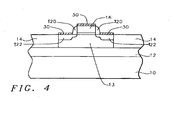
- Fig. 4 schematically illustrates in cross-sectional representation an example of a completed integrated circuit device fabricated by the process of the present invention.
- The present invention embodies one method for forming uniform ultrathin silicide features in the fabrication of an integrated circuit. The silicide features comprise titanium silicide, cobalt silicide, platinum silicide, tantalum silicide, nickel silicide, or palladium silicide and may have a spatial width of 100 nanometers (0.1 microns) or smaller. Alloy silicides of titanium, cobalt, platinum, tantalum, nickel, or palladium may also be used.
- The embodiment of the present invention will now be described with reference to Figs. 1 through 3. Referring to Fig. 1, there is shown an illustration of a portion of a partially completed integrated circuit. The
semiconductor substrate 10 is preferably composed of silicon having a (100) crystallographic orientation. The substrate may be an n- or p-type silicon. - An ultrathin film of cobalt acetate (Co(OAc)2) 20 is deposited over the surface of the substrate by a spin-on method to a thickness of between about 0.05 and 0.2 microns (500 and 2000 Angstroms).
- The cobalt acetate is subjected to a thermal treatment using the
metallic tips 15 to transform it to cobalt atlocations 22, as shown in Fig. 2 and 3. - Referring now to Fig. 2, an array of refractory
metallic tips 15 made of platinum, tantalum, titanium, or a metal nitride is heated to a temperature of between about 500 and 1200 °C and placed in contact with thethin film 20 at specific locations where the silicide features are to be formed for between about 10 and 20 seconds. The heated metallic tips contacting the thin film causes localized formation ofsilicide 22. Lines and features may be formed by maneuvering of the metallic tips. The metallic tips are aligned and patterned according to the desired layout. - Each of the metallic tips may be connected to a resistance heating source to ramp them up to the desired temperature. The material used for the tips typically have melting points much higher than the temperature required; that is, nearly twice. The metallic tips typically have a radius of curvature of about 100 nanometers. Such tips are usually used at the atomic level to estimate surface morphology using a technique called atomic force microscopy (AFM) or scanning tunneling microscopy (STM).
- The thermal treatment also comprises an atmosphere of H2 or N2 in a high vacuum or ultrahigh vacuum and a temperature of about 300 to 500 °C to less than about 900 °C. For example, high vacuum is between about 1.33 x 10⁻³ and 1.33 x 10⁻⁵ Pa (10-5 and 10-7 Torr) and ultrahigh vacuum is between about 1.33 x 10⁻⁸ and 1.33 x 10⁻⁹ Pa (10-10 and 10-11 Torr). The thermal treatment forms cobalt silicide lines or features 22 on the silicon substrate without oxidation of the metal surfaces. The unreacted
cobalt acetate film 20 is removed, for example using an organic solvent; e.g. ethanol, methanol, or isopropyl alcohol (IPA), leaving the metallic silicide features 22 on the silicon substrate , shown in figure 3 . - Alternatively, in the embodiment of the invention, nickel acetate, platinum acetate, or palladium acetate may be used in place of the cobalt acetate.
- This formation of silicide features can be incorporated into a typical transistor process flow. For example, as shown in Fig. 4, a typical transistor fabrication process flow includes formation of
shallow trench isolation 14,gate 16,sidewall spacers 120, and source/drain junctions 122. Subsequently, a thin layer of metal acetate is spin-coated. The metal acetate is transformed to metal silicide at specific areas according to the embodiment of the invention.Silicide 30 is formed, for example, on thegate 16 and over the source/drain regions 122. - The process of the invention is especially suited for fabricating ultrathin silicide films on silicon-on-insulator (SOI) substrates, as shown in Fig. 4 where
silicon 13 has been formed overlying the insulatinglayer 12. The main advantage for SOI applications is that no substrate heating is required which reduces any additional thermal stress induced on thesilicon channel 13 overlying thesilicon dioxide layer 12.
Claims (9)
- A method of fabricating silicide features in the manufacture of an integrated circuit device comprising:spin-coating a metal acetate layer (20) over the surface of a silicon semiconductor substrate (10);contacting said metal acetate layer (20) with an array of heated metallic tips (15) wherein said metallic tips are heated to a temperature of between 500 and 1200°C whereby said metal acetate layer is transformed to a metal silicide (22,30) where said metallic tips contact said metal acetate layer and wherein said metal acetate layer not contacted by said metallic tips is unreacted; andthereafter removing said unreacted metal acetate layer (20) leaving said metal silicide as said silicide features in the manufacture of said integrated circuit device.
- The method according to Claim 1 wherein said metal acetate layer comprises cobalt acetate and has a thickness of between 0.05 and 0.2 microns (500 and 2000 Angstroms).
- The method according to Claim 1 wherein said metallic tips comprise one of the group containing platinum, tantalum, and titanium.
- The method according to Claim 1 wherein said metallic tips comprise a refractory metal or a metal nitride.
- The method according to Claim 1 further comprising subjecting said integrated circuit device to a H2 or N2 atmosphere at high vacuum of between 1.33 x 10⁻³ and 1.33 x 10⁻⁵ Pa (10-5 and 10-7 Torr) to a temperature of between 300 and 500 °C to less than about 900 °C.
- The method according to Claim 1 further comprising subjecting said integrated circuit device to a H2 or N2 atmosphere at an ultrahigh vacuum of between 1.33 x 10⁻⁸ and 1.33 x 10⁻⁹ Pa (10-10 and 10-11 Torr) to a temperature of between 300 and 500 °C to less than about 900°C.
- The method according to claim 1 wherein said metal acetate layer (20) is contacted with said array of heated metallic tips (15) under vacuum whereby said metal acetate is not oxidized.
- The method according to Claim 1 wherein said metal acetate layer comprises one of the group containing, platinum acetate, nickel acetate, tantalum acetate, and palladium acetate and has a thickness of between 0.05 and 0.2 microns (500 and 2000 Angstroms).
- The method according to Claim 1 wherein said silicide features have a spatial width of less than 0.1 micron.
Applications Claiming Priority (2)
| Application Number | Priority Date | Filing Date | Title |
|---|---|---|---|
| US245994 | 1994-05-19 | ||
| US24599499A | 1999-02-05 | 1999-02-05 |
Publications (3)
| Publication Number | Publication Date |
|---|---|
| EP1026730A2 EP1026730A2 (en) | 2000-08-09 |
| EP1026730A3 EP1026730A3 (en) | 2004-01-21 |
| EP1026730B1 true EP1026730B1 (en) | 2006-12-13 |
Family
ID=22928925
Family Applications (1)
| Application Number | Title | Priority Date | Filing Date |
|---|---|---|---|
| EP00480019A Expired - Lifetime EP1026730B1 (en) | 1999-02-05 | 2000-02-03 | A method to form uniform silicide features |
Country Status (3)
| Country | Link |
|---|---|
| EP (1) | EP1026730B1 (en) |
| AT (1) | ATE348402T1 (en) |
| DE (1) | DE60032269T2 (en) |
Family Cites Families (1)
| Publication number | Priority date | Publication date | Assignee | Title |
|---|---|---|---|---|
| US5075243A (en) * | 1989-08-10 | 1991-12-24 | The United States Of America As Represented By The Administrator Of The National Aeronautics And Space Administration | Fabrication of nanometer single crystal metallic CoSi2 structures on Si |
-
2000
- 2000-02-03 AT AT00480019T patent/ATE348402T1/en not_active IP Right Cessation
- 2000-02-03 DE DE60032269T patent/DE60032269T2/en not_active Expired - Fee Related
- 2000-02-03 EP EP00480019A patent/EP1026730B1/en not_active Expired - Lifetime
Also Published As
| Publication number | Publication date |
|---|---|
| EP1026730A2 (en) | 2000-08-09 |
| EP1026730A3 (en) | 2004-01-21 |
| ATE348402T1 (en) | 2007-01-15 |
| DE60032269D1 (en) | 2007-01-25 |
| DE60032269T2 (en) | 2007-07-05 |
Similar Documents
| Publication | Publication Date | Title |
|---|---|---|
| US6153485A (en) | Salicide formation on narrow poly lines by pulling back of spacer | |
| US5780362A (en) | CoSi2 salicide method | |
| US5736461A (en) | Self-aligned cobalt silicide on MOS integrated circuits | |
| US6329276B1 (en) | Method of forming self-aligned silicide in semiconductor device | |
| US5937325A (en) | Formation of low resistivity titanium silicide gates in semiconductor integrated circuits | |
| US6562668B2 (en) | Method of fabricating thin film transistor using buffer layer and the thin film transistor | |
| JPH10229048A (en) | Method for manufacturing semiconductor device | |
| US5911114A (en) | Method of simultaneous formation of salicide and local interconnects in an integrated circuit structure | |
| US5162246A (en) | Selective germanium deposition on silicon and resulting structures | |
| US7625641B2 (en) | Method of forming a crystalline phase material | |
| JPH0758343A (en) | Method for manufacturing MIS transistor | |
| US6281117B1 (en) | Method to form uniform silicide features | |
| US6368949B1 (en) | Post-spacer etch surface treatment for improved silicide formation | |
| JP3175696B2 (en) | Method for manufacturing semiconductor device | |
| US6255181B1 (en) | Method for fabricating MOS semiconductor device having salicide region and LDD structure | |
| US7485572B2 (en) | Method for improved formation of cobalt silicide contacts in semiconductor devices | |
| US7029957B2 (en) | Method of manufacturing semiconductor device having thin film SOI structure | |
| EP1026730A2 (en) | A method to form uniform silicide features | |
| CN1300827C (en) | Stacked gate structure and method for manufacturing field effect transistor with the stacked gate structure | |
| TW447012B (en) | A method to form uniform silicide features | |
| EP0921560A2 (en) | Self-aligned contact | |
| JP3334692B2 (en) | Method for manufacturing semiconductor device | |
| US20020045344A1 (en) | Method of forming polycrystalline cosi2 salicide and products obtained thereof | |
| JPH05166752A (en) | Method for forming titanium silicide layer | |
| TWI222141B (en) | Semiconductor devices having a metal silicide bi-layer and the method for fabricating the same |
Legal Events
| Date | Code | Title | Description |
|---|---|---|---|
| PUAI | Public reference made under article 153(3) epc to a published international application that has entered the european phase |
Free format text: ORIGINAL CODE: 0009012 |
|
| AK | Designated contracting states |
Kind code of ref document: A2 Designated state(s): AT BE CH CY DE DK ES FI FR GB GR IE IT LI LU MC NL PT SE |
|
| AX | Request for extension of the european patent |
Free format text: AL;LT;LV;MK;RO;SI |
|
| PUAL | Search report despatched |
Free format text: ORIGINAL CODE: 0009013 |
|
| RIC1 | Information provided on ipc code assigned before grant |
Ipc: 7C 30B 1/02 B Ipc: 7C 23C 10/00 B Ipc: 7H 01L 21/285 A Ipc: 7C 23C 26/00 B |
|
| AK | Designated contracting states |
Kind code of ref document: A3 Designated state(s): AT BE CH CY DE DK ES FI FR GB GR IE IT LI LU MC NL PT SE |
|
| AX | Request for extension of the european patent |
Extension state: AL LT LV MK RO SI |
|
| 17P | Request for examination filed |
Effective date: 20040721 |
|
| AKX | Designation fees paid |
Designated state(s): AT BE CH CY DE DK ES FI FR GB GR IE IT LI LU MC NL PT SE |
|
| 17Q | First examination report despatched |
Effective date: 20040923 |
|
| GRAP | Despatch of communication of intention to grant a patent |
Free format text: ORIGINAL CODE: EPIDOSNIGR1 |
|
| GRAS | Grant fee paid |
Free format text: ORIGINAL CODE: EPIDOSNIGR3 |
|
| GRAA | (expected) grant |
Free format text: ORIGINAL CODE: 0009210 |
|
| AK | Designated contracting states |
Kind code of ref document: B1 Designated state(s): AT BE CH CY DE DK ES FI FR GB GR IE IT LI LU MC NL PT SE |
|
| PG25 | Lapsed in a contracting state [announced via postgrant information from national office to epo] |
Ref country code: IT Free format text: LAPSE BECAUSE OF FAILURE TO SUBMIT A TRANSLATION OF THE DESCRIPTION OR TO PAY THE FEE WITHIN THE PRE;WARNING: LAPSES OF ITALIAN PATENTS WITH EFFECTIVE DATE BEFORE 2007 MAY HAVE OCCURRED AT ANY TIME BEFORE 2007. THE CORRECT EFFECTIVE DATE MAY BE DIFFERENT FROM THE ONE RECORDED.SCRIBED TIME-LIMIT Effective date: 20061213 Ref country code: DK Free format text: LAPSE BECAUSE OF FAILURE TO SUBMIT A TRANSLATION OF THE DESCRIPTION OR TO PAY THE FEE WITHIN THE PRESCRIBED TIME-LIMIT Effective date: 20061213 Ref country code: LI Free format text: LAPSE BECAUSE OF FAILURE TO SUBMIT A TRANSLATION OF THE DESCRIPTION OR TO PAY THE FEE WITHIN THE PRESCRIBED TIME-LIMIT Effective date: 20061213 Ref country code: CH Free format text: LAPSE BECAUSE OF FAILURE TO SUBMIT A TRANSLATION OF THE DESCRIPTION OR TO PAY THE FEE WITHIN THE PRESCRIBED TIME-LIMIT Effective date: 20061213 Ref country code: NL Free format text: LAPSE BECAUSE OF FAILURE TO SUBMIT A TRANSLATION OF THE DESCRIPTION OR TO PAY THE FEE WITHIN THE PRESCRIBED TIME-LIMIT Effective date: 20061213 Ref country code: FI Free format text: LAPSE BECAUSE OF FAILURE TO SUBMIT A TRANSLATION OF THE DESCRIPTION OR TO PAY THE FEE WITHIN THE PRESCRIBED TIME-LIMIT Effective date: 20061213 Ref country code: AT Free format text: LAPSE BECAUSE OF FAILURE TO SUBMIT A TRANSLATION OF THE DESCRIPTION OR TO PAY THE FEE WITHIN THE PRESCRIBED TIME-LIMIT Effective date: 20061213 Ref country code: BE Free format text: LAPSE BECAUSE OF FAILURE TO SUBMIT A TRANSLATION OF THE DESCRIPTION OR TO PAY THE FEE WITHIN THE PRESCRIBED TIME-LIMIT Effective date: 20061213 |
|
| REG | Reference to a national code |
Ref country code: GB Ref legal event code: FG4D |
|
| REG | Reference to a national code |
Ref country code: CH Ref legal event code: EP |
|
| REG | Reference to a national code |
Ref country code: IE Ref legal event code: FG4D |
|
| REF | Corresponds to: |
Ref document number: 60032269 Country of ref document: DE Date of ref document: 20070125 Kind code of ref document: P |
|
| PG25 | Lapsed in a contracting state [announced via postgrant information from national office to epo] |
Ref country code: MC Free format text: LAPSE BECAUSE OF NON-PAYMENT OF DUE FEES Effective date: 20070228 |
|
| PG25 | Lapsed in a contracting state [announced via postgrant information from national office to epo] |
Ref country code: SE Free format text: LAPSE BECAUSE OF FAILURE TO SUBMIT A TRANSLATION OF THE DESCRIPTION OR TO PAY THE FEE WITHIN THE PRESCRIBED TIME-LIMIT Effective date: 20070313 |
|
| PG25 | Lapsed in a contracting state [announced via postgrant information from national office to epo] |
Ref country code: ES Free format text: LAPSE BECAUSE OF FAILURE TO SUBMIT A TRANSLATION OF THE DESCRIPTION OR TO PAY THE FEE WITHIN THE PRESCRIBED TIME-LIMIT Effective date: 20070324 |
|
| PG25 | Lapsed in a contracting state [announced via postgrant information from national office to epo] |
Ref country code: PT Free format text: LAPSE BECAUSE OF FAILURE TO SUBMIT A TRANSLATION OF THE DESCRIPTION OR TO PAY THE FEE WITHIN THE PRESCRIBED TIME-LIMIT Effective date: 20070514 |
|
| ET | Fr: translation filed | ||
| NLV1 | Nl: lapsed or annulled due to failure to fulfill the requirements of art. 29p and 29m of the patents act | ||
| REG | Reference to a national code |
Ref country code: CH Ref legal event code: PL |
|
| PLBE | No opposition filed within time limit |
Free format text: ORIGINAL CODE: 0009261 |
|
| STAA | Information on the status of an ep patent application or granted ep patent |
Free format text: STATUS: NO OPPOSITION FILED WITHIN TIME LIMIT |
|
| 26N | No opposition filed |
Effective date: 20070914 |
|
| GBPC | Gb: european patent ceased through non-payment of renewal fee |
Effective date: 20070313 |
|
| PG25 | Lapsed in a contracting state [announced via postgrant information from national office to epo] |
Ref country code: IE Free format text: LAPSE BECAUSE OF NON-PAYMENT OF DUE FEES Effective date: 20070205 |
|
| PG25 | Lapsed in a contracting state [announced via postgrant information from national office to epo] |
Ref country code: GB Free format text: LAPSE BECAUSE OF NON-PAYMENT OF DUE FEES Effective date: 20070313 Ref country code: GR Free format text: LAPSE BECAUSE OF FAILURE TO SUBMIT A TRANSLATION OF THE DESCRIPTION OR TO PAY THE FEE WITHIN THE PRESCRIBED TIME-LIMIT Effective date: 20070314 |
|
| PGFP | Annual fee paid to national office [announced via postgrant information from national office to epo] |
Ref country code: DE Payment date: 20080218 Year of fee payment: 9 |
|
| PGFP | Annual fee paid to national office [announced via postgrant information from national office to epo] |
Ref country code: FR Payment date: 20080229 Year of fee payment: 9 |
|
| PG25 | Lapsed in a contracting state [announced via postgrant information from national office to epo] |
Ref country code: CY Free format text: LAPSE BECAUSE OF FAILURE TO SUBMIT A TRANSLATION OF THE DESCRIPTION OR TO PAY THE FEE WITHIN THE PRESCRIBED TIME-LIMIT Effective date: 20061213 Ref country code: LU Free format text: LAPSE BECAUSE OF NON-PAYMENT OF DUE FEES Effective date: 20070203 |
|
| REG | Reference to a national code |
Ref country code: FR Ref legal event code: ST Effective date: 20091030 |
|
| PG25 | Lapsed in a contracting state [announced via postgrant information from national office to epo] |
Ref country code: DE Free format text: LAPSE BECAUSE OF NON-PAYMENT OF DUE FEES Effective date: 20090901 |
|
| PG25 | Lapsed in a contracting state [announced via postgrant information from national office to epo] |
Ref country code: FR Free format text: LAPSE BECAUSE OF NON-PAYMENT OF DUE FEES Effective date: 20090302 |