EP1024599A2 - Delay-locked-loop (DLL) having symmetrical rising and falling clock edge type delays - Google Patents
Delay-locked-loop (DLL) having symmetrical rising and falling clock edge type delays Download PDFInfo
- Publication number
- EP1024599A2 EP1024599A2 EP00101146A EP00101146A EP1024599A2 EP 1024599 A2 EP1024599 A2 EP 1024599A2 EP 00101146 A EP00101146 A EP 00101146A EP 00101146 A EP00101146 A EP 00101146A EP 1024599 A2 EP1024599 A2 EP 1024599A2
- Authority
- EP
- European Patent Office
- Prior art keywords
- pulses
- train
- input
- output
- pulse
- Prior art date
- Legal status (The legal status is an assumption and is not a legal conclusion. Google has not performed a legal analysis and makes no representation as to the accuracy of the status listed.)
- Granted
Links
Images

Classifications
-
- H—ELECTRICITY
- H03—ELECTRONIC CIRCUITRY
- H03L—AUTOMATIC CONTROL, STARTING, SYNCHRONISATION OR STABILISATION OF GENERATORS OF ELECTRONIC OSCILLATIONS OR PULSES
- H03L7/00—Automatic control of frequency or phase; Synchronisation
- H03L7/06—Automatic control of frequency or phase; Synchronisation using a reference signal applied to a frequency- or phase-locked loop
- H03L7/08—Details of the phase-locked loop
- H03L7/081—Details of the phase-locked loop provided with an additional controlled phase shifter
- H03L7/0812—Details of the phase-locked loop provided with an additional controlled phase shifter and where no voltage or current controlled oscillator is used
- H03L7/0814—Details of the phase-locked loop provided with an additional controlled phase shifter and where no voltage or current controlled oscillator is used the phase shifting device being digitally controlled
-
- G—PHYSICS
- G11—INFORMATION STORAGE
- G11C—STATIC STORES
- G11C7/00—Arrangements for writing information into, or reading information out from, a digital store
- G11C7/22—Read-write [R-W] timing or clocking circuits; Read-write [R-W] control signal generators or management
-
- B—PERFORMING OPERATIONS; TRANSPORTING
- B02—CRUSHING, PULVERISING, OR DISINTEGRATING; PREPARATORY TREATMENT OF GRAIN FOR MILLING
- B02C—CRUSHING, PULVERISING, OR DISINTEGRATING IN GENERAL; MILLING GRAIN
- B02C4/00—Crushing or disintegrating by roller mills
- B02C4/10—Crushing or disintegrating by roller mills with a roller co-operating with a stationary member
- B02C4/18—Crushing or disintegrating by roller mills with a roller co-operating with a stationary member in the form of a bar
- B02C4/20—Crushing or disintegrating by roller mills with a roller co-operating with a stationary member in the form of a bar wherein the roller is corrugated or toothed
-
- B—PERFORMING OPERATIONS; TRANSPORTING
- B02—CRUSHING, PULVERISING, OR DISINTEGRATING; PREPARATORY TREATMENT OF GRAIN FOR MILLING
- B02C—CRUSHING, PULVERISING, OR DISINTEGRATING IN GENERAL; MILLING GRAIN
- B02C4/00—Crushing or disintegrating by roller mills
- B02C4/28—Details
- B02C4/30—Shape or construction of rollers
-
- H—ELECTRICITY
- H03—ELECTRONIC CIRCUITRY
- H03L—AUTOMATIC CONTROL, STARTING, SYNCHRONISATION OR STABILISATION OF GENERATORS OF ELECTRONIC OSCILLATIONS OR PULSES
- H03L7/00—Automatic control of frequency or phase; Synchronisation
- H03L7/06—Automatic control of frequency or phase; Synchronisation using a reference signal applied to a frequency- or phase-locked loop
- H03L7/08—Details of the phase-locked loop
- H03L7/081—Details of the phase-locked loop provided with an additional controlled phase shifter
- H03L7/0812—Details of the phase-locked loop provided with an additional controlled phase shifter and where no voltage or current controlled oscillator is used
- H03L7/0816—Details of the phase-locked loop provided with an additional controlled phase shifter and where no voltage or current controlled oscillator is used the controlled phase shifter and the frequency- or phase-detection arrangement being connected to a common input
-
- H—ELECTRICITY
- H03—ELECTRONIC CIRCUITRY
- H03L—AUTOMATIC CONTROL, STARTING, SYNCHRONISATION OR STABILISATION OF GENERATORS OF ELECTRONIC OSCILLATIONS OR PULSES
- H03L7/00—Automatic control of frequency or phase; Synchronisation
- H03L7/06—Automatic control of frequency or phase; Synchronisation using a reference signal applied to a frequency- or phase-locked loop
- H03L7/08—Details of the phase-locked loop
- H03L7/085—Details of the phase-locked loop concerning mainly the frequency- or phase-detection arrangement including the filtering or amplification of its output signal
- H03L7/095—Details of the phase-locked loop concerning mainly the frequency- or phase-detection arrangement including the filtering or amplification of its output signal using a lock detector
Definitions
- This invention relates generally to delay-locked-loops.
- delay-locked-loops are used in a wide variety of applications in order to produce an output signal in-phase with a received signal, such as a train of input pulses.
- a received signal such as a train of input pulses.
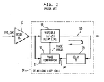
- FIG. 1 an input train of pulses, such as system clock pulses, SYS_CLK, are received by a receiver 12 (i.e., buffer) of an integrated circuit chip.
- the receiver 12 imparts a finite time delay, ⁇ , to the received pulses.
- a delay-locked-loop (DLL) 14 is sometimes provided.
- the delay-locked-loop 14 includes a phase comparator 16, a variable, typically digitally controlled, delay line 18, and a fixed delay 20.
- the fixed delay 20 has the same delay) ⁇ , as the receiver 12.
- the output of the receiver 12 i.e., input to the DLL 14
- the output of the DLL 14 is fed to one input 22 of the phase comparator 16 and the output of the DLL 14 is fed to another input 24 of the phase comparator 16.
- the output of the phase comparator 16 will force the time delay of the digitally controlled delay line 18 to a time delay nT- ⁇ , where T is the period of the clock pulses fed to the receiver 12 and n is an integer. That is, the output of the variable delay line 18 is feedback to input 24 of the phase comparator 16.
- the output of the phase comparator is a phase error signal.
- the phase error signal drives the delay of the delay line 18 such that the error is driven to zero.
- each pulse has a leading edge followed by a trailing edge.
- edges are of different edge types, i.e., the leading edge may be a rising edge type in which case the trailing edge will be a falling edge type; or, on the other hand, the leading edge may be a falling edge type in which case the trailing edge will be a rising edge type.
- DDR-SDRAMs Double-Data-Rate Synchronous Dynamic Random Access Memories
- NFETs n-channel field effect transistors
- PFETs p-channel field effect transistors
- the amount of current the PFET can source relative to the NFET varies thereby causing skew between propagation of rising and falling edge types in a PFET/NFET delay line (i.e., the rise delay of a clock pulse is different from the fall delay of the clock pulse).
- maximum operating objective data rate for example, a data rate of 200 MHz.
- ns nanoseconds
- processing variation effects can modulate rising and falling delays by approximately 0.5 ns.
- a circuit having: a receiver for receiving an input train of pulses and a delay-locked-loop coupled to an output of the receiver.
- the delay-locked-loop includes a pulse generator responsive to received input train of pulses produced at the output of the receiver for producing first pulses in response to the leading edges of the received input train of pulses and second pulses in response to the trailing edges of received input train of pulses.
- the leading edge of the first pulse has the same edge type as the leading edge of the second pulse (i.e., the leading edge of the first pulse and the leading edge of the second pulse are either both rising edge types or both falling edges types).
- the first pulses and the second pulses are combined into a composite input signal comprising the first and second pulses with the leading edge of the first pulse maintaining the same edge type.
- the delay-locked-loop also includes a variable delay line fed by the composite input signal for producing a composite output train of pulses comprising both the first train of pulses and the second train of pulses after a selected time delay provided by the delay line.
- the delay-locked-loop is responsive to one of the first train of pulses and the second train of pulses in the composite output train of pulses for selecting the time delay of the variable delay line so as to produce the composite output train of pulses with a predetermined phase relationship to the input train of pulses.
- both the leading edge and trailing edge of each of the received input pulses is represented by a pulse having the same leading edge type (i.e., the leading edge of the first pulse and the leading edge of the second pulse are both the same edge type; i.e., either both rising edge types or both falling edge types). Therefore, using the delay-locked-loop to operate in response to one of the first output pulses (i.e., pulses associated with the leading edge of the input train of pulses) or second output pulses (i.e., pulses associated with the trailing edge of the input train of pulses) assures proper phase alignment of both the leading and trailing edges of the input train of pulses.
- first output pulses i.e., pulses associated with the leading edge of the input train of pulses
- second output pulses i.e., pulses associated with the trailing edge of the input train of pulses
- the delay-locked-loop operates with the same edge type since such edge type is produced in response to both the leading and trailing edges of the received train of pulses.
- the delay characteristics of the delay line is the same for both leading and trailing edges of the input train of pulses, the output train of pulses is in proper time alignment with the input train of pulses.
- the delay-locked-loop includes a phase comparator for producing a control signal for the variable delay line in response to a time difference between pulses in the output train of pulses and pulses in the received train of input pulses.
- the delay-locked-loop includes a logic network for enabling only one of the first and second pulses to pass from the receiver to the delay line until the phase comparator provides an indication that the output train of pulses have rising edge types timed coincident with both the rising and falling edge types of the input train of pulses.
- the phase comparator includes a first input fed by pulses in the output train of pulses and a second input fed by pulses in the received train of input pulses.
- the delay-locked-loop includes: a gate fed by the output train of pulses and a gating signal; and a gate pulse generator responsive to one of the first and second pulses for producing the gating signal during the first pulse to enable the output train of pulses to pass through such gate to the phase comparator and to inhibit the output train of pulses from passing through the gate to the phase comparator during the second pulse.
- a method for generating a train of output pulses time having a predetermined time relationship with a train of input pulses.
- the method includes passing the input train of pulses through a receiver and producing a corresponding output train of pulses having leading and trailing edges timed coincident with both the leading and trailing edges of the input train of pulses.
- the producing step comprises: producing a first pulse in response to the leading edge of each one of the received input train of pulses and a second pulse in response to the trailing edge of each one of the received input train of clock pulses; and, feeding the first and second pulses through a delay line of a delay-locked-loop to produce at an output of the delay line the output train of pulses.
- the producing step includes producing a control signal for the variable delay line in response to a time difference between pulses in the output train of pulses and pulses in the received train of input pulses.
- the producing step comprises enabling only one of the first and second pulses to pass from the receiver to the delay line until an indication is provided that the output train of pulses have leading and trailing edges timed coincident with both the leading and trailing edges of the input train of pulses.
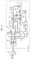
- a circuit 30 for receiving an input train of pulses, here system clock pulses, SYS_CLK (FIG. 3A).
- Each one of the pulses has a leading edge 31, here a rising edge type and a trailing edge 33, here a falling edge type, as shown in FIG. 3A.
- the circuit includes a delay-locked-loop (DLL) 32.
- the DLL 32 is responsive to both leading and trailing edges of the received input train of pulses and produces a corresponding output train of pulses DLL_OUT (FIG. 3F) having both leading and trailing edges with a predetermined phase alignment, here timed coincident, with both the leading and trailing edges of the input train of pulses SYS_CLK.
- the circuit 30 includes a receiver 33, typically a buffer amplifier, for receiving the input train of pulses SYS_CLK.
- the input train of pulses SYS_CLK has a period, T, as indicated in FIG. 3A.
- the receiver 33 provides a first time delay, ⁇ 1 to the pulses in the input train of pulses SYS_CLK, as indicated in FIG. 3B.
- the DLL 32 includes a pulse generating circuit 36, here a pair of one-shot multivibrators, for example, coupled to an output of the receiver 32.
- the one-shot multivibrators 36 produce a first pulse on line C0 (FIG. 3C), having a time duration less than T/2, in response to the leading edge of each one of the pulses in the input train of pulses and a second pulse on line C1 (FIG. 3D) in response to the trailing edge of each one of the pulses in the input train of pulses.
- Each one of the first pulses and each one of the second pulses have the same leading edge type; here, in this example, each one of the first pulses and each one of the second pulses have a rising edge type.
- the first and second pulses on lines C0 and C1 are shown in FIGS. 3C and 3D, respectively.
- the pulse generating circuit 36 produces the first pulses with a second time delay ⁇ 2 after the leading edge of the pulses produced at the output of receiver 33 and the second pulses with the second time delay ⁇ 2 after the leading edge of the pulses produced at the output of receiver 33.
- the logic network 50 includes a pair of AND gates 51, 53 fed by the pulses on lines C0 and C1, respectively, as shown.
- AND gate 51 is fed with a logic 1 signal.
- AND gate 53 is fed with a LOCK signal (FIG. 3H).
- the outputs of the AND gates 51, 53 are fed to inputs of an OR gate 55, as indicated.
- the logic network 50 enables only one of the first and second pulses, here only the first pulses on line C0, to pass from the pulse generator 36 to the delay line 34 during a start-up mode (i.e., until the phase comparator 42 provides an indication on line LOCK that the output train of pulses DLL_OUT have leading and trailing edges timed coincident with both the leading and trailing edges of the input train of pulses SYS_CLK fed to the receiver 33.
- the logic network 50 produces a composite output signal comprising the first pulses on line C0 and the second pulses on line C1, i.e., the signal DLL_IN as shown in FIG. 3E.
- the logic network 50 provides a delay ⁇ 3 to the first and second pulses fed thereto on lines C0 and C1, respectively.
- the gate 48 is used to gate "off' (i.e., inhibit) the pulses on line C1 until the DLL 32 is locked; i.e., when the "LOCK" signal goes to logic 1 as shown in FIG. 3H.
- the DLL 32 includes the variable, here digitally controlled, delay line 34.
- the variable delay line 34 is responsive to the first and second pulses and produces corresponding first and second output pulses on output 36.
- Each one of such first output pulse on line 36 which is a pulse having a rising leading edge produced in response to the rising edge of each pulse produced at the output of receiver 33, is produced in response to the corresponding one of the first pulses after a time delay ⁇ L selected in accordance with a control signal fed to the variable delay line 36 on line 38, in a manner to be described.
- the signal on line 38 is a phase error.
- each one of such second output pulse on line 36 which is a pulse having a rising leading edge produced in response to the trailing edge of each pulse produced at the output of receiver 33, is produced in response to the corresponding one of the second pulses after the same time delay ⁇ L selected in accordance with a control signal fed to the variable delay line 36 on line 38, in a manner to be described. That is, because the leading edges of both the first pulse on line C0 and second pulse on line C1 have the same edge types, here rising edge type, the delay line will produce the same delay ⁇ L to both the first pulse and the second pulse.
- the output of the variable delay line 34 produces the train of output pulses DLL_OUT on line 36, as indicated.
- the DLL 34 includes a delay network 40 fed by the output train of pulses DLL_OUT on line 36.
- the delay network 40 provides a time delay ⁇ 4 here equal to ⁇ 1 + ⁇ 2 (FIG. 3G).
- a phase comparator 42 having a first input 44 fed by one of the first and second pulses, here the first pulses on line C0 and a second input 46 coupled to an output of the delay network 46 through an AND gate 48, for producing the control signal on line 38.
- the control signal on line 38 selects the time delay ⁇ 3 equal to nT, where n is an integer, for the variable delay line 34 to produce the output pulses DLL_OUT on line 36 having leading edges and trailing edges timed coincident with the leading edges and trailing edges, respectively, of the pulses in the input train of pulses SYS_CLK fed to the receiver 33.
- n is an integer
- the logic network 50 enables only one of the first and second pulses, here only the first pulses on line C0, to pass from the receiver 33 to the delay line 34 until the phase comparator 42 provides an indication on line LOCK that the output train of pulses DLL_OUT delayed ⁇ 1 + ⁇ 2 fed thereto have leading and trailing edges timed coincident with the leading and trailing edges of the input train of pulses SYS_CLK fed to the receiver 33.
- the DLL gate 48 is fed by a time delayed version of the output train of pulses on line 36 and a time delayed gating signal produced by a gate pulse generator 52.
- the gate pulse generator 52 is a latch having an inverted set S input coupled to line C1 and an inverted reset input R coupled to line C0.
- the output of the gate pulse generator 52, Q is fed through a fixed delay line 57 (here providing a delay ⁇ 4 to Q to provide a delayed pulse Q D ) to an input of AND gate 48.
- the gate generator 52 is responsive to one of the first and second pulses and produces the gating signal on line Q.
- the signal on line Q is delayed by delay 57 to produce a delayed gating signal Q D , shown in FIG. 31, which is used during the first pulse to enable the output train of pulses to pass through such AND gate 48 to the phase comparator 42 and to inhibit the output train of pulses from passing through the AND gate 48 to the phase comparator 42 during the second pulse.
- a SET-RESET latch i.e., gate generator 52
- the gate generator 52 is RESET with the falling edge of the pulses on line C0 and SET with the falling edge of the pulses on line C1.
- the one shot pulse generator 36 produces pulses having rising leading edges
- such generator 36 may produce pulses having falling leading edges.
- a trailing edge time coincidence may be used and is an equivalent so long as both the first pulses and the second pulses have the same type edges (i.e., either a rising edge or a falling edge). That is, a first pulse produced in response to the trailing edge of the receiver output with the second pulse produced in response to the leading edge of the receiver output is equivalent to the circuit in FIG. 2 as long as both the first pulse and the second pulse have the same edge type (i.e., both rising or both falling).
- time coincidence i.e., a zero phase difference being the leading edges of the SYS_CLK and the leading edges of the output pulses DLL_OUT
- a fixed, non-zero phase difference may be used.
Landscapes
- Engineering & Computer Science (AREA)
- Food Science & Technology (AREA)
- Pulse Circuits (AREA)
- Stabilization Of Oscillater, Synchronisation, Frequency Synthesizers (AREA)
- Dram (AREA)
- Manipulation Of Pulses (AREA)
Abstract
Description
Claims (14)
- A circuit, comprising:a receiver for receiving an input train of pulses; anda delay-locked-loop coupled to an output of the receiver, the delay-locked-loop comprising:wherein the delay-locked-loop is responsive to one of the first train of pulses;and the second train of pulses in the composite output train of pulses for selecting the time delay of the variable delay line to produce such composite output train of pulses with a predetermined phase relationship with the input train of pulses.a pulse generator responsive to received input train of pulses produced at the output of the receiver for producing first pulses in response to the leading edges of the received input train of pulses and second pulses in response to the trailing edges of received input train of pulses, the leading edge of the first pulse having the same edge type as the leading edge of the second pulse;a logic network for combining the first pulses and the second pulses into a composite input signal comprising the first and second pulses with the leading edge of the first pulse maintaining the same edge type;a variable delay line fed by the composite input signal for producing a composite output train of pulses comprising both the first train of pulses and the second train of pulses after a selected time delay provided by the delay line; and
- The circuit recited in claim 1 wherein the delay-locked-loop includes a phase comparator for producing a control signal for the variable delay line in response to a time difference between pulses in the output train of pulses and pulses in the received train of input pulses.
- The circuit recited in claim 2 wherein the delay-locked-loop includes a logic network for enabling only one of the first and second pulses to pass from the receiver to the delay line until the phase comparator provides an indication that the output train of pulses have rising edge types timed coincident with both the rising and falling edge types of the input train of pulses.
- The circuit recited in claim 3 wherein the phase comparator includes a first input fed by pulses in the output train of pulses and a second input fed by pulses in the received train of input pulses and
wherein the delay-locked-loop includes:a gate fed by the output train of pulses and a gating signal; anda gate pulse generator responsive to one of the first and second pulses for producing the gating signal during the first pulse to enable the output train of pulses to pass through such gate to the phase comparator and to inhibit the output train of pulses from passing through the gate to the phase comparator during the second pulse. - The circuit recited in claim 2 wherein the phase comparator includes a first input fed by pulses in the output train of pulses and a second input fed by pulses in the received train of input pulses and
wherein the delay-locked-loop includes:a gate fed by the output train of pulses and a gating signal; anda gate pulse generator responsive to one of the first and second pulses for producing the gating signal during the first pulse to enable the output train of pulses to pass through such gate to the phase comparator and to inhibit the output train of pulses from passing through the gate to the phase comparator during the second pulse. - A circuit, comprising:a receiver for receiving an input train of pulses;a pulse generating circuit coupled to an output of the receiver for producing a first pulse in response to a leading edge of each one of the pulses in the input train of pulses and a second pulse in response to the trailing edge of each one of the pulses in the input train of pulses, the leading edges of the first and second pulses having the same edge type;a variable delay line responsive to the first and second pulses for producing corresponding first and second output pulses, each one of such first and second output pulses being produced in response to the corresponding one of the first and second pulses after a time delay selected in accordance with a control signal fed to the variable delay line;a phase comparator having a first input fed by one of the first and second pulses and a second input fed by the corresponding one of the first and second output pulses, for producing the control signal, such control signal selecting the time delay for the variable delay line to produce the output pulses with leading edges timed coincident with leading edges of the pulses in the input train of pulses.
- The circuit recited in claim 6 including:a logic network for enabling only one of the first and second pulses to pass from the receiver to the delay line until the phase comparator provides an indication that the output train of pulses have leading edges timed coincident with leading edges of the input train of pulses.
- The circuit recited in claim 7 wherein the phase comparator includes a first input fed by pulses in the output train of pulses and a second input fed by pulses in the received train of input pulses and including:a gate fed by the output train of pulses and a gating signal; anda gate pulse generator responsive to one of the first and second pulses for producing the gating signal during the first pulse to enable the output train of pulses to pass through such gate to the phase comparator and to inhibit the output train of pulses from passing through the gate to the phase comparator during the second pulse.
- The circuit recited in claim 6 wherein the phase comparator includes a first input fed by pulses in the output train of pulses and a second input fed by pulses in the received train of input pulses and including:a gate fed by the output train of pulses and a gating signal; anda gate pulse generator responsive to one of the first and second pulses for producing the gating signal during the first pulse to enable the output train of pulses to pass through such gate to the phase comparator and to inhibit the output train of pulses from passing through the gate to the phase comparator during the second pulse.
- A circuit, comprising:a receiver for receiving an input train of pulses such train of pulses having a period, T, such receiver providing a first time delay, Δ1 to the pulses in the input train of pulses;a pulse generating circuit coupled to an output of the receiver for producing a first pulse in response to a leading edge of each one of the pulses in the input train of pulses and a second pulse in response to a trailing edge of each one of the pulses in the input train of pulses, the leading edges of the first and second pulses having the same edge type, such pulse generating circuit producing the first pulses and the second pulses with a second time delay Δ2 after the leading edge of pulses in the input train of pulses;a logic network for combining the first pulses and the second pulses into a composite input signal comprising the first and second pulses with the leading edge of the first pulse maintaining the same edge type, such logic network providing a third time delay Δ3 to the first and second pulses;a variable delay line responsive to the first and second pulses for producing corresponding first and second output pulses, each one of such first and second output pulses being produced in response to the corresponding one of the first and second pulses after a time delay ΔL selected in accordance with a control signal fed to the variable delay line;a delay network fed by the output train of pulses such delay network providing a fourth time delay Δ4 related to Δ1+Δ2;a phase comparator having a first input fed by one of the first and second pulses and a second input coupled to an output of the delay network, for producing the control signal, such control signal selecting the time delay
- The circuit recited in claim 10 wherein the phase comparator includes a first input fed by pulses in the output train of pulses and a second input fed by pulses in the received train of input pulses and including:a gate fed by the output train of pulses and a gating signal; anda gate pulse generator responsive to one of the first and second pulses for producing the gating signal during the first pulse to enable the output train of pulses to pass through such gate to the phase comparator and to inhibit the output train of pulses from passing through the gate to the phase comparator during the second pulse.
- A method for generating a train of output pulses having a predetermined phase relationship with a train of input pulses, comprising:passing the input train of pulses through a receiver;producing a first pulse in response to the leading edge of each the received input train of pulses and a second pulse in response to the trailing edge of each one of the received input train of pulses, each one of the first and second pulses having leading edges with the same edge type;feeding the first and second pulses through a delay line to produce the output train of pulses.
- The method recited in claim 12 wherein the producing step includes producing a control signal for the variable delay line in response to a time difference between pulses in the output train of pulses and pulses in the received train of input pulses.
- The method recited in claim 13 wherein the producing step comprises enabling only one of the first and second pulses to pass from the receiver to the delay line until an indication is provided that the output train of pulses have leading edges timed coincident with the leading edges of the input train of pulses.
Applications Claiming Priority (2)
| Application Number | Priority Date | Filing Date | Title |
|---|---|---|---|
| US239487 | 1999-01-28 | ||
| US09/239,487 US6127866A (en) | 1999-01-28 | 1999-01-28 | Delay-locked-loop (DLL) having symmetrical rising and falling clock edge type delays |
Publications (3)
| Publication Number | Publication Date |
|---|---|
| EP1024599A2 true EP1024599A2 (en) | 2000-08-02 |
| EP1024599A3 EP1024599A3 (en) | 2004-06-16 |
| EP1024599B1 EP1024599B1 (en) | 2006-04-05 |
Family
ID=22902368
Family Applications (1)
| Application Number | Title | Priority Date | Filing Date |
|---|---|---|---|
| EP00101146A Expired - Lifetime EP1024599B1 (en) | 1999-01-28 | 2000-01-21 | Delay-locked-loop (DLL) having symmetrical rising and falling clock edge type delays |
Country Status (7)
| Country | Link |
|---|---|
| US (1) | US6127866A (en) |
| EP (1) | EP1024599B1 (en) |
| JP (1) | JP2000236242A (en) |
| KR (1) | KR100614721B1 (en) |
| CN (1) | CN1166062C (en) |
| DE (1) | DE60027065T2 (en) |
| TW (1) | TW477117B (en) |
Cited By (1)
| Publication number | Priority date | Publication date | Assignee | Title |
|---|---|---|---|---|
| EP1139569A1 (en) * | 2000-03-31 | 2001-10-04 | Samsung Electronics Co., Ltd. | Adjustment of the duty-cycle of a periodic digital signal with leading and triling edge DLLs |
Families Citing this family (19)
| Publication number | Priority date | Publication date | Assignee | Title |
|---|---|---|---|---|
| US6765976B1 (en) | 2000-03-29 | 2004-07-20 | G-Link Technology | Delay-locked loop for differential clock signals |
| US6411142B1 (en) * | 2000-12-06 | 2002-06-25 | Ati International, Srl | Common bias and differential structure based DLL with fast lockup circuit and current range calibration for process variation |
| US6346838B1 (en) * | 2001-01-05 | 2002-02-12 | Taiwan Semiconductor Manufacturing Corporation | Internal offset-canceled phase locked loop-based deskew buffer |
| US6456130B1 (en) | 2001-01-11 | 2002-09-24 | Infineon Technologies Ag | Delay lock loop and update method with limited drift and improved power savings |
| US6492852B2 (en) | 2001-03-30 | 2002-12-10 | International Business Machines Corporation | Pre-divider architecture for low power in a digital delay locked loop |
| JP3556649B2 (en) * | 2002-07-26 | 2004-08-18 | 沖電気工業株式会社 | Memory abnormal operation detection circuit, integrated circuit, and abnormal operation detection method |
| US6903586B2 (en) * | 2003-02-28 | 2005-06-07 | Ati Technologies, Inc. | Gain control circuitry for delay locked loop circuit |
| US6822484B1 (en) * | 2003-06-26 | 2004-11-23 | International Business Machines Corporation | High-frequency phase/frequency detector with improved reset mechanism |
| US20050086424A1 (en) * | 2003-10-21 | 2005-04-21 | Infineon Technologies North America Corp. | Well-matched echo clock in memory system |
| DE10354818B3 (en) * | 2003-11-24 | 2005-02-17 | Infineon Technologies Ag | Clock signal input/output device for clock signal correction e.g. for semiconductor memory device, has frequency divider, signal integrator and two signal receiver circuits coupled to signal restoration circuit |
| CN1735081B (en) * | 2004-08-11 | 2010-10-06 | 华为技术有限公司 | Control method and circuit for output signal waveform of line driver |
| KR100652394B1 (en) | 2005-01-07 | 2006-12-01 | 삼성전자주식회사 | Rising / polling time control device of transmitter's output signal |
| DE102005036559B3 (en) * | 2005-08-03 | 2007-01-04 | Infineon Technologies Ag | Apparatus and method for synchronizing clock signals and controlling the duty cycles of the clock signal |
| GB2429590A (en) * | 2005-08-23 | 2007-02-28 | Zarlink Semiconductor Ltd | Variable delay circuit |
| US8031005B2 (en) * | 2009-03-23 | 2011-10-04 | Qualcomm, Incorporated | Amplifier supporting multiple gain modes |
| CN104485954B (en) * | 2014-10-31 | 2018-01-05 | 江汉大学 | The control method and time device of a kind of time device |
| US10944385B1 (en) * | 2020-01-17 | 2021-03-09 | Qualcomm Incorporated | Delay circuit that accurately maintains input duty cycle |
| TWI732558B (en) * | 2020-05-18 | 2021-07-01 | 華邦電子股份有限公司 | Delay-locked loop device and operation method thereof |
| KR20250122686A (en) * | 2024-02-07 | 2025-08-14 | 다믈파워반도체 유한회사 | Apparatus for Providing Delay Locked Loop for Duty Cycle Correction |
Family Cites Families (5)
| Publication number | Priority date | Publication date | Assignee | Title |
|---|---|---|---|---|
| US3982195A (en) * | 1975-05-29 | 1976-09-21 | Teletype Corporation | Method and apparatus for decoding diphase signals |
| US4984255A (en) * | 1989-11-15 | 1991-01-08 | National Semiconductor Corporation | Edge transition insensitive delay line system and method |
| DE4231175C1 (en) * | 1992-09-17 | 1994-01-13 | Siemens Ag | Arrangement for clock recovery |
| US5675273A (en) * | 1995-09-08 | 1997-10-07 | International Business Machines Corporation | Clock regulator with precision midcycle edge timing |
| JP3688392B2 (en) * | 1996-05-31 | 2005-08-24 | 三菱電機株式会社 | Waveform shaping device and clock supply device |
-
1999
- 1999-01-28 US US09/239,487 patent/US6127866A/en not_active Expired - Lifetime
-
2000
- 2000-01-21 EP EP00101146A patent/EP1024599B1/en not_active Expired - Lifetime
- 2000-01-21 DE DE60027065T patent/DE60027065T2/en not_active Expired - Lifetime
- 2000-01-26 JP JP2000017125A patent/JP2000236242A/en active Pending
- 2000-01-28 CN CNB001019279A patent/CN1166062C/en not_active Expired - Lifetime
- 2000-01-28 KR KR1020000004226A patent/KR100614721B1/en not_active Expired - Fee Related
- 2000-02-09 TW TW089101396A patent/TW477117B/en not_active IP Right Cessation
Cited By (2)
| Publication number | Priority date | Publication date | Assignee | Title |
|---|---|---|---|---|
| EP1139569A1 (en) * | 2000-03-31 | 2001-10-04 | Samsung Electronics Co., Ltd. | Adjustment of the duty-cycle of a periodic digital signal with leading and triling edge DLLs |
| US6452432B2 (en) | 2000-03-31 | 2002-09-17 | Samsung Electronics Co., Ltd. | Signal processing circuits having a pair of delay locked loop (DLL) circuits for adjusting a duty-cycle of a periodic digital signal and methods of operating same |
Also Published As
| Publication number | Publication date |
|---|---|
| JP2000236242A (en) | 2000-08-29 |
| KR20000071314A (en) | 2000-11-25 |
| CN1166062C (en) | 2004-09-08 |
| EP1024599A3 (en) | 2004-06-16 |
| DE60027065D1 (en) | 2006-05-18 |
| KR100614721B1 (en) | 2006-08-21 |
| EP1024599B1 (en) | 2006-04-05 |
| TW477117B (en) | 2002-02-21 |
| US6127866A (en) | 2000-10-03 |
| DE60027065T2 (en) | 2006-10-05 |
| CN1263382A (en) | 2000-08-16 |
Similar Documents
| Publication | Publication Date | Title |
|---|---|---|
| US6127866A (en) | Delay-locked-loop (DLL) having symmetrical rising and falling clock edge type delays | |
| US6657918B2 (en) | Delayed locked loop implementation in a synchronous dynamic random access memory | |
| US7605626B2 (en) | Clock generator and clock duty cycle correction method | |
| US6750688B2 (en) | Semiconductor integrated circuit device and delay-locked loop device | |
| US7111184B2 (en) | System and method for deterministic communication across clock domains | |
| EP0964517A2 (en) | Delay locked loop | |
| US7814359B2 (en) | High-speed phase-adjusted quadrature data rate (QDR) transceiver and method thereof | |
| US6242960B1 (en) | Internal clock signal generating circuit employing pulse generator | |
| KR19980078283A (en) | Clock Phase Comparators | |
| KR20220046104A (en) | Duty correction device and method, a semiconductor appratus using the same | |
| US7840830B2 (en) | Semiconductor integrated circuit having data input apparatus and method of inputting data using the same | |
| US20050044441A1 (en) | Memory device for compensating for a clock skew causing a centering error and a method of compensating for the clock skew | |
| US20020053932A1 (en) | System and method for eliminating pulse width variations in digital delay lines | |
| US6066968A (en) | Delay lock loop circuit for semiconductor memory device | |
| JP2007151102A (en) | Line skew minimizer | |
| US5742194A (en) | Internal clock generator for a synchronous dynamic RAM | |
| KR100346835B1 (en) | Semiconductor memory device implementing high speed operation of delay locked loop | |
| US6633995B1 (en) | System for generating N pipeline control signals by delaying at least one control signal corresponding to a subsequent data path circuit | |
| US6255883B1 (en) | System and method for balancing clock distribution between two devices | |
| US5825834A (en) | Fast response system implementing a sampling clock for extracting stable clock information from a serial data stream with defined jitter characeristics and method therefor | |
| HK1030109A (en) | Delay-locked-loop (dll) having symmetrical rising and falling clock edge type delays | |
| KR102570959B1 (en) | Integrated circuit | |
| KR20000031806A (en) | Internal clock generation circuit in semiconductor device | |
| KR20190134037A (en) | Semiconductor apparatus with domain crossing |
Legal Events
| Date | Code | Title | Description |
|---|---|---|---|
| PUAI | Public reference made under article 153(3) epc to a published international application that has entered the european phase |
Free format text: ORIGINAL CODE: 0009012 |
|
| AK | Designated contracting states |
Kind code of ref document: A2 Designated state(s): AT BE CH CY DE DK ES FI FR GB GR IE IT LI LU MC NL PT SE |
|
| AX | Request for extension of the european patent |
Free format text: AL;LT;LV;MK;RO;SI |
|
| PUAL | Search report despatched |
Free format text: ORIGINAL CODE: 0009013 |
|
| RAP1 | Party data changed (applicant data changed or rights of an application transferred) |
Owner name: INTERNATIONAL BUSINESS MACHINES CORPORATION Owner name: INFINEON TECHNOLOGIES AG |
|
| AK | Designated contracting states |
Kind code of ref document: A3 Designated state(s): AT BE CH CY DE DK ES FI FR GB GR IE IT LI LU MC NL PT SE |
|
| AX | Request for extension of the european patent |
Extension state: AL LT LV MK RO SI |
|
| 17P | Request for examination filed |
Effective date: 20040630 |
|
| AKX | Designation fees paid |
Designated state(s): DE GB IE |
|
| 17Q | First examination report despatched |
Effective date: 20050310 |
|
| RBV | Designated contracting states (corrected) |
Designated state(s): DE GB IE |
|
| GRAP | Despatch of communication of intention to grant a patent |
Free format text: ORIGINAL CODE: EPIDOSNIGR1 |
|
| GRAS | Grant fee paid |
Free format text: ORIGINAL CODE: EPIDOSNIGR3 |
|
| GRAA | (expected) grant |
Free format text: ORIGINAL CODE: 0009210 |
|
| AK | Designated contracting states |
Kind code of ref document: B1 Designated state(s): DE GB IE |
|
| REG | Reference to a national code |
Ref country code: GB Ref legal event code: FG4D |
|
| REG | Reference to a national code |
Ref country code: IE Ref legal event code: FG4D |
|
| REF | Corresponds to: |
Ref document number: 60027065 Country of ref document: DE Date of ref document: 20060518 Kind code of ref document: P |
|
| PGFP | Annual fee paid to national office [announced via postgrant information from national office to epo] |
Ref country code: GB Payment date: 20070119 Year of fee payment: 8 |
|
| PLBE | No opposition filed within time limit |
Free format text: ORIGINAL CODE: 0009261 |
|
| STAA | Information on the status of an ep patent application or granted ep patent |
Free format text: STATUS: NO OPPOSITION FILED WITHIN TIME LIMIT |
|
| 26N | No opposition filed |
Effective date: 20070108 |
|
| GBPC | Gb: european patent ceased through non-payment of renewal fee |
Effective date: 20080121 |
|
| PG25 | Lapsed in a contracting state [announced via postgrant information from national office to epo] |
Ref country code: GB Free format text: LAPSE BECAUSE OF NON-PAYMENT OF DUE FEES Effective date: 20080121 |
|
| REG | Reference to a national code |
Ref country code: DE Ref legal event code: R081 Ref document number: 60027065 Country of ref document: DE Owner name: INTERNATIONAL BUSINESS MACHINES CORPORATION, A, US Free format text: FORMER OWNER: IBM INTERNATIONAL BUSINESS MACH, QIMONDA AG, , US Ref country code: DE Ref legal event code: R081 Ref document number: 60027065 Country of ref document: DE Owner name: INFINEON TECHNOLOGIES AG, DE Free format text: FORMER OWNER: IBM INTERNATIONAL BUSINESS MACH, QIMONDA AG, , US Ref country code: DE Ref legal event code: R081 Ref document number: 60027065 Country of ref document: DE Owner name: INTERNATIONAL BUSINESS MACHINES CORPORATION, A, US Free format text: FORMER OWNERS: IBM INTERNATIONAL BUSINESS MACHINES CORPORATION, ARMONK, N.Y., US; QIMONDA AG, 81739 MUENCHEN, DE Ref country code: DE Ref legal event code: R081 Ref document number: 60027065 Country of ref document: DE Owner name: INFINEON TECHNOLOGIES AG, DE Free format text: FORMER OWNERS: IBM INTERNATIONAL BUSINESS MACHINES CORPORATION, ARMONK, N.Y., US; QIMONDA AG, 81739 MUENCHEN, DE Ref country code: DE Ref legal event code: R081 Ref document number: 60027065 Country of ref document: DE Owner name: GLOBALFOUNDRIES US 2 LLC (N.D.GES.DES STAATES , US Free format text: FORMER OWNERS: IBM INTERNATIONAL BUSINESS MACHINES CORPORATION, ARMONK, N.Y., US; QIMONDA AG, 81739 MUENCHEN, DE Ref country code: DE Ref legal event code: R081 Ref document number: 60027065 Country of ref document: DE Owner name: GLOBALFOUNDRIES INC., KY Free format text: FORMER OWNERS: IBM INTERNATIONAL BUSINESS MACHINES CORPORATION, ARMONK, N.Y., US; QIMONDA AG, 81739 MUENCHEN, DE |
|
| PGFP | Annual fee paid to national office [announced via postgrant information from national office to epo] |
Ref country code: IE Payment date: 20160122 Year of fee payment: 17 |
|
| REG | Reference to a national code |
Ref country code: DE Ref legal event code: R081 Ref document number: 60027065 Country of ref document: DE Owner name: INFINEON TECHNOLOGIES AG, DE Free format text: FORMER OWNERS: INFINEON TECHNOLOGIES AG, 85579 NEUBIBERG, DE; INTERNATIONAL BUSINESS MACHINES CORPORATION, ARMONK, NY, US Ref country code: DE Ref legal event code: R081 Ref document number: 60027065 Country of ref document: DE Owner name: GLOBALFOUNDRIES INC., KY Free format text: FORMER OWNERS: INFINEON TECHNOLOGIES AG, 85579 NEUBIBERG, DE; INTERNATIONAL BUSINESS MACHINES CORPORATION, ARMONK, NY, US Ref country code: DE Ref legal event code: R081 Ref document number: 60027065 Country of ref document: DE Owner name: GLOBALFOUNDRIES INC., KY Free format text: FORMER OWNERS: INFINEON TECHNOLOGIES AG, 85579 NEUBIBERG, DE; INTERNATIONAL BUSINESS MACHINES CORPORATION, ARMONK, N.Y., US Ref country code: DE Ref legal event code: R081 Ref document number: 60027065 Country of ref document: DE Owner name: INFINEON TECHNOLOGIES AG, DE Free format text: FORMER OWNERS: INFINEON TECHNOLOGIES AG, 85579 NEUBIBERG, DE; INTERNATIONAL BUSINESS MACHINES CORPORATION, ARMONK, N.Y., US |
|
| REG | Reference to a national code |
Ref country code: DE Ref legal event code: R081 Ref document number: 60027065 Country of ref document: DE Owner name: GLOBALFOUNDRIES INC., KY Free format text: FORMER OWNERS: GLOBALFOUNDRIES US 2 LLC (N.D.GES.DES STAATES DELAWARE), HOPEWELL JUNCTION, N.Y., US; INFINEON TECHNOLOGIES AG, 85579 NEUBIBERG, DE Ref country code: DE Ref legal event code: R082 Ref document number: 60027065 Country of ref document: DE Representative=s name: RICHARDT PATENTANWAELTE PARTG MBB, DE Ref country code: DE Ref legal event code: R081 Ref document number: 60027065 Country of ref document: DE Owner name: INFINEON TECHNOLOGIES AG, DE Free format text: FORMER OWNERS: GLOBALFOUNDRIES US 2 LLC (N.D.GES.DES STAATES DELAWARE), HOPEWELL JUNCTION, N.Y., US; INFINEON TECHNOLOGIES AG, 85579 NEUBIBERG, DE |
|
| REG | Reference to a national code |
Ref country code: IE Ref legal event code: MM4A |
|
| PG25 | Lapsed in a contracting state [announced via postgrant information from national office to epo] |
Ref country code: IE Free format text: LAPSE BECAUSE OF NON-PAYMENT OF DUE FEES Effective date: 20170121 |
|
| PGFP | Annual fee paid to national office [announced via postgrant information from national office to epo] |
Ref country code: DE Payment date: 20190604 Year of fee payment: 20 |
|
| REG | Reference to a national code |
Ref country code: DE Ref legal event code: R071 Ref document number: 60027065 Country of ref document: DE |