EP1023623B1 - Cantilevered glass structures for nanodelivery of chemicals - Google Patents
Cantilevered glass structures for nanodelivery of chemicals Download PDFInfo
- Publication number
- EP1023623B1 EP1023623B1 EP98903774A EP98903774A EP1023623B1 EP 1023623 B1 EP1023623 B1 EP 1023623B1 EP 98903774 A EP98903774 A EP 98903774A EP 98903774 A EP98903774 A EP 98903774A EP 1023623 B1 EP1023623 B1 EP 1023623B1
- Authority
- EP
- European Patent Office
- Prior art keywords
- micropipette
- tip
- tapered
- chemicals
- glass
- Prior art date
- Legal status (The legal status is an assumption and is not a legal conclusion. Google has not performed a legal analysis and makes no representation as to the accuracy of the status listed.)
- Expired - Lifetime
Links
Images


Classifications
-
- G—PHYSICS
- G02—OPTICS
- G02B—OPTICAL ELEMENTS, SYSTEMS OR APPARATUS
- G02B6/00—Light guides; Structural details of arrangements comprising light guides and other optical elements, e.g. couplings
- G02B6/24—Coupling light guides
- G02B6/255—Splicing of light guides, e.g. by fusion or bonding
- G02B6/2552—Splicing of light guides, e.g. by fusion or bonding reshaping or reforming of light guides for coupling using thermal heating, e.g. tapering, forming of a lens on light guide ends
-
- G—PHYSICS
- G01—MEASURING; TESTING
- G01Q—SCANNING-PROBE TECHNIQUES OR APPARATUS; APPLICATIONS OF SCANNING-PROBE TECHNIQUES, e.g. SCANNING PROBE MICROSCOPY [SPM]
- G01Q60/00—Particular types of SPM [Scanning Probe Microscopy] or microscopes; Essential components thereof
- G01Q60/18—SNOM [Scanning Near-Field Optical Microscopy] or apparatus therefor, e.g. SNOM probes
- G01Q60/22—Probes, their manufacture, or their related instrumentation, e.g. holders
-
- G—PHYSICS
- G02—OPTICS
- G02B—OPTICAL ELEMENTS, SYSTEMS OR APPARATUS
- G02B6/00—Light guides; Structural details of arrangements comprising light guides and other optical elements, e.g. couplings
- G02B6/24—Coupling light guides
- G02B6/241—Light guide terminations
Definitions
- This invention is based on advances in near-field optics.
- the objective is to develop optical elements that can illuminate, detect and/or enhance optical phenomena within a distance, from the object, that is considerably less than the dimensions of one wavelength.
- Conventional optical instruments all of which work in the far-field are based on lenses which critically depend on the wave nature of light. Thus, these elements are inherently limited to operation in the far-field with associated problems of diffraction that intrinsically limits resolution to approximately half the wavelength of light.
- Near-field optical elements not only overcome this diffraction limit of resolution but also relax the wavelength dependence of optical resolution. In its simplest implementation [ A. Lewis, M. Isaacson, A. Hartoonian and A. Murray, Biophysical J.
- near-field optics involves transmitting light through a subwavelength aperture that is brought in close proximity to a surface. The sample or the aperture is then scanned in order to obtain an image or create a pattern with the subwavelength spot of light that emanates from this near-field optical element.
- the initial taper dimension is chosen to be approximately 20 microns in diameter for region of 100 microns length just above the second taper (see Figure 4 a) . This is the region in straight fibers that the flexibility of the structure is monitored. This dimensionality controls the resonance frequency and this frequency, f, can be altered up to 500 kHz with a width of the resonance, ⁇ f, that can be 0.75 kHz.
- Fibers are bent at the tip according to the procedure that is described by K. Lieberman and A. Lewis, "A Method and a Device for Probe Microscopy" [PCT Application Serial Number PCT/US94/08691 ].
- This bent fiber structure is seen in Figure 5 .
- the angle of the bend in this structure is between 45-60°.
- the pulling, coating and the resulting resonance frequencies are the same except that the angle of the coating is 85°.
- such elements can be used for the dynamic sensing of surface movement initiated by an external stimulus such as light, sound, electricity etc.
- a liquid or a gas is transmitted through the narrow opening at the tip of the cantilevered micropipette.
- Such an uncoated tapered micropipette with force sensing capabilities and a reflective coating only on the cantilever allows the tip to be brought into contact with a surface and this permits the delivery of nanoquantities of material onto the surface. This causes a chemical change on appropriately chosen surfaces if the nature of the chemical in the tip and the chemical in the surface are reactive one with the other.
- the tip is accomplished by pressure of the liquid column, by chemical manipulation of the hydrophillicity of the surface and the tip and by the nature of the tip geometry. Specifically on this last parameter the requirement is exactly opposite to what is required for the light funnels tips discussed above.
- the cone angle of the tip can be as small as 7°. This prevents spreading of the liquid column. Measured resonance frequencies of these structures have been measured at 200 kHz.
- the pulling and coating parameters are similar to those that are described in the tips that are used for chemical delivery.
- optimization of the force sensing capabilities of the probes described above is achieved by modulating the dimension of the taper of the glass in the region where the flexibility of the structure is monitored and this results in a resonance that is controlled in frequency.
- the frequency, f can be altered by up to 500 kHz with a width of the resonance, ⁇ f, that can be 0.75 kHz. This allows for maximal response of the tips to dynamic movements of the surface and/or the maximal sensitivity of the tips for the application of non-contact protocols in measuring surface forces.
- FIG. 8 To achieve appropriate coatings a device was constructed as shown in Figure 8 .
- This device is based on vacuum bell jar and consists of a base 8.1, rotating sealed shaft 8.2, electromotor 8.3, drive gear wheel 8.4 and set of driven gear wheels 8.5 that are mounted on the periphery of a cup 8.6.
- Rotating mounts 8.7 of tapered straight and/or cantilevered micropipettes and fibers 8.8 are mounted on pillars 8.9 and connected with driven wheel axles by flexible shafts 8.10.
- the device operates as following:
- the motor 8.3 rotates shaft 8.2, which rotates wheel 8.4 and wheels 8.5.
- the rotary motion is transmitted on mounts 8.7 with fibers 8.8 by shafts 8.10.
- the angle of the tapered glass elements may be changed by a mount that can be raised and lowered and can turn around on the axle 8.11. So that the rotation of the tapered straight or cantilevered micropipette or fiber during the coating process provides uniformity of deposition, and its rotation provides the opportunity to prevent the coating of the tip itself.
Landscapes
- Physics & Mathematics (AREA)
- General Physics & Mathematics (AREA)
- Engineering & Computer Science (AREA)
- General Health & Medical Sciences (AREA)
- Nuclear Medicine, Radiotherapy & Molecular Imaging (AREA)
- Radiology & Medical Imaging (AREA)
- Health & Medical Sciences (AREA)
- Plasma & Fusion (AREA)
- Optics & Photonics (AREA)
- Optical Fibers, Optical Fiber Cores, And Optical Fiber Bundles (AREA)
- Surface Treatment Of Glass (AREA)
- Length Measuring Devices Characterised By Use Of Acoustic Means (AREA)
- Physical Or Chemical Processes And Apparatus (AREA)
- Manufacture, Treatment Of Glass Fibers (AREA)
Abstract
Description
- This invention allows the use of tapered cantilevered structures that are optimized for the maximal nanodelivery of chemicals. These structures are generated so that they can simultaneously act as force sensors with excellent dynamic characteristics. Unlike previous attempts at obtaining such elements with chemical etching techniques our methodology is based solely on the application of glass pulling technologies with specific protocols that can minimize the subwavelength travel of light waves and can maximize the dynamic capabilities of these devices. Unlike the glass etching techniques these glass pulling technologies are universally applicable to glass micropipettes and fibers. Optimal geometries of force sensing glass micropipettes are invented for the optimal delivery of chemicals in nanoquantities in a defined and in a nanometrically controlled fashion.
- This invention is based on advances in near-field optics.
- Near-field optics is the development of optical elements that can work in the near-field of an object that is to be interrogated by light.
- In essence, the objective is to develop optical elements that can illuminate, detect and/or enhance optical phenomena within a distance, from the object, that is considerably less than the dimensions of one wavelength. Conventional optical instruments all of which work in the far-field are based on lenses which critically depend on the wave nature of light. Thus, these elements are inherently limited to operation in the far-field with associated problems of diffraction that intrinsically limits resolution to approximately half the wavelength of light. Near-field optical elements not only overcome this diffraction limit of resolution but also relax the wavelength dependence of optical resolution. In its simplest implementation [A. Lewis, M. Isaacson, A. Hartoonian and A. Murray, Biophysical J. 41, 405a (1983); Ultramicroscopy 13, 227 (1984)] near-field optics involves transmitting light through a subwavelength aperture that is brought in close proximity to a surface. The sample or the aperture is then scanned in order to obtain an image or create a pattern with the subwavelength spot of light that emanates from this near-field optical element.
- The method of choice that is used throughout the world today to produce near-field optical elements was developed by Lewis et al. [United States Patent Number
4,917,462 ]. The essence of the methodology of Lewis et al was to use heating, tension and pulling with microprocessor control to produce tapered glass structures that were subsequently coated with metal to form a subwavelength aperture. This was a simple, cheap and reliable method of producing these subwavelength optical elements. Nonetheless, these elements were produced without much regard to the geometry of the subwavelength tip in terms of reducing the subwavelength region through which the light wave traversed. It is important to realize that the technology in the Lewis et al patent was a general methodology for producing these subwavelength tips through which subwavelength points of light could be produced. This generality can be seen by the fact that the same technology could be used to produce tapered optical elements made out of glass capillaries [A. Harootunian, E. Betzig, M. S. Isaacson and A. Lewis, Appl. Phys. Lett. 49, 674 (1986)] or glass fibers [Betzig E., Trautman J. K., Harris T. D., Weiner J. S. and Kostelak R. L., Science 251, 1468 (1991)]. All of these structures, however, had less than optimized geometries at the tip and thus there were significant evanescent losses that resulted from the transmission of the electromagnetic radiation through the tip. - The first attempts at resolving this problem were made by workers who realized that geometries at the tip that were closer to what would be optimal for high transmission of the light wave through the subwavelength region could be approached with chemical etching of glass fibers [Ohtsu, M., S. Juang, T. Pangaribuan and M. Kozuma, Proceesing of NFO-1, 131-139 (1993); Jiang, S., Ohsawa, H., Yamada, K., Pangaribuan, T., Ohtsu, M., Imai, K., and Ikai, A., Jpn. J. Appl. Phys. 31, 2282 (1992)] without any previous tapering. Such structures had the potential to generate high throughputs if the coating of these structures could be effectively performed. The coating, however, was problematic since the etching technology resulted in damaged surfaces that were difficult to impossible to coat successfully. In addition, the angle required for coating such an etched structure was not compatible with the geometry of such untapered etched fibers. Furthermore, the geometry of such untapered elements (see
Figure 1 ) perturbed significantly the ability of such elements to track rough surfaces. Finally, the untapered nature of these elements made the glass leading to the subwavelength tip very stiff and this crucially reduced the ability of such tips to monitor surface forces. It was this sensitivity of the tapered tips to surface forces [Shalom S., Lieberman K. Lewis A. and Cohen S. R., Rev. Sci. Instrm. 63, 4061 (1992)] that allowed the resolution of one of the principle problems of near-field optics which was the ability to bring such a subwavelength tip close to a surface that was to be interrogated. Also none of the etching methodologies could be applied to tapered micropipette structures whereas the pulling technology is applicable to both tapered micropipettes and optical fibers. - In view of all of these factors it would be best if the standard tapering methodology could be extended to produce a high throughput tip that would also be capable of effectively sensing surface forces.
-
WO 95/05000 EP 0 545 538 A1 discloses a shear force probe in the form of an optical fibre. - The invention relates to the use of a micropipette according to claim 1, combining force sensing capabilities with the nanodelivery of materials to surfaces.
- The objects, features and advantages of the present invention will be understood by those of skill in the art from the following detailed description thereof, taken with the accompanying drawings, in which:.
-
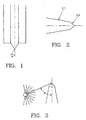
Figure 1 is a diagrammatic illustration of a tapered glass tube; -
Figure 2 is a diagrammatic illustration of a tube tapered during a second tapering cycle; -
Figure 3 illustrates a mechanism for coating a tapered optical fiber; -
Figure 4a illustrates an optical fiber taper for force sensing application; -
Figure 4b illustrates a micropipette taper for force sensing applications; -
Figure 5 illustrates a cantilevered bent fiber tip; -
Figure 6 illustrates a cantilevered pipette constructed in accordance with the invention; -
Figure 7 illustrates a cantilevered pipette used for chemistry; and -
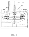
Figure 8 illustrates a device for applying coating to structures. - With pulling technology there are many parameters that can be adjusted to obtain the optimal profile. These are: 1. heat or temperature, 2. the geometric region that is heated, called the filament, 3.the velocity of the pulling that is measured as the glass softens and begins to separate under a constant load and this velocity is determined by the time of heating, 4. the delay between the start of the pulling and turning off the heating element and 5. the tension of the pulling. These can all be microprocessor controlled to develop a geometry in which the glass is first tapered to a dimensionality that is above the cut-off for the propagation of electromagnetic radiation in a metallic waveguide (
Figure 2.1 ) and is then cooled before a second tapering cycle is entered in which a cone angle between 30-40° (Figure 2.2 ) is achieved by multiple pulling cycles. This geometry is shown inFigure 2 . The number of these later cycles depends on the final outer diameter of the tip. - These parameters can be altered in order to tailor the devices for the chemical delivery of materials in nanodimensionalities and to optimize the probes for the dynamic movements of the surfaces of the sample initiated by some external stimulus such as light, sound, electricity etc.
- The above pulling technology can be applied with the following parameters for straight optical fibers in order to get the maximum powers described in this patent.
- For the first taper appropriate parameters would be:
Heat Filament Velocity Delay Pulling 250 3 80 250 10 - For the second taper there is a series of three pulls for a 0.1 micron tip with parameters that could be:
Heat Filament Velocity Delay Pulling 250 0 7 150 10 250 0 10 150 60 290 0 15 126 100 - The coating is accomplished with vacuum deposition of metal. One particular example is a thin chrome coating that is then overcoated with a thicker coating of aluminum. For straight elements this coating is accomplished with an angle of 70° between the normal of the optical element and a line drawn between the tip and the filament (see
Figure 3 ). This angle, a, is crucial for the final dimension of the subwavelength aperture at the tip of this second region of taper. The larger the distance between the filament and the tip the more control of the accuracy of the dimension of the aperture. This occurs because the cotan a approaches the cos of this same angle. - To optimize the force sensing capabilities of these tips the initial taper dimension is chosen to be approximately 20 microns in diameter for region of 100 microns length just above the second taper (see
Figure 4 a) . This is the region in straight fibers that the flexibility of the structure is monitored. This dimensionality controls the resonance frequency and this frequency, f, can be altered up to 500 kHz with a width of the resonance, Δf, that can be 0.75 kHz. - Unlike the etching methodologies, the same pulling technology can be also applied to micropipettes. Such micropipettes have important applications in guiding deep ultraviolet light where optical fibers are not effective. To obtain the optimal parameters we use the following protocol:
Heat Filament Velocity Delay Pulling 390 15 105 200 20 - For the second taper there is a series of three pulls for a 0.1 micron tip with parameters that could be:
Heat Filament Velocity Delay Pulling 220 0 5 200 18 200 0 5 200 15 200 0 30 126 40 - The coating is accomplished with vacuum deposition of metal. One particular example is a thin chrome coating that is then overcoated with a thicker coating of aluminum. For straight elements this coating is accomplished with an angle of 70° between the normal of the optical element and a line drawn between the tip and the filament (see
Figure 3 ). This angle is crucial for the' final dimension of the subwavelength aperture at the tip of this second region of taper. The larger the distance between the filament and the tip the more control of the accuracy of the dimension of the aperture. This occurs because the cotan a approaches the cos of this same angle. - To optimize the force sensing capabilities of these tips the initial taper dimension is chosen to be approximately 25 microns in diameter for region of 100 microns length just above the second taper (see
Figure 4 b) . This is the region in straight tips that the flexibility of the structure is monitored. This dimensionality controls the resonance frequency and this frequency, f, can be altered up to 60 kHz with a width of the resonance, Δf, that can be 0.3 kHz. - Fibers are bent at the tip according to the procedure that is described by K. Lieberman and A. Lewis, "A Method and a Device for Probe Microscopy" [PCT Application Serial Number
PCT/US94/08691 Figure 5 . The angle of the bend in this structure is between 45-60°. The pulling, coating and the resulting resonance frequencies are the same except that the angle of the coating is 85°. In the case of these cantilevered elements such elements can be used for the dynamic sensing of surface movement initiated by an external stimulus such as light, sound, electricity etc. - The pulling and coating parameters are the same as described above for straight pipettes. However, during the bending operation as described in the Lieberman and Lewis patent application [PCT Application Serial Number
PCT/US94/08691 - The structure that is obtained by these pulling parameters is shown in
Figure 6 . This geometric structure is similar in overall characteristics to what has been obtained with a bent fiber. However, the resonance frequencies that can be achieved for this structure are somewhat lower. - In this application a liquid or a gas is transmitted through the narrow opening at the tip of the cantilevered micropipette. Such an uncoated tapered micropipette with force sensing capabilities and a reflective coating only on the cantilever allows the tip to be brought into contact with a surface and this permits the delivery of nanoquantities of material onto the surface. This causes a chemical change on appropriately chosen surfaces if the nature of the chemical in the tip and the chemical in the surface are reactive one with the other.
- In the case of a liquid, under one method of control of the liquid that exists, the tip is accomplished by pressure of the liquid column, by chemical manipulation of the hydrophillicity of the surface and the tip and by the nature of the tip geometry. Specifically on this last parameter the requirement is exactly opposite to what is required for the light funnels tips discussed above. When the surface is appropriately wet by the material in the tip the cone angle of the tip can be as small as 7°. This prevents spreading of the liquid column. Measured resonance frequencies of these structures have been measured at 200 kHz. Additional characteristics that are important in such tips is the need to have high resonance frequencies that will allow for intermittent contact operation and to effectively permit imposed resonances on the tip that will allow, in the case of a liquid chemical in the tip, for the column of liquid to be effectively and reproducibly broken. Another characteristic difference for chemicals exiting the tip that wet surfaces is the angle of the bend and this angle can reach 90° instead of the 60° that is more characteristic of the light funnels (
Fig.7 ) . For other surfaces/tip chemical combinations other angles, tip geometries and resonance frequencies have to be chosen for the most appropriate writing with such tips. Also the force sensing capabilities are of importance in order to give the best sensitivity for measuring the chemical alterations on the surface that have occurred. - The pulling and coating parameters are similar to those that are described in the tips that are used for chemical delivery.
- The pulling and coating parameters are similar to those that are described in the tips that are used for nanodelivery of light since fibers are inserted to illuminate an ion sensing dye filled sol-gel tip from the inside of the micropipette. An additional characteristic is that the tip has to generate sufficient capillary forces to draw a sol-gel into the tip in which there is a dye which changes in optical characteristics with surrounding ion concentration. These sol-gels are conductive to liquid and can be used for both ion conductance and optical ion sensing. It is best that such structures that are to be used in optics are completely coated with metal as is the case in the optical funnels. Materials other than sol-gels can also be used to act as vessels for these dyes.
- Optimization of the force sensing capabilities of the probes described above is achieved by modulating the dimension of the taper of the glass in the region where the flexibility of the structure is monitored and this results in a resonance that is controlled in frequency. By controlling this dimension the frequency, f, can be altered by up to 500 kHz with a width of the resonance, Δf, that can be 0.75 kHz. This allows for maximal response of the tips to dynamic movements of the surface and/or the maximal sensitivity of the tips for the application of non-contact protocols in measuring surface forces.
- To achieve appropriate coatings a device was constructed as shown in
Figure 8 . This device is based on vacuum bell jar and consists of a base 8.1, rotating sealed shaft 8.2, electromotor 8.3, drive gear wheel 8.4 and set of driven gear wheels 8.5 that are mounted on the periphery of a cup 8.6. Rotating mounts 8.7 of tapered straight and/or cantilevered micropipettes and fibers 8.8 are mounted on pillars 8.9 and connected with driven wheel axles by flexible shafts 8.10. - The device operates as following: The motor 8.3 rotates shaft 8.2, which rotates wheel 8.4 and wheels 8.5. Furthermore, the rotary motion is transmitted on mounts 8.7 with fibers 8.8 by shafts 8.10. The angle of the tapered glass elements may be changed by a mount that can be raised and lowered and can turn around on the axle 8.11. So that the rotation of the tapered straight or cantilevered micropipette or fiber during the coating process provides uniformity of deposition, and its rotation provides the opportunity to prevent the coating of the tip itself.
- Techniques are described in this patent that can produce high efficiency throughput of light through tapered glass structures with subwavelength apertures at the tip. Previously, all such attempts at producing such structures were based on etching with chemicals. We have achieved high throughputs by using a series of pulling protocols that permit very high efficiency transmission of light with excellent capabilities for all force sensing protocols. This has never been achieved before. The throughputs that we have achieved permit the generation of ultrasmall spots of light that could extend to below 20 nm with significant intensities of light in these tips. In addition with small amendations these structures can be altered for excellent delivery of nanoquantities of chemicals with nanometric control of chemistry using the force sensing capabilities of these structures and other uses such as combined force and ion sensing etc.
- A variety of applications are envisioned in optics, electronics, chemistry, physics and biology. The structures that have been amended slightly to deliver nanoquantities of chemicals effectively can also be used in a variety of applications where nanometric control of chemistry is required.
Claims (8)
- Use of a micropipette comprised of a tapered glass structure produced from a glass capillary by pulling technologies, the micropipette being bent near a tip to produce a cantilevered structure suitable for normal force sensing in a variety of attractive, repulsive, contact and non-contact modes, the micropipette having an aperture smaller than the wavelength of light, using the force sensing capability of the micropipette and delivering nanoquantities of liquid or gas chemicals for writing on a surface in a controlled fashion so that chemistry can be performed with nanometric control in order to prevent the spreading of the chemicals on the surface.
- Use of a micropipette according to claim 1, wherein chemistry can be performed with nanometric control by pressure on a column of chemicals inside the tapered micropipette, by chemical manipulation of the hydrophillicity of the surface and of the tip, and by the nature of the tapered geometry of the tip and the angle of the cantilever relative to the tip.
- Use of a micropipette according to claim 1 or 2, wherein the micropipette is also adjusted for maximum force sensitivity.
- Use of a micropipette according to any of claims 1 to 3 wherein the force sensing capabilities of the probes are characterized by the dimension of the taper of the glass being appropriately chosen in the region where the flexibility of the structure is monitored to provide a resonance that is controlled in frequency and this frequency, f, can be altered by controlling this dimension up to 500 kHz with a width of the resonance, Δf that can be 0.75 kHz to provide for maximal response of the tips to dynamic movements of the surface and/or application of non-contact protocols in measuring surface forces.
- Use of a micropipette according to any of claims 1 to 4 wherein the micropipette comprises a 0.1 micron tip.
- Use of a micropipette according to any of claims 1 to 5 wherein the micropipette comprises an aperture smaller than the wavelength of deep ultraviolet light.
- Use of a micropipette according to any of claims 1 to 6 wherein the tapered geometry comprises a cone angle of less than 30°.
- Use of a micropipette according to any of claims 1 to 7, wherein the micropipette has resonance frequencies that will allow for intermittent contact operation and will effectively permit imposed resonances on the tip that will allow, in the case of a liquid chemical in the tip, for the column of liquid to be effectively and reproducibly broken.
Applications Claiming Priority (3)
| Application Number | Priority Date | Filing Date | Title |
|---|---|---|---|
| IL12018197A IL120181A0 (en) | 1997-02-09 | 1997-02-09 | Method of producing high throughput tapered straight and cantilevered glass structures for nanodelivery and nanosensing |
| IL12018197 | 1997-02-09 | ||
| PCT/US1998/001577 WO1998037440A2 (en) | 1997-02-09 | 1998-02-09 | Glass structures for nanodelivery and nanosensing |
Publications (3)
| Publication Number | Publication Date |
|---|---|
| EP1023623A2 EP1023623A2 (en) | 2000-08-02 |
| EP1023623A4 EP1023623A4 (en) | 2001-07-25 |
| EP1023623B1 true EP1023623B1 (en) | 2011-07-20 |
Family
ID=11069780
Family Applications (1)
| Application Number | Title | Priority Date | Filing Date |
|---|---|---|---|
| EP98903774A Expired - Lifetime EP1023623B1 (en) | 1997-02-09 | 1998-02-09 | Cantilevered glass structures for nanodelivery of chemicals |
Country Status (3)
| Country | Link |
|---|---|
| EP (1) | EP1023623B1 (en) |
| IL (1) | IL120181A0 (en) |
| WO (1) | WO1998037440A2 (en) |
Families Citing this family (1)
| Publication number | Priority date | Publication date | Assignee | Title |
|---|---|---|---|---|
| JP4620254B2 (en) * | 1999-04-19 | 2011-01-26 | イオンスコープ リミテッド | Light microscopy and its use in cell research |
Family Cites Families (11)
| Publication number | Priority date | Publication date | Assignee | Title |
|---|---|---|---|---|
| US4743548A (en) * | 1984-09-25 | 1988-05-10 | Calgene, Inc. | Plant cell microinjection technique |
| US4917462A (en) | 1988-06-15 | 1990-04-17 | Cornell Research Foundation, Inc. | Near field scanning optical microscopy |
| US4915467A (en) * | 1988-09-12 | 1990-04-10 | Corning Incorporated | Method of making fiber coupler having integral precision connection wells |
| US4877300A (en) * | 1988-10-24 | 1989-10-31 | Corning Incorporated | Non-adiabatically-tapered connector |
| US5044716A (en) * | 1989-12-08 | 1991-09-03 | Corning Incorporated | Chlorine-doped optical component |
| US5015843A (en) * | 1990-02-15 | 1991-05-14 | Polysense, Inc. | Fiber optic chemical sensors based on polymer swelling |
| EP0487233B1 (en) * | 1990-11-19 | 1996-03-20 | AT&T Corp. | Near field scanning optical microscope and applications thereof |
| US5137352A (en) * | 1991-02-05 | 1992-08-11 | Tantec, Inc. | Method and apparatus for determining the contact angle of liquid droplets on curved substrate surfaces |
| US5254854A (en) | 1991-11-04 | 1993-10-19 | At&T Bell Laboratories | Scanning microscope comprising force-sensing means and position-sensitive photodetector |
| IL106613A0 (en) | 1993-08-08 | 1993-12-08 | Klony S Lieberman | Device and method for probe microscopy |
| US9408691B2 (en) | 2013-03-14 | 2016-08-09 | Restoration Robotics, Inc. | Locator device for medical procedures on the body surface and method of its use |
-
1997
- 1997-02-09 IL IL12018197A patent/IL120181A0/en unknown
-
1998
- 1998-02-09 EP EP98903774A patent/EP1023623B1/en not_active Expired - Lifetime
- 1998-02-09 WO PCT/US1998/001577 patent/WO1998037440A2/en not_active Ceased
Also Published As
| Publication number | Publication date |
|---|---|
| WO1998037440A3 (en) | 1998-10-08 |
| EP1023623A4 (en) | 2001-07-25 |
| IL120181A0 (en) | 1997-07-13 |
| EP1023623A2 (en) | 2000-08-02 |
| WO1998037440A2 (en) | 1998-08-27 |
Similar Documents
| Publication | Publication Date | Title |
|---|---|---|
| EP1705475B1 (en) | Optical waveguide probe and its manufacturing method | |
| US5960147A (en) | Probe, manufacturing method therefor and scanning probe microscope | |
| US20080129980A1 (en) | In-line fiber optic sensor devices and methods of fabricating same | |
| EP0664468B1 (en) | Fibre probe having a tip with concave sidewalls | |
| US6580852B2 (en) | Optical fiber probe and cantilever with microscopic aperture, and method of forming microscopic openings | |
| US5677978A (en) | Bent probe microscopy | |
| US5395741A (en) | Method of making fiber probe devices using patterned reactive ion etching | |
| US5986261A (en) | Tapered structure suitable for microthermocouples microelectrodes, field emission tips and micromagnetic sensors with force sensing capabilities | |
| JPH09281123A (en) | Light propagating body probe, scanning near-field microscope, and method for forming transmission holes in light propagating body probe | |
| US6396966B1 (en) | Glass structures for nanodelivery and nanosensing | |
| JP2001165852A (en) | SPR sensor and method of manufacturing the same | |
| US6430324B1 (en) | Optical probe and method for manufacturing same and scanning proximity field optical microscope | |
| Dragnea et al. | Advances in submicron infrared vibrational band chemical imaging | |
| EP0712533B1 (en) | Probe microscopy | |
| JP3825568B2 (en) | PROBE FOR NEAR FIELD LIGHT MICROSCOPE, ITS MANUFACTURING METHOD, AND SCANNER NEAR FIELD LIGHT MICROSCOPE | |
| EP1023623A2 (en) | Producing high throughput tapered straight and cantilevered glass structures for nanodelivery and nanosensing | |
| WO1998037440A9 (en) | Glass structures for nanodelivery and nanosensing | |
| JP4778616B2 (en) | Optical fiber and unique micropipette with lens with subwavelength aperture | |
| US5812722A (en) | Optical fiber and method for manufacturing the same | |
| JP4183684B2 (en) | Probe for near-field optical microscope and manufacturing method thereof | |
| US6600856B1 (en) | Lensed optical fibers and unique micropipettes with subwavelength apertures | |
| US20050214452A1 (en) | Method and apparatus for depositing material with high resolution | |
| JP3023048B2 (en) | Optical fiber probe and method of manufacturing the same | |
| EP0839383B1 (en) | Tapered structure suitable for microthermocouples microelectrodes, field emission tips and micromagnetic sensors with force sensing capabilities | |
| JP3764816B2 (en) | Flamingo optical probe, flamingo optical probe manufacturing method, and scanning probe microscope |
Legal Events
| Date | Code | Title | Description |
|---|---|---|---|
| PUAI | Public reference made under article 153(3) epc to a published international application that has entered the european phase |
Free format text: ORIGINAL CODE: 0009012 |
|
| 17P | Request for examination filed |
Effective date: 19990903 |
|
| AK | Designated contracting states |
Kind code of ref document: A2 Designated state(s): CH DE FR GB LI |
|
| RIC1 | Information provided on ipc code assigned before grant |
Free format text: 7G 02B 21/00 A, 7B 01L 3/02 B |
|
| A4 | Supplementary search report drawn up and despatched |
Effective date: 20010608 |
|
| AK | Designated contracting states |
Kind code of ref document: A4 Designated state(s): CH DE FR GB LI |
|
| RA4 | Supplementary search report drawn up and despatched (corrected) |
Effective date: 20010622 |
|
| APBN | Date of receipt of notice of appeal recorded |
Free format text: ORIGINAL CODE: EPIDOSNNOA2E |
|
| APBR | Date of receipt of statement of grounds of appeal recorded |
Free format text: ORIGINAL CODE: EPIDOSNNOA3E |
|
| APAF | Appeal reference modified |
Free format text: ORIGINAL CODE: EPIDOSCREFNE |
|
| APBT | Appeal procedure closed |
Free format text: ORIGINAL CODE: EPIDOSNNOA9E |
|
| GRAP | Despatch of communication of intention to grant a patent |
Free format text: ORIGINAL CODE: EPIDOSNIGR1 |
|
| RIC1 | Information provided on ipc code assigned before grant |
Ipc: G01Q 60/18 20100101AFI20100126BHEP |
|
| RTI1 | Title (correction) |
Free format text: CANTILEVERED GLASS STRUCTURES FOR NANODELIVERY OF CHEMICALS |
|
| RTI1 | Title (correction) |
Free format text: CANTILEVERED GLASS STRUCTURES FOR NANODELIVERY OF CHEMICALS |
|
| GRAS | Grant fee paid |
Free format text: ORIGINAL CODE: EPIDOSNIGR3 |
|
| GRAA | (expected) grant |
Free format text: ORIGINAL CODE: 0009210 |
|
| AK | Designated contracting states |
Kind code of ref document: B1 Designated state(s): CH DE FR GB LI |
|
| REG | Reference to a national code |
Ref country code: GB Ref legal event code: FG4D |
|
| REG | Reference to a national code |
Ref country code: CH Ref legal event code: EP |
|
| REG | Reference to a national code |
Ref country code: DE Ref legal event code: R096 Ref document number: 69842340 Country of ref document: DE Effective date: 20110915 |
|
| PLBE | No opposition filed within time limit |
Free format text: ORIGINAL CODE: 0009261 |
|
| STAA | Information on the status of an ep patent application or granted ep patent |
Free format text: STATUS: NO OPPOSITION FILED WITHIN TIME LIMIT |
|
| 26N | No opposition filed |
Effective date: 20120423 |
|
| REG | Reference to a national code |
Ref country code: DE Ref legal event code: R097 Ref document number: 69842340 Country of ref document: DE Effective date: 20120423 |
|
| REG | Reference to a national code |
Ref country code: CH Ref legal event code: PL |
|
| GBPC | Gb: european patent ceased through non-payment of renewal fee |
Effective date: 20120209 |
|
| PG25 | Lapsed in a contracting state [announced via postgrant information from national office to epo] |
Ref country code: LI Free format text: LAPSE BECAUSE OF NON-PAYMENT OF DUE FEES Effective date: 20120229 Ref country code: CH Free format text: LAPSE BECAUSE OF NON-PAYMENT OF DUE FEES Effective date: 20120229 |
|
| REG | Reference to a national code |
Ref country code: FR Ref legal event code: ST Effective date: 20121031 |
|
| REG | Reference to a national code |
Ref country code: DE Ref legal event code: R119 Ref document number: 69842340 Country of ref document: DE Effective date: 20120901 |
|
| PG25 | Lapsed in a contracting state [announced via postgrant information from national office to epo] |
Ref country code: FR Free format text: LAPSE BECAUSE OF NON-PAYMENT OF DUE FEES Effective date: 20120229 Ref country code: GB Free format text: LAPSE BECAUSE OF NON-PAYMENT OF DUE FEES Effective date: 20120209 |
|
| PG25 | Lapsed in a contracting state [announced via postgrant information from national office to epo] |
Ref country code: DE Free format text: LAPSE BECAUSE OF NON-PAYMENT OF DUE FEES Effective date: 20120901 |