EP1021679B1 - Sight for weapons - Google Patents
Sight for weapons Download PDFInfo
- Publication number
- EP1021679B1 EP1021679B1 EP98948049A EP98948049A EP1021679B1 EP 1021679 B1 EP1021679 B1 EP 1021679B1 EP 98948049 A EP98948049 A EP 98948049A EP 98948049 A EP98948049 A EP 98948049A EP 1021679 B1 EP1021679 B1 EP 1021679B1
- Authority
- EP
- European Patent Office
- Prior art keywords
- light emitting
- mask
- light
- diode element
- sight
- Prior art date
- Legal status (The legal status is an assumption and is not a legal conclusion. Google has not performed a legal analysis and makes no representation as to the accuracy of the status listed.)
- Expired - Lifetime
Links
- 239000006185 dispersion Substances 0.000 claims abstract description 7
- 238000001228 spectrum Methods 0.000 claims description 2
- 239000004020 conductor Substances 0.000 claims 1
- 230000001681 protective effect Effects 0.000 claims 1
- 230000003287 optical effect Effects 0.000 description 6
- NIOPZPCMRQGZCE-WEVVVXLNSA-N 2,4-dinitro-6-(octan-2-yl)phenyl (E)-but-2-enoate Chemical compound CCCCCCC(C)C1=CC([N+]([O-])=O)=CC([N+]([O-])=O)=C1OC(=O)\C=C\C NIOPZPCMRQGZCE-WEVVVXLNSA-N 0.000 description 5
- PCHJSUWPFVWCPO-UHFFFAOYSA-N gold Chemical compound [Au] PCHJSUWPFVWCPO-UHFFFAOYSA-N 0.000 description 3
- 239000010931 gold Substances 0.000 description 3
- 229910052737 gold Inorganic materials 0.000 description 3
- 239000000463 material Substances 0.000 description 3
- 239000004411 aluminium Substances 0.000 description 2
- 229910052782 aluminium Inorganic materials 0.000 description 2
- XAGFODPZIPBFFR-UHFFFAOYSA-N aluminium Chemical compound [Al] XAGFODPZIPBFFR-UHFFFAOYSA-N 0.000 description 2
- 239000011248 coating agent Substances 0.000 description 2
- 238000000576 coating method Methods 0.000 description 2
- 229910052751 metal Inorganic materials 0.000 description 2
- 239000002184 metal Substances 0.000 description 2
- 238000000034 method Methods 0.000 description 2
- 239000004593 Epoxy Substances 0.000 description 1
- 239000000919 ceramic Substances 0.000 description 1
- 230000003247 decreasing effect Effects 0.000 description 1
- 238000010304 firing Methods 0.000 description 1
- 239000003365 glass fiber Substances 0.000 description 1
Images

Classifications
-
- G—PHYSICS
- G02—OPTICS
- G02B—OPTICAL ELEMENTS, SYSTEMS OR APPARATUS
- G02B23/00—Telescopes, e.g. binoculars; Periscopes; Instruments for viewing the inside of hollow bodies; Viewfinders; Optical aiming or sighting devices
- G02B23/02—Telescopes, e.g. binoculars; Periscopes; Instruments for viewing the inside of hollow bodies; Viewfinders; Optical aiming or sighting devices involving prisms or mirrors
- G02B23/10—Telescopes, e.g. binoculars; Periscopes; Instruments for viewing the inside of hollow bodies; Viewfinders; Optical aiming or sighting devices involving prisms or mirrors reflecting into the field of view additional indications, e.g. from collimator
-
- F—MECHANICAL ENGINEERING; LIGHTING; HEATING; WEAPONS; BLASTING
- F41—WEAPONS
- F41G—WEAPON SIGHTS; AIMING
- F41G1/00—Sighting devices
- F41G1/32—Night sights, e.g. luminescent
- F41G1/34—Night sights, e.g. luminescent combined with light source, e.g. spot light
- F41G1/36—Night sights, e.g. luminescent combined with light source, e.g. spot light with infrared light source
-
- G—PHYSICS
- G02—OPTICS
- G02B—OPTICAL ELEMENTS, SYSTEMS OR APPARATUS
- G02B27/00—Optical systems or apparatus not provided for by any of the groups G02B1/00 - G02B26/00, G02B30/00
- G02B27/18—Optical systems or apparatus not provided for by any of the groups G02B1/00 - G02B26/00, G02B30/00 for optical projection, e.g. combination of mirror and condenser and objective
- G02B27/20—Optical systems or apparatus not provided for by any of the groups G02B1/00 - G02B26/00, G02B30/00 for optical projection, e.g. combination of mirror and condenser and objective for imaging minute objects, e.g. light-pointer
-
- Y—GENERAL TAGGING OF NEW TECHNOLOGICAL DEVELOPMENTS; GENERAL TAGGING OF CROSS-SECTIONAL TECHNOLOGIES SPANNING OVER SEVERAL SECTIONS OF THE IPC; TECHNICAL SUBJECTS COVERED BY FORMER USPC CROSS-REFERENCE ART COLLECTIONS [XRACs] AND DIGESTS
- Y10—TECHNICAL SUBJECTS COVERED BY FORMER USPC
- Y10S—TECHNICAL SUBJECTS COVERED BY FORMER USPC CROSS-REFERENCE ART COLLECTIONS [XRACs] AND DIGESTS
- Y10S362/00—Illumination
- Y10S362/80—Light emitting diode
Definitions
- the present invention relates to a light emitting device, preferably a light emitting diode device, providing a light beam with limited dispersion.
- the device is particularly, but not exclusively, intended for use in a so called red dot sight mounted on a weapon.
- the red dot is projected on a lens as an aiming point, the gunner looking through the lens when aiming.
- a battery powered light emitting diode (LED)
- the LED shall provide a narrow and distinct beam of light, which - as appears from the name of the device - may be red.
- the shape of the beam may vary but is most often circular, so that a red dot appears for the gunner in the sight.
- the beam is created by placing a mask with a narrow hole at the end of the plastic bulb of the LED.
- the normally desired circular beam is created by a circular hole.
- the mask Due to the presence of the bulb the mask will be at a certain distance from the light emitting surface of the LED, for example 2 mm or more. As the light dispersion increases with the square of the distance, the efficiency of the device is not satisfactory, which in turn means that the battery power will be consumed comparatively quickly.
- Another problem in the conventional sight is that the intensity of the projected light varies when looking at different areas of the surface of the lens.
- the main object of the invention is to remove the above stated drawbacks and to attain a light emitting device which is more efficient in providing a light beam with limited dispersion and which allows that the light emitting surface of the LED always covers the whole pattern of the mask.
- a light-impermeable mask with a hole for light is arranged on or in direct vicinity to a light emitting surface of a light emitting element in the device.
- the diode current may be decreased by a factor of 5 - 10, resulting in a corresponding increase of the battery life.
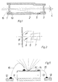
- Fig 1 is a schematic longitudinal section through a sight with a light emitting device.
- Fig 2 is a side view of a prior art light emitting device.
- Fig 3 is a top view of a light emitting device according to the invention,
- Fig 4 is a section along the line IV-IV in Fig 3, and
- Fig 5 is a section through a light emitting device according to the invention and serves to illustrate a special feature of the invention.
- the sight shown in Fig 1 serves only the purpose of exemplifying a use of the light emitting device according to the invention.
- This sight has an optical element 1, such as a lens, which is attached to the forward end of a light channel shaped as a tube 2.
- This tube has a circular cross section.
- the diameter of the optical element may be for example 35 mm.
- a transparent window 3 is attached, which is directed towards the eye 4 of the gunner using a weapon (not shown) on which the sight is mounted.
- the optical element 1 comprises a lens having a concave side directed towards the transparent window 3, and a convex opposite side.
- the concave side is spherically or parabolically shaped.
- the focal point of the optical element 1 falls inside the light channel below its center line.
- a light emitting device preferably a light emitting diode (LED) 5
- LED light emitting diode
- the inner surface of the element 1 is coated with a partially reflecting layer 1a, which is reflective to light in a certain defined wave length interval, for example around the wave length 630 nm, i e red light only, while light of all other wave lengths passes through the element substantially without reflection, said wave length being chosen in dependence of the wave length of the light emitted from the LED 5.
- a partially reflecting layer 1a which is reflective to light in a certain defined wave length interval, for example around the wave length 630 nm, i e red light only, while light of all other wave lengths passes through the element substantially without reflection, said wave length being chosen in dependence of the wave length of the light emitted from the LED 5.
- the convex side of the element 1 is coated with an anti-reflecting layer 1b, a so called AR-coating, in order to avoid reflections from this side of the optical element and especially from the LED 5. If the optical element 1 consists of more than one lens the coating could preferable be on the convex side of the inner lens.
- the gunner's eye 4 will see a red aiming point superimposed on the image of the surroundings or the target when looking through the sight. Provided that the sight is properly mounted on the weapon, the gunner only has to place the red aiming point on the target to be able to hit it when firing the weapon.
- a conventional LED is rather schematically illustrated in Fig 2.
- a light emitting element 6 is arranged on a base 7.
- a plastic casing 8 is mounted on the base 7 over the element 6 and may have the shown shape in order to properly direct the light from the element 6.
- a mask 9 with an opening 9' is placed over the end of the casing 8 in order to define the shape of the aiming point and mask off undesired light.
- the opening 9' is circular (for obtaining an aiming point in the form af a dot) and may for example have a diameter of 0.06 mm.
- the distance between the light emitting surface of the element 6 and the mask 9 may be of the order of 2 mm. Taking into account that the light dispersion is proportional to the square of this distance, it is obvious that the efficiency is not satisfactory.
- a light emitting device has the following design, reference being made to Figs 3 and 4.
- an electrically non-conducting base plate 10 there are arranged an electrode 11 and a second electrode 12 of for example gold or aluminium or any other suitable metal. They may be shaped as shown in Fig 3 to be suitably close to each other.
- a light emitting diode element 13 with planar surfaces is arranged at the end of the anode 11.
- the material used for the element 13 is conventional per se. It may for example be GaAlAs for obtaining light emission in the red part of the spectrum (620 - 690 nm), GaP for the green part (540 - 570 nm) or SiC for the blue part (440 - 480 nm). It is preferred that the element 13 has a light intensity of at least 10 mcd at a current of 20 mA.
- a mask 14 with a hole 14' which for example may be circular for obtaining a circular light beam, is arranged directly on top of the diode element 13.
- This mask 14 may be made for example of gold or another metal and have a thickness of the order of 1 to 5 ⁇ m. It may be vaporized or sputtered directly on the element 13. Alternatively, it may be glued or painted thereto. As in the prior art device described with reference to Fig 2, the hole 14' may have a diameter of 0.06 mm.
- Bonding threads 15 of gold, aluminium or any other suitable material are arranged to connect the cathode 12 with the upper side of the mask 14. These threads may have a diameter of the order of 5 ⁇ m. The bonding itself will be described below with reference to Fig 5.
- the described light emitting device 10 - 15 may be arranged in an opening in a top plate 16 connected to or integral with the base plate 10.
- the material in the plates 10, 16 may be glass fiber reinforced epoxy or ceramic.
- the opening in the top plate 16 is filled with an opaque mass 17 of black ink protecting the device against leakage of unwanted light and mechanical stress but leaving the hole 14' in the mask 14 unobstructed, so that a light beam can be emitted therethrough when the device is operated.
- the light emitting device is shown to a larger scale in Fig 5, which serves to illustrate a conventional bonding method to the left and a new and improved method to the right.
- the bonding thread 15 is connected substantially perpendicularly to both the electrode 12 and the mask 14, so that the bow-shaped thread may obstruct the light beam leaving the hole 14', as is illustrated to the left in Fig 5.
- the bonding thread 15 may be bonded substantially parallel with the surface of the mask 14 by means of a so called wedge bonding, as is illustrated to the right in Fig 5.
Landscapes
- Physics & Mathematics (AREA)
- Optics & Photonics (AREA)
- General Physics & Mathematics (AREA)
- Astronomy & Astrophysics (AREA)
- Engineering & Computer Science (AREA)
- General Engineering & Computer Science (AREA)
- Led Device Packages (AREA)
- Led Devices (AREA)
- Vehicle Step Arrangements And Article Storage (AREA)
- Gloves (AREA)
- Rear-View Mirror Devices That Are Mounted On The Exterior Of The Vehicle (AREA)
- Organic Low-Molecular-Weight Compounds And Preparation Thereof (AREA)
- Illuminated Signs And Luminous Advertising (AREA)
Abstract
Description
Claims (10)
- A light emitting device, preferably a light emitting diode device, providing a light beam with limited dispersion, characterized in that a light-impermeable mask (14) with a hole (14') for light is arranged on or in direct vicinity to a light emitting surface of a light emitting element (13) in the device.
- A device according to claim 1, wherein the light beam is projected towards a lens, characterized in that the light emitting surface of the light emitting element (13) covers the whole pattern of the mask as viewed from all angles defined by the lens.
- A device according to claim 1 or 2, characterized by the use of a light emitting diode element (13) with a planar light emitting surface, on which the mask (14) is arranged.
- A device according to claim 3, characterized in that the diode element (13) is of GaAlAs for light emission in the red part of the spectrum (620 - 690 nm), GaP for the green part (540 - 570 nm) or SiC for the blue part (440 - 480 nm).
- A device according to claim 3, characterized in that the mask (14) is vaporized or sputtered on the diode element (13).
- A device according to claim 3, characterized in that the mask (14) is glued or painted on the diode element (13).
- A device according to claim 3, characterized in that an electrode (11), the light emitting diode element (13), and the mask (14) of an electrically conducting material are arranged on top of each other as a unit and that bonding threads (15) extend from the electrodes (12) to the free surface of the mask.
- A device according to claim 7, characterized in that it is embedded in a protective opaque mass (17) with the mask hole (14') left unobstructed for light emission.
- A device according to claim 7, characterized in that the bonding threads (15) are bonded substantially parallel to the free surface of the mask (14).
- A device according to any of the preceding claims, characterized by its use in a sight for a weapon or similar equipment.
Applications Claiming Priority (3)
| Application Number | Priority Date | Filing Date | Title |
|---|---|---|---|
| SE9703683A SE512276C2 (en) | 1997-10-09 | 1997-10-09 | Light emitting device |
| SE9703683 | 1997-10-09 | ||
| PCT/SE1998/001814 WO1999019665A1 (en) | 1997-10-09 | 1998-10-08 | Sight for weapons |
Publications (2)
| Publication Number | Publication Date |
|---|---|
| EP1021679A1 EP1021679A1 (en) | 2000-07-26 |
| EP1021679B1 true EP1021679B1 (en) | 2002-04-10 |
Family
ID=20408554
Family Applications (1)
| Application Number | Title | Priority Date | Filing Date |
|---|---|---|---|
| EP98948049A Expired - Lifetime EP1021679B1 (en) | 1997-10-09 | 1998-10-08 | Sight for weapons |
Country Status (9)
| Country | Link |
|---|---|
| US (1) | US6601966B1 (en) |
| EP (1) | EP1021679B1 (en) |
| JP (1) | JP4493841B2 (en) |
| AT (1) | ATE216049T1 (en) |
| AU (1) | AU9470598A (en) |
| CA (1) | CA2306556C (en) |
| DE (1) | DE69804835T2 (en) |
| SE (1) | SE512276C2 (en) |
| WO (1) | WO1999019665A1 (en) |
Families Citing this family (12)
| Publication number | Priority date | Publication date | Assignee | Title |
|---|---|---|---|---|
| SE518587C2 (en) * | 2001-01-09 | 2002-10-29 | Gs Dev Ab | Optical sight |
| SE524172C2 (en) | 2002-06-24 | 2004-07-06 | Gs Dev Ab | weapon sight |
| US7325354B2 (en) * | 2004-05-06 | 2008-02-05 | Insight Technology, Inc. | Weapon aiming device |
| US8215024B1 (en) | 2006-04-15 | 2012-07-10 | Michael Terzo | Sighting device for a weapon |
| JP4585532B2 (en) * | 2007-02-23 | 2010-11-24 | 東芝電波プロダクツ株式会社 | Dat site |
| SE533391C2 (en) | 2008-05-09 | 2010-09-14 | Gs Dev Ab | combination sight |
| JP5537295B2 (en) * | 2010-07-05 | 2014-07-02 | パナソニック株式会社 | Light emitting element mounting wiring pattern, light emitting element mounting wiring board having light emitting element mounting wiring pattern, light emitting module using light emitting element mounting wiring board, and lighting fixture equipped with light emitting module |
| US10690325B2 (en) | 2013-05-13 | 2020-06-23 | Riverpoint Medical, Llc | Medical headlamp optical arrangement permitting variable beam width |
| US9687314B2 (en) | 2013-05-13 | 2017-06-27 | Riverpoint Medical, Llc | Medical headlamp optical arrangement |
| JP2018180270A (en) * | 2017-04-13 | 2018-11-15 | 株式会社東京スコープ | Dot site |
| US10634330B1 (en) | 2017-10-31 | 2020-04-28 | Riverpoint Medical, Llc | Headband assembly |
| US11287638B2 (en) | 2019-08-20 | 2022-03-29 | Francesco E. DeAngelis | Reflex sight with superluminescent micro-display, dynamic reticle, and metadata overlay |
Family Cites Families (12)
| Publication number | Priority date | Publication date | Assignee | Title |
|---|---|---|---|---|
| US3886396A (en) * | 1971-10-10 | 1975-05-27 | Gen Electric | Fluorescent lamp with protective coating |
| JPS6374994U (en) * | 1986-10-31 | 1988-05-18 | ||
| US4967330A (en) | 1990-03-16 | 1990-10-30 | Bell Howard F | LED lamp with open encasement |
| US5068969A (en) * | 1990-04-09 | 1991-12-03 | Siebert Robert M | Lighted gun sight |
| US5119174A (en) * | 1990-10-26 | 1992-06-02 | Chen Der Jong | Light emitting diode display with PCB base |
| US5272514A (en) * | 1991-12-06 | 1993-12-21 | Litton Systems, Inc. | Modular day/night weapon aiming system |
| DE4308864C2 (en) | 1992-06-25 | 1996-05-09 | Agfa Gevaert Ag | Device for copying transparent image templates |
| JPH0651129A (en) * | 1992-07-27 | 1994-02-25 | Inoue Denki Kk | Illuminating device |
| JPH06291365A (en) * | 1993-03-30 | 1994-10-18 | Omron Corp | Semiconductor light emitting device and its manufacturing method, optical detecting device, optical information processing device, and optical fiber module |
| JPH0736388A (en) * | 1993-07-16 | 1995-02-07 | Tanaka Kikinzoku Kogyo Kk | Light diffusion prevention mask for LED display |
| US5642149A (en) | 1993-09-20 | 1997-06-24 | Eastman Kodak Company | Apparatus and method for printing with a non-refractive imaging system |
| US5463502A (en) * | 1994-05-16 | 1995-10-31 | Savage, Jr.; John M. | Lens assembly for use with LEDs |
-
1997
- 1997-10-09 SE SE9703683A patent/SE512276C2/en not_active IP Right Cessation
-
1998
- 1998-10-08 AU AU94705/98A patent/AU9470598A/en not_active Abandoned
- 1998-10-08 CA CA002306556A patent/CA2306556C/en not_active Expired - Lifetime
- 1998-10-08 JP JP2000516183A patent/JP4493841B2/en not_active Expired - Lifetime
- 1998-10-08 DE DE69804835T patent/DE69804835T2/en not_active Expired - Lifetime
- 1998-10-08 AT AT98948049T patent/ATE216049T1/en not_active IP Right Cessation
- 1998-10-08 EP EP98948049A patent/EP1021679B1/en not_active Expired - Lifetime
- 1998-10-08 WO PCT/SE1998/001814 patent/WO1999019665A1/en not_active Ceased
- 1998-10-08 US US09/529,147 patent/US6601966B1/en not_active Expired - Lifetime
Also Published As
| Publication number | Publication date |
|---|---|
| SE512276C2 (en) | 2000-02-21 |
| JP4493841B2 (en) | 2010-06-30 |
| US6601966B1 (en) | 2003-08-05 |
| EP1021679A1 (en) | 2000-07-26 |
| CA2306556C (en) | 2007-06-05 |
| AU9470598A (en) | 1999-05-03 |
| JP2001520359A (en) | 2001-10-30 |
| ATE216049T1 (en) | 2002-04-15 |
| DE69804835D1 (en) | 2002-05-16 |
| CA2306556A1 (en) | 1999-04-22 |
| SE9703683L (en) | 1999-04-10 |
| DE69804835T2 (en) | 2002-10-10 |
| WO1999019665A1 (en) | 1999-04-22 |
Similar Documents
| Publication | Publication Date | Title |
|---|---|---|
| CA2306556C (en) | Sight for weapons | |
| US6216352B1 (en) | Day/night weapon sight | |
| US7627976B1 (en) | Fiber optic sight for firearms with nighttime capabilities | |
| EP1161650B1 (en) | Day/night weapon sight | |
| US5653034A (en) | Reflex sighting device for day and night sighting | |
| US6571482B1 (en) | Sighting device for projectile type weapons for operation in day and night | |
| US7562486B2 (en) | Self-illuminated sighting device | |
| US5016152A (en) | Focused light source and method | |
| US20070107292A1 (en) | Retro-reflective aiming means | |
| US8189967B1 (en) | Fiber optic sight for firearms | |
| JPS60182406A (en) | Sight device | |
| GB2292465A (en) | Optical sight with part-reflective aspheric surface and mount | |
| US5044748A (en) | Collimator gun sight | |
| US3218718A (en) | Sighting system for firearms | |
| EP1350072B1 (en) | Optical sight | |
| CA3244901A1 (en) | Reticle for a viewing optic | |
| US3937968A (en) | Optical aiming device employing radioluminous material | |
| US11719510B2 (en) | Light dot sight | |
| US7025484B2 (en) | Light source | |
| CN121477496A (en) | A high-brightness reticle illumination mechanism and a sight having the same. | |
| CN121953732A (en) | Multi-mode differentiated graph lighting system and device of sighting telescope | |
| HU183634B (en) | Improved radioluminescent light source |
Legal Events
| Date | Code | Title | Description |
|---|---|---|---|
| PUAI | Public reference made under article 153(3) epc to a published international application that has entered the european phase |
Free format text: ORIGINAL CODE: 0009012 |
|
| 17P | Request for examination filed |
Effective date: 20000414 |
|
| AK | Designated contracting states |
Kind code of ref document: A1 Designated state(s): AT BE CH CY DE DK ES FI FR GB GR IE IT LI LU MC NL PT SE |
|
| GRAG | Despatch of communication of intention to grant |
Free format text: ORIGINAL CODE: EPIDOS AGRA |
|
| 17Q | First examination report despatched |
Effective date: 20010528 |
|
| GRAG | Despatch of communication of intention to grant |
Free format text: ORIGINAL CODE: EPIDOS AGRA |
|
| GRAH | Despatch of communication of intention to grant a patent |
Free format text: ORIGINAL CODE: EPIDOS IGRA |
|
| REG | Reference to a national code |
Ref country code: GB Ref legal event code: IF02 |
|
| GRAH | Despatch of communication of intention to grant a patent |
Free format text: ORIGINAL CODE: EPIDOS IGRA |
|
| GRAA | (expected) grant |
Free format text: ORIGINAL CODE: 0009210 |
|
| AK | Designated contracting states |
Kind code of ref document: B1 Designated state(s): AT BE CH CY DE DK ES FI FR GB GR IE IT LI LU MC NL PT SE |
|
| PG25 | Lapsed in a contracting state [announced via postgrant information from national office to epo] |
Ref country code: NL Free format text: LAPSE BECAUSE OF FAILURE TO SUBMIT A TRANSLATION OF THE DESCRIPTION OR TO PAY THE FEE WITHIN THE PRESCRIBED TIME-LIMIT Effective date: 20020410 Ref country code: LI Free format text: LAPSE BECAUSE OF FAILURE TO SUBMIT A TRANSLATION OF THE DESCRIPTION OR TO PAY THE FEE WITHIN THE PRESCRIBED TIME-LIMIT Effective date: 20020410 Ref country code: GR Free format text: LAPSE BECAUSE OF FAILURE TO SUBMIT A TRANSLATION OF THE DESCRIPTION OR TO PAY THE FEE WITHIN THE PRESCRIBED TIME-LIMIT Effective date: 20020410 Ref country code: FI Free format text: LAPSE BECAUSE OF FAILURE TO SUBMIT A TRANSLATION OF THE DESCRIPTION OR TO PAY THE FEE WITHIN THE PRESCRIBED TIME-LIMIT Effective date: 20020410 Ref country code: CH Free format text: LAPSE BECAUSE OF FAILURE TO SUBMIT A TRANSLATION OF THE DESCRIPTION OR TO PAY THE FEE WITHIN THE PRESCRIBED TIME-LIMIT Effective date: 20020410 Ref country code: BE Free format text: LAPSE BECAUSE OF FAILURE TO SUBMIT A TRANSLATION OF THE DESCRIPTION OR TO PAY THE FEE WITHIN THE PRESCRIBED TIME-LIMIT Effective date: 20020410 Ref country code: AT Free format text: LAPSE BECAUSE OF FAILURE TO SUBMIT A TRANSLATION OF THE DESCRIPTION OR TO PAY THE FEE WITHIN THE PRESCRIBED TIME-LIMIT Effective date: 20020410 |
|
| REF | Corresponds to: |
Ref document number: 216049 Country of ref document: AT Date of ref document: 20020415 Kind code of ref document: T |
|
| REG | Reference to a national code |
Ref country code: CH Ref legal event code: EP |
|
| REG | Reference to a national code |
Ref country code: IE Ref legal event code: FG4D |
|
| REF | Corresponds to: |
Ref document number: 69804835 Country of ref document: DE Date of ref document: 20020516 |
|
| PG25 | Lapsed in a contracting state [announced via postgrant information from national office to epo] |
Ref country code: SE Free format text: LAPSE BECAUSE OF FAILURE TO SUBMIT A TRANSLATION OF THE DESCRIPTION OR TO PAY THE FEE WITHIN THE PRESCRIBED TIME-LIMIT Effective date: 20020710 Ref country code: PT Free format text: LAPSE BECAUSE OF FAILURE TO SUBMIT A TRANSLATION OF THE DESCRIPTION OR TO PAY THE FEE WITHIN THE PRESCRIBED TIME-LIMIT Effective date: 20020710 Ref country code: DK Free format text: LAPSE BECAUSE OF FAILURE TO SUBMIT A TRANSLATION OF THE DESCRIPTION OR TO PAY THE FEE WITHIN THE PRESCRIBED TIME-LIMIT Effective date: 20020710 |
|
| NLV1 | Nl: lapsed or annulled due to failure to fulfill the requirements of art. 29p and 29m of the patents act | ||
| ET | Fr: translation filed | ||
| PG25 | Lapsed in a contracting state [announced via postgrant information from national office to epo] |
Ref country code: LU Free format text: LAPSE BECAUSE OF NON-PAYMENT OF DUE FEES Effective date: 20021008 Ref country code: IE Free format text: LAPSE BECAUSE OF NON-PAYMENT OF DUE FEES Effective date: 20021008 |
|
| REG | Reference to a national code |
Ref country code: CH Ref legal event code: PL |
|
| PG25 | Lapsed in a contracting state [announced via postgrant information from national office to epo] |
Ref country code: ES Free format text: LAPSE BECAUSE OF FAILURE TO SUBMIT A TRANSLATION OF THE DESCRIPTION OR TO PAY THE FEE WITHIN THE PRESCRIBED TIME-LIMIT Effective date: 20021030 |
|
| PG25 | Lapsed in a contracting state [announced via postgrant information from national office to epo] |
Ref country code: CY Free format text: LAPSE BECAUSE OF FAILURE TO SUBMIT A TRANSLATION OF THE DESCRIPTION OR TO PAY THE FEE WITHIN THE PRESCRIBED TIME-LIMIT Effective date: 20021031 |
|
| PLBE | No opposition filed within time limit |
Free format text: ORIGINAL CODE: 0009261 |
|
| STAA | Information on the status of an ep patent application or granted ep patent |
Free format text: STATUS: NO OPPOSITION FILED WITHIN TIME LIMIT |
|
| 26N | No opposition filed |
Effective date: 20030113 |
|
| PG25 | Lapsed in a contracting state [announced via postgrant information from national office to epo] |
Ref country code: MC Free format text: LAPSE BECAUSE OF NON-PAYMENT OF DUE FEES Effective date: 20030501 |
|
| REG | Reference to a national code |
Ref country code: IE Ref legal event code: MM4A |
|
| PGFP | Annual fee paid to national office [announced via postgrant information from national office to epo] |
Ref country code: IT Payment date: 20061031 Year of fee payment: 9 |
|
| PG25 | Lapsed in a contracting state [announced via postgrant information from national office to epo] |
Ref country code: IT Free format text: LAPSE BECAUSE OF NON-PAYMENT OF DUE FEES Effective date: 20071008 |
|
| REG | Reference to a national code |
Ref country code: FR Ref legal event code: PLFP Year of fee payment: 18 |
|
| REG | Reference to a national code |
Ref country code: GB Ref legal event code: 732E Free format text: REGISTERED BETWEEN 20160512 AND 20160518 |
|
| REG | Reference to a national code |
Ref country code: DE Ref legal event code: R082 Ref document number: 69804835 Country of ref document: DE Representative=s name: KLUNKER IP PATENTANWAELTE PARTG MBB, DE Ref country code: DE Ref legal event code: R082 Ref document number: 69804835 Country of ref document: DE Representative=s name: KLUNKER, SCHMITT-NILSON, HIRSCH, DE Ref country code: DE Ref legal event code: R081 Ref document number: 69804835 Country of ref document: DE Owner name: AIMPOINT AB, SE Free format text: FORMER OWNER: GS DEVELOPMENT AB, MALMOE, SE |
|
| REG | Reference to a national code |
Ref country code: FR Ref legal event code: TP Owner name: AIMPOINT AB, SE Effective date: 20160629 |
|
| REG | Reference to a national code |
Ref country code: FR Ref legal event code: PLFP Year of fee payment: 19 |
|
| REG | Reference to a national code |
Ref country code: DE Ref legal event code: R082 Ref document number: 69804835 Country of ref document: DE Representative=s name: KLUNKER IP PATENTANWAELTE PARTG MBB, DE |
|
| REG | Reference to a national code |
Ref country code: FR Ref legal event code: PLFP Year of fee payment: 20 |
|
| PGFP | Annual fee paid to national office [announced via postgrant information from national office to epo] |
Ref country code: DE Payment date: 20171010 Year of fee payment: 20 Ref country code: FR Payment date: 20171031 Year of fee payment: 20 |
|
| PGFP | Annual fee paid to national office [announced via postgrant information from national office to epo] |
Ref country code: GB Payment date: 20171016 Year of fee payment: 20 |
|
| REG | Reference to a national code |
Ref country code: DE Ref legal event code: R071 Ref document number: 69804835 Country of ref document: DE |
|
| REG | Reference to a national code |
Ref country code: GB Ref legal event code: PE20 Expiry date: 20181007 |
|
| PG25 | Lapsed in a contracting state [announced via postgrant information from national office to epo] |
Ref country code: GB Free format text: LAPSE BECAUSE OF EXPIRATION OF PROTECTION Effective date: 20181007 |
|
| P01 | Opt-out of the competence of the unified patent court (upc) registered |
Effective date: 20230530 |