EP1020980A2 - Switching power supply unit - Google Patents
Switching power supply unit Download PDFInfo
- Publication number
- EP1020980A2 EP1020980A2 EP00100434A EP00100434A EP1020980A2 EP 1020980 A2 EP1020980 A2 EP 1020980A2 EP 00100434 A EP00100434 A EP 00100434A EP 00100434 A EP00100434 A EP 00100434A EP 1020980 A2 EP1020980 A2 EP 1020980A2
- Authority
- EP
- European Patent Office
- Prior art keywords
- power supply
- supply unit
- circuit
- voltage
- switching power
- Prior art date
- Legal status (The legal status is an assumption and is not a legal conclusion. Google has not performed a legal analysis and makes no representation as to the accuracy of the status listed.)
- Granted
Links
Images




Classifications
-
- H—ELECTRICITY
- H02—GENERATION; CONVERSION OR DISTRIBUTION OF ELECTRIC POWER
- H02M—APPARATUS FOR CONVERSION BETWEEN AC AND AC, BETWEEN AC AND DC, OR BETWEEN DC AND DC, AND FOR USE WITH MAINS OR SIMILAR POWER SUPPLY SYSTEMS; CONVERSION OF DC OR AC INPUT POWER INTO SURGE OUTPUT POWER; CONTROL OR REGULATION THEREOF
- H02M3/00—Conversion of DC power input into DC power output
- H02M3/22—Conversion of DC power input into DC power output with intermediate conversion into AC
- H02M3/24—Conversion of DC power input into DC power output with intermediate conversion into AC by static converters
- H02M3/28—Conversion of DC power input into DC power output with intermediate conversion into AC by static converters using discharge tubes with control electrode or semiconductor devices with control electrode to produce the intermediate AC
- H02M3/325—Conversion of DC power input into DC power output with intermediate conversion into AC by static converters using discharge tubes with control electrode or semiconductor devices with control electrode to produce the intermediate AC using devices of a triode or a transistor type requiring continuous application of a control signal
- H02M3/335—Conversion of DC power input into DC power output with intermediate conversion into AC by static converters using discharge tubes with control electrode or semiconductor devices with control electrode to produce the intermediate AC using devices of a triode or a transistor type requiring continuous application of a control signal using semiconductor devices only
- H02M3/338—Conversion of DC power input into DC power output with intermediate conversion into AC by static converters using discharge tubes with control electrode or semiconductor devices with control electrode to produce the intermediate AC using devices of a triode or a transistor type requiring continuous application of a control signal using semiconductor devices only in a self-oscillating arrangement
- H02M3/3385—Conversion of DC power input into DC power output with intermediate conversion into AC by static converters using discharge tubes with control electrode or semiconductor devices with control electrode to produce the intermediate AC using devices of a triode or a transistor type requiring continuous application of a control signal using semiconductor devices only in a self-oscillating arrangement with automatic control of output voltage or current
Definitions
- the present invention relates to a switching power supply unit, and more particularly, it relates to a switching power supply unit of a ringing choke converter (hereinafter referred to as an RCC) system.
- RCC ringing choke converter
- a switching power supply unit of the RCC system in which relatively easy formation can be conducted to obtain high efficiency, has been widely used.
- the structure of such a switching power supply unit will be illustrated referring to Fig. 8.
- reference numeral 10 indicates a switching power supply unit, which has an input circuit 2, a DC-DC converter circuit 3, a voltage detection circuit 4 and a control circuit 5.
- the input circuit 2 has a fuse F connected to an AC power supply AC, a filter circuit LF, and a rectifying diode bridge DB.
- the DC-DC converter circuit 3 has a smoothing capacitor C1 disposed between the output ends of the diode bridge DB of the input circuit 2, a transformer having a primary winding N1, a secondary winding N2 having the polarity opposite to that of the primary winding N1, and a feedback winding Nb with the same polarity as that of the primary winding N1, an FET Q1 as a main switching element connected in series to an end of the primary winding N1 of the transformer T, a starting resistor R1 connected between the other end of the primary winding N1 and the gate as the control terminal of the FET Q1, a resistor R10 connected between the gate and the source of the FET Q1, a rectifying diode D1 connected in series to an end of the secondary winding N2 of the transformer T, and a smoothing capacitor C4 connected between both ends of the secondary winding N2.
- the voltage detection circuit 4 disposed on the output side of the DC-DC converter circuit 3 includes a resistor R5, a light-emitting diode PD on the light-emitting side of a photo coupler PC, a shunt regulator Sr, and resistors R6 and R7.
- the resistor R5, the light-emitting diode PD, and the shunt regulator Sr are mutually connected in series and disposed in parallel to the capacitor C4 of the DC-DC converter circuit 3.
- the resistors R6 and R7 are also mutually connected in series and similarly disposed in parallel to the capacitor C4.
- the node of the resistors R6 and R7 is connected to the shunt regulator Sr.
- the control circuit 5 includes a resistor R13 and a capacitor C3 connected in series between one end of the feedback winding Nb and the gate of the FET Q1, a transistor Q2 connected between the gate and the source of the FET Q1, a resistor R2 connected between one end of the feedback winding Nb and the base of the transistor Q2, a resistor R3 and a capacitor C2 connected in parallel between the base and the emitter of the transistor Q2, a resistor R4, a diode D2, and, a photo transistor PT on the light-receiving side of the photo coupler PC, which are mutually connected in series between one end of the feedback winding Nb and the base of the transistor Q2.
- the transistor Q2 When the base potential of the transistor Q2 reaches a threshold, the transistor Q2 is turned on, whereas the FET Q1 is turned off. This permits the excitation energy charged in the primary winding N1 of the transformer T during the ON time of the FET Q1 to be discharged as electric energy via the secondary winding N2. The energy is supplied to a load after being rectified by the diode D1 and smoothed by the capacitor C4.
- an output voltage on the load side is divided by the resistors R6 and R7, and the divided detection voltage is compared with a reference voltage of the shunt regulator Sr. After this comparison, the amount of fluctuations in the output voltage is amplified by the shunt regulator Sr, and current flowing through the light-emitting diode PD of the photo coupler PC changes, so that the impedance of the photo transistor PT changes according to the light-emitting amount of the light-emitting diode PD. This operation permits the time for charging / discharging the capacitor C2 to be changed, so that the output voltage is controlled to be fixed.
- the switching frequency of the FET Q1 varies approximately inversely with a load power. Therefore, under light load, the switching frequency is increased, and accordingly, switching losses are increased, whereas under heavy load, the switching frequency is decreased, and accordingly, conduction losses are increased. As a result, these losses lead to reduction in circuit efficiency.
- the present invention provides a switching power supply unit including a DC power supply, a transformer having a primary winding, a secondary winding and a feedback winding, a main switching element connected in series to the primary winding, and a control circuit connected between the feedback winding and the control terminal of the main switching element, so that a DC output can be obtained.
- this switching power supply unit there are provided a voltage generating unit disposed on the primary side of the transformer to output a voltage according to a load power, and a delay circuit for reducing the switching frequency by delaying the turn-on of the main switching element according to a voltage output from the voltage generating unit thereby prolonging the OFF time of the main switching element.
- the voltage generating unit includes a rectifying and smoothing circuit connected between both ends of the feedback winding.
- an auxiliary feedback winding connected between the control circuit and the control terminal of the main switching element is disposed in the transformer, and the voltage generating unit includes a rectifying and smoothing circuit connected between both ends of the auxiliary feedback winding.
- the delay circuit includes a switching unit disposed between the feedback winding and the control terminal of the main switching element, and a time-constant circuit.
- the time-constant circuit includes a capacitor and a resistor connected to the control terminal of the switching unit.
- Zener diode is connected in series to the resistor of the time-constant circuit.
- two resistors mutually connected in parallel include the resistor of the time-constant circuit, and a Zener diode is connected in series to one of the resistors.
- charging of the capacitor of the time-constant circuit is accomplished by using voltage increasing in proportion to a load power.
- the time for charging the capacitor of the time-constant circuit is prolonged and the turn-on of the main switching element is thereby delayed, the OFF time being prolonged, so that a switching frequency is lowered.
- the turn-on of the main switching element is accelerated, so that the equivalent OFF time to that of a conventional switching power supply unit can be obtained.
- the switching frequency under heavy load can quickly be raised and the varying-width of the switching frequency can be increased by connecting a Zener diode in series to the resistor of the time-constant circuit and by increasing the number of windings, in which voltage used for charging the capacitor of the time-constant circuit is generated.
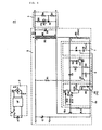
- the structure of a switching power supply unit according to a first embodiment of the present invention will be illustrated referring to Fig. 1.
- the switching power supply unit 1 shown in the figure is equivalent to the switching power supply unit 10 shown in Fig. 8, in which a delay circuit 6 and a rectifying and smoothing circuit 7 are added.
- the other parts except for these circuits 6 and 7 are given the same reference numerals as those in Fig. 8, and detailed explanation thereof is omitted.
- the delay circuit 6 constituting the switching power supply unit 1 includes a pnp-type transistor Q3 and a time-constant circuit composed of a capacitor C5 and a resistor R8.
- the emitter of the transistor Q3 is connected to one end of the feedback winding Nb of a transformer T via a capacitor C3 of a control circuit 5, whereas the collector thereof is connected to the gate of the FET Q1 via a resistor R13.
- the capacitor C5 constituting the delay circuit is connected between the base and the emitter of the transistor Q3.
- the rectifying and smoothing circuit 7 includes a rectifying diode D4 and a smoothing capacitor C6 mutually connected in series between both ends of the feedback winding Nb of the transformer T.
- the capacitor C6 of the rectifying and smoothing circuit 7 is charged by a voltage generated in the feedback winding Nb of the transformer T. Then, when energy charged in the transformer T is discharged on the secondary side and current flowing through the diode D1 on the secondary side is thereby zero, the charged voltage Vc1 of the capacitor C6 is discharged, and then, the capacitor C5 of the delay circuit 6 is charged by the charged voltage Vc1 and a voltage Vnb generated in the feedback winding Nb.
- the charged voltage Vc2 of the capacitor C5 reaches a voltage Von at which the transistor Q3 is turned on, and the transistor Q3 is thereby turned on, so that voltage is applied to the gate of the FET Q1 to turn on the FET Q1. That is, the turn-on of the FET Q1 is delayed until the charged voltage Vc2 reaches the voltage Von.
- the absolute value of the charged voltage Vc1 is increased in proportion to the load power of the switching power supply unit 1, as shown in Fig. 2, due to influence of leakage inductance of the transformer T or the like.
- the absolute value of the charged voltage Vc1 is relatively small, so that the time for the charging voltage Vc2 of the capacitor C5 the time-constant circuit to reach the voltage Von, at which the transistor Q3 is turned on, is longer. This permits the turn-on of the FET Q1 to be delayed so as to prolong the OFF time of the FET Q1, with the result that the switching frequency of the FET Q1 is reduced.
- the absolute value of the charged voltage Vc1 is relatively large, so that the time for the charging voltage Vc2 to reach the voltage Von, is shorter. This permits the turn-on of the FET Q1 to be accelerated so as to shorten the OFF time of the FET Q1.
- the drain current of the FET Q1 changes as shown in Fig. 3.
- This figure shows changes of the current waveform from light load to heavy load in the order of Figs. 3(a), 3(b), and 3(c).
- the symbol id indicates the waveform of the drain current of the FET Q1
- the symbol id1 indicates the waveform of the drain current of the main switching element used in a conventional switching power supply unit, which does not have a rectifying and smoothing circuit and a time-constant circuit.
- the symbol iD indicates the waveform of current flowing through the rectifying diode D1 on the secondary side of the transformer T
- the symbol iD1 indicates the waveform of current flowing through the rectifying diode on the secondary side of the conventional switching power supply unit having no rectifying and soothing circuits and no time-constant circuits.
- the main switching element used in the conventional switching power supply unit performs ON/OFF operations in reverse to ON/OFF operations of the rectifying diode, in which the symbols id1 and iD1 indicate mutually reversed waveforms.
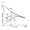
- Fig. 4(a) shows changes in the switching frequency with increase in a load power in the switching power supply unit 1. Regarding the value under light load, Fig. 4(a) is much lower than Fig. 4(d) showing the frequency of the conventional switching power supply unit having no rectifying and smoothing circuits and no time-constant circuits. The former frequency slowly rises with increase in the load to show the same change as that in the frequency (d) of the conventional switching power supply unit after a certain point.
- a Zener diode ZD is connected in series to a resistor R8 of a time-constant circuit of a delay circuit 6a.
- Fig. 4(b) shows changes in the switching frequency of the above switching power supply unit 1a.
- the value of the switching frequency is maintained lower than that of the frequency in the first embodiment shown in Fig. 4(a), until the sum of the charged voltage Vc1 of the capacitor C6 and the voltage Vnb occurring in a feedback winding Nb reaches the Zener voltage Vz of a Zener diode ZD.
- the Zener potential Vz of a Zener diode ZD.
- the switching frequency under heavy load abruptly rises, and the width of changes in the switching frequency is thereby increased.
- the switching frequency under light load is set to be significantly low in order to reduce switching losses, there is no problem of increase in conduction losses, since a switching frequency equivalent to that in the conventional switching power supply unit can be obtained under heavy load.
- a series circuit of a resistor R9 and a Zener diode ZD is connected in parallel to a resistor R8 of a time-constant circuit of a delay circuit 6b.
- Fig. 4(c) shows changes in the switching frequency of the switching power supply unit 1b having the above structure.
- a resistor R8 permits current flowing through transistor Q3 to be set very small, and the switching frequency thereby slowly rises.
- current abruptly flows into a resistor R9, and the time for the charging voltage Vc2 of a capacitor C5 to reach the voltage Von, at which the transistor Q3 is turned on, is shorter, with the result that the switching frequency abruptly rises.
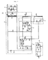
- FIG. 7 the structure of a switching power supply unit according to a fourth embodiment of the present invention will be illustrated below.
- an auxiliary feedback winding Nb1 in addition to a feedback winding Nb is disposed in a transformer T1, and a rectifying and smoothing circuit 7 is connected to the auxiliary feedback winding Nb1.
- the auxiliary feedback winding Nb1 is allowed to directly connect to the rectifying and smoothing circuit 7 not via a control circuit 5.
- the number of windings forming the auxiliary feedback winding Nb1 is not limited and can be greatly increased.
- the rectifying and smoothing circuit it is possible to connect the rectifying and smoothing circuit to a different auxiliary feedback winding from the feedback winding to which the control circuit is connected, so that the switching frequency under light load can be even further reduced in the respective switching power supply units.
- the capacitor of the time-constant circuit delaying the turn-on of the main switching element is charged by a voltage generated in the feedback winding of the transformer, as well as by the charged voltage of the capacitor of the rectifying and smoothing circuit connected to the feedback winding.
- the charged voltage of the capacitor of the rectifying and smoothing circuit increases in proportion to a load power due to the influence of a leakage inductance of the transformer, or the like.
- the absolute value of the charged voltage of the capacitor of the rectifying and smoothing circuit is relatively small, and the time for charging the capacitor of the time-constant circuit is thereby prolonged, so that the turn-on of the main switching element is delayed. Consequently, the OFF time of the main switching element is prolonged and the switching frequency is thereby lowered.
- the absolute value of the charged voltage of the capacitor of the rectifying and smoothing circuit is relatively large, and the turn-on of the main switching element is thereby accelerated, with the result that the OFF time of the main switching element is shortened.
- the switching frequency under heavy load can quickly be made a steep ascent by connecting a Zener diode in series to the resistor of the time-constant circuit, or connecting the rectifying and smoothing circuit to a different winding from the winding to which the control circuit is connected so as to increase the number of the windings. Accordingly, even if the switching frequency under light load is set to be significantly low in order to reduce switching losses, there is no problem of increase in continuity losses, since a switching frequency equivalent to that in the conventional switching power supply unit can be obtained under heavy load.
Landscapes
- Engineering & Computer Science (AREA)
- Power Engineering (AREA)
- Dc-Dc Converters (AREA)
Abstract
Description
Claims (8)
- A switching power supply unit comprising a DC power supply (2), a transformer (T) having a primary winding (N1), a secondary winding (N2) and a feedback winding (Nb), a main switching element (Q1) connected in series to the primary winding (N1), and a control circuit (5) connected between the feedback winding (Nb) and the control terminal of the main switching element (Q1) so that a DC output can be obtained, the main switching element (Q1) having an ON time, an OFF time and a switching frequency;
wherein there are provided a voltage generating circuit coupled to the transformer (T) to output a voltage in accordance with a load power and a delay circuit (6; 6a; 6b) for reducing the switching frequency by delaying turning on of the main switching element (Q1) according to a voltage output from the voltage generating circuit thereby prolonging the OFF time. - The switching power supply unit of Claim 1, wherein the voltage generating circuit comprises a rectifying and smoothing circuit (7) connected to the feedback winding (Nb).
- The switching power supply unit of Claim 1 or 2, wherein an auxiliary feedback winding (Nb1) connected between the control circuit (5) and the control terminal of the main switching element (Q1) is disposed in the transformer, and the voltage generating circuit comprises a rectifying and smoothing circuit (7) connected to the auxiliary feedback winding (Nb1).
- The switching power supply unit of one of Claims 1 to 3, wherein the delay circuit (6; 6a; 6b) comprises a switching device (Q3) disposed between the feedback winding (Nb) and a control terminal of the main switching element (Q1) and further comprises time-constant circuit (C5, R8) connected to the switching device (Q3).
- The switching power supply unit of Claim 4, wherein the time-constant circuit comprises a capacitor (C5) and a resistor (R8) connected to a control terminal of the switching device (Q3).
- The switching power supply unit of Claim 5, wherein a Zener diode (ZD) is connected in series to the resistor (R8) of the time-constant circuit.
- The switching power supply unit of Claim 5, further comprising a resistor (R9) connected in parallel to the resistor (R8) of the time-constant circuit and a Zener diode (ZD) is connected in series to one of the resistors (R8, R9).
- The switching power supply unit of claim 3, wherein the auxiliary feedback winding (Nb1) has a greater number of turns than the feedback winding (Nb) thereby to increase an output voltage of the auxiliary feedback winding (Nb1) to increase the voltage of the voltage generating circuit.
Applications Claiming Priority (4)
| Application Number | Priority Date | Filing Date | Title |
|---|---|---|---|
| JP946899 | 1999-01-18 | ||
| JP946899 | 1999-01-18 | ||
| JP25355099A JP3351400B2 (en) | 1999-01-18 | 1999-09-07 | Switching power supply |
| JP25355099 | 1999-09-07 |
Publications (3)
| Publication Number | Publication Date |
|---|---|
| EP1020980A2 true EP1020980A2 (en) | 2000-07-19 |
| EP1020980A3 EP1020980A3 (en) | 2001-11-14 |
| EP1020980B1 EP1020980B1 (en) | 2003-07-16 |
Family
ID=26344209
Family Applications (1)
| Application Number | Title | Priority Date | Filing Date |
|---|---|---|---|
| EP00100434A Expired - Lifetime EP1020980B1 (en) | 1999-01-18 | 2000-01-10 | Switching power supply unit |
Country Status (6)
| Country | Link |
|---|---|
| US (1) | US6295211B1 (en) |
| EP (1) | EP1020980B1 (en) |
| JP (1) | JP3351400B2 (en) |
| CN (1) | CN1174541C (en) |
| CA (1) | CA2296205C (en) |
| DE (1) | DE60003856D1 (en) |
Cited By (5)
| Publication number | Priority date | Publication date | Assignee | Title |
|---|---|---|---|---|
| EP1150417A1 (en) * | 2000-04-17 | 2001-10-31 | Murata Manufacturing Co., Ltd. | Switching power supply unit |
| GB2377096A (en) * | 2001-03-26 | 2002-12-31 | Murata Manufacturing Co | Switching power supply with feedback control |
| GB2393801A (en) * | 2002-08-20 | 2004-04-07 | Murata Manufacturing Co | Stabilised switching power supply circuit |
| EP1463191A3 (en) * | 2003-03-25 | 2005-10-19 | Orion Electric Company, Ltd. | Self-oscillating flyback converter |
| DE10143692B4 (en) * | 2000-09-06 | 2012-09-06 | Murata Mfg. Co., Ltd. | Switching power supply unit |
Families Citing this family (21)
| Publication number | Priority date | Publication date | Assignee | Title |
|---|---|---|---|---|
| JP3470693B2 (en) | 2000-10-25 | 2003-11-25 | 株式会社村田製作所 | Self-oscillation type switching power supply |
| TW583819B (en) * | 2000-12-19 | 2004-04-11 | Delta Electronics Inc | Apparatus and method of detecting circuit abnormality and protection for power converter |
| JP3760379B2 (en) * | 2000-12-28 | 2006-03-29 | 株式会社村田製作所 | Switching power supply |
| JP3548889B2 (en) | 2001-06-07 | 2004-07-28 | 株式会社村田製作所 | Switching power supply device and electronic device using the same |
| JP3712064B2 (en) * | 2002-05-08 | 2005-11-02 | セイコーエプソン株式会社 | Output overcurrent protection circuit and constant voltage switching power supply circuit having the output overcurrent protection circuit |
| US6661679B1 (en) | 2002-10-28 | 2003-12-09 | System General Corporation | PWM controller having adaptive off-time modulation for power saving |
| DE50301019D1 (en) * | 2003-07-15 | 2005-09-22 | Friwo Mobile Power Gmbh | Free-swinging flyback converter with current and voltage limitation |
| KR100693528B1 (en) * | 2004-10-29 | 2007-03-14 | 주식회사 팬택 | Wireless communication terminal with power delay authorization function |
| US7239119B2 (en) * | 2004-11-05 | 2007-07-03 | Power Integrations, Inc. | Method and apparatus to provide temporary peak power from a switching regulator |
| JP4446290B2 (en) * | 2006-03-02 | 2010-04-07 | 日立工機株式会社 | Electric tools and tabletop cutting machines |
| JP5042536B2 (en) * | 2006-06-16 | 2012-10-03 | ローム株式会社 | POWER SUPPLY DEVICE AND ELECTRIC DEVICE HAVING THE SAME |
| JP4910190B2 (en) * | 2006-08-10 | 2012-04-04 | 大平電子株式会社 | Soft switching circuit of self-excited switching power supply |
| CN100461603C (en) * | 2006-09-05 | 2009-02-11 | 广州金升阳科技有限公司 | Isolated self-oscillation reverse exciting inverter |
| KR101239978B1 (en) * | 2007-08-17 | 2013-03-06 | 삼성전자주식회사 | Switching mode power supply apparatus and power supply method thereof |
| JP5018960B2 (en) * | 2008-07-23 | 2012-09-05 | 株式会社村田製作所 | Isolated switching power supply |
| CN101453169B (en) * | 2008-12-02 | 2011-07-06 | 广州金升阳科技有限公司 | Self-oscillation starting output end controlled anti exciting converter |
| JP5683241B2 (en) * | 2010-12-06 | 2015-03-11 | キヤノン株式会社 | Switching power supply device and image forming apparatus |
| CN102291000B (en) * | 2011-08-29 | 2014-09-10 | 上海新进半导体制造有限公司 | Switch power supply integrated circuit |
| KR102233615B1 (en) | 2013-03-15 | 2021-03-30 | 다우 글로벌 테크놀로지스 엘엘씨 | Epdm packaging system and process |
| CN103683867B (en) * | 2013-12-06 | 2016-03-30 | 深圳市华星光电技术有限公司 | Inverse-excitation type switch power-supply circuit and apply the backlight driving device of this circuit |
| TWI756773B (en) * | 2020-08-05 | 2022-03-01 | 僑威科技股份有限公司 | Delay circuit and method for use in reducing relay switching |
Family Cites Families (14)
| Publication number | Priority date | Publication date | Assignee | Title |
|---|---|---|---|---|
| NL6705849A (en) * | 1967-04-26 | 1967-07-25 | ||
| JPS5531720B2 (en) * | 1972-12-04 | 1980-08-20 | ||
| NL8502339A (en) * | 1985-08-26 | 1987-03-16 | Philips Nv | SWITCHED POWER SUPPLY SWITCH WITH A POWER SWITCH. |
| US4862338A (en) * | 1986-09-29 | 1989-08-29 | Shindengen Kogyo Kabushiki Kaisha | Ringing choke converter using single switching element |
| JPH02159975A (en) * | 1988-12-09 | 1990-06-20 | Murata Mfg Co Ltd | Self-oscillation type converter |
| US5745353A (en) * | 1992-09-24 | 1998-04-28 | Kabushiki Kaisha Toshiba | Snubber circuit that suppresses surge and rush current flowing to a switching element of a self excitation-type flyback power supply |
| JP3028044B2 (en) * | 1995-04-17 | 2000-04-04 | 松下電器産業株式会社 | Switching power supply |
| JP3171068B2 (en) * | 1995-09-26 | 2001-05-28 | 株式会社村田製作所 | Switching power supply |
| JP3584606B2 (en) * | 1996-04-12 | 2004-11-04 | 株式会社ノーリツ | RCC switching system power supply circuit |
| JP3447471B2 (en) * | 1996-05-28 | 2003-09-16 | 新電元工業株式会社 | Switching power supply and surge voltage absorbing method using the switching power supply |
| JP3492882B2 (en) * | 1997-04-07 | 2004-02-03 | パイオニア株式会社 | Switching power supply |
| JP3175663B2 (en) * | 1997-10-17 | 2001-06-11 | 株式会社村田製作所 | Self-oscillation type switching power supply |
| JP3381769B2 (en) * | 1997-10-17 | 2003-03-04 | 株式会社村田製作所 | Self-oscillation type switching power supply |
| JP3216598B2 (en) * | 1998-02-09 | 2001-10-09 | 株式会社村田製作所 | Switching power supply |
-
1999
- 1999-09-07 JP JP25355099A patent/JP3351400B2/en not_active Expired - Fee Related
-
2000
- 2000-01-10 DE DE60003856T patent/DE60003856D1/en not_active Expired - Lifetime
- 2000-01-10 EP EP00100434A patent/EP1020980B1/en not_active Expired - Lifetime
- 2000-01-11 US US09/481,490 patent/US6295211B1/en not_active Expired - Fee Related
- 2000-01-17 CA CA002296205A patent/CA2296205C/en not_active Expired - Fee Related
- 2000-01-18 CN CNB001011162A patent/CN1174541C/en not_active Expired - Fee Related
Cited By (10)
| Publication number | Priority date | Publication date | Assignee | Title |
|---|---|---|---|---|
| EP1150417A1 (en) * | 2000-04-17 | 2001-10-31 | Murata Manufacturing Co., Ltd. | Switching power supply unit |
| US6532159B2 (en) | 2000-04-17 | 2003-03-11 | Murata Manufacturing Co., Ltd. | Switching power supply unit |
| DE10143692B4 (en) * | 2000-09-06 | 2012-09-06 | Murata Mfg. Co., Ltd. | Switching power supply unit |
| GB2377096A (en) * | 2001-03-26 | 2002-12-31 | Murata Manufacturing Co | Switching power supply with feedback control |
| GB2377096B (en) * | 2001-03-26 | 2003-05-07 | Murata Manufacturing Co | Switching power supply unit and electronic apparatus using the same |
| US6577511B2 (en) | 2001-03-26 | 2003-06-10 | Murata Manufacturing Co., Ltd. | Switching power supply unit and electronic apparatus using the same |
| GB2393801A (en) * | 2002-08-20 | 2004-04-07 | Murata Manufacturing Co | Stabilised switching power supply circuit |
| GB2393801B (en) * | 2002-08-20 | 2004-10-13 | Murata Manufacturing Co | Switching power supply unit and electronic apparatus using the same |
| US6898090B2 (en) | 2002-08-20 | 2005-05-24 | Murata Manufacturing Co., Ltd. | Switching power supply unit and electronic apparatus using the same |
| EP1463191A3 (en) * | 2003-03-25 | 2005-10-19 | Orion Electric Company, Ltd. | Self-oscillating flyback converter |
Also Published As
| Publication number | Publication date |
|---|---|
| CN1174541C (en) | 2004-11-03 |
| CA2296205C (en) | 2003-07-22 |
| DE60003856D1 (en) | 2003-08-21 |
| CA2296205A1 (en) | 2000-07-18 |
| JP2000278945A (en) | 2000-10-06 |
| CN1261221A (en) | 2000-07-26 |
| EP1020980B1 (en) | 2003-07-16 |
| JP3351400B2 (en) | 2002-11-25 |
| EP1020980A3 (en) | 2001-11-14 |
| US6295211B1 (en) | 2001-09-25 |
Similar Documents
| Publication | Publication Date | Title |
|---|---|---|
| EP1020980B1 (en) | Switching power supply unit | |
| US6788556B2 (en) | Switching power source device | |
| US6434029B1 (en) | Boost topology having an auxiliary winding on the snubber inductor | |
| US6529392B2 (en) | Switching power supply unit | |
| CN100517932C (en) | Switching power supply | |
| US6433443B2 (en) | Switching power supply having two or more DC outputs with switching circuit provided between the outputs | |
| US6233165B1 (en) | Power converter having a low voltage regulator powered from a high voltage source | |
| US6208530B1 (en) | Switching power supply device having main switching element period control circuit | |
| JP3760379B2 (en) | Switching power supply | |
| KR20250083520A (en) | Circuit for supplying power to the control circuit of a switching power supply based on auxiliary windings | |
| US4417153A (en) | High frequency switching circuit | |
| US6798671B1 (en) | Switching power supply unit | |
| KR100712749B1 (en) | DC / DC conversion circuit | |
| EP0935333A2 (en) | Switching power supply apparatus | |
| CN217134168U (en) | Transformer circuit and transformer system | |
| KR20000074998A (en) | Dc-dc converter | |
| JP3198831B2 (en) | Switching power supply | |
| KR100426605B1 (en) | Switching Power Supply Device Having Series Capacitance | |
| JPH08126313A (en) | Switching power supply | |
| JP3129037B2 (en) | Switching power supply | |
| JPH08280172A (en) | Dummy load circuit for switching power unit | |
| JPH073832Y2 (en) | Inrush current prevention circuit for switching power supply | |
| JPH06189545A (en) | Switching power supply | |
| JPH06113555A (en) | Discharge tube lighting circuit | |
| JPH05344721A (en) | Switching regulator |
Legal Events
| Date | Code | Title | Description |
|---|---|---|---|
| PUAI | Public reference made under article 153(3) epc to a published international application that has entered the european phase |
Free format text: ORIGINAL CODE: 0009012 |
|
| 17P | Request for examination filed |
Effective date: 20000110 |
|
| AK | Designated contracting states |
Kind code of ref document: A2 Designated state(s): AT BE CH CY DE DK ES FI FR GB GR IE IT LI LU MC NL PT SE Kind code of ref document: A2 Designated state(s): DE FR GB |
|
| AX | Request for extension of the european patent |
Free format text: AL;LT;LV;MK;RO;SI |
|
| PUAL | Search report despatched |
Free format text: ORIGINAL CODE: 0009013 |
|
| AK | Designated contracting states |
Kind code of ref document: A3 Designated state(s): AT BE CH CY DE DK ES FI FR GB GR IE IT LI LU MC NL PT SE |
|
| AX | Request for extension of the european patent |
Free format text: AL;LT;LV;MK;RO;SI |
|
| 17Q | First examination report despatched |
Effective date: 20020402 |
|
| AKX | Designation fees paid |
Free format text: DE FR GB |
|
| GRAH | Despatch of communication of intention to grant a patent |
Free format text: ORIGINAL CODE: EPIDOS IGRA |
|
| GRAH | Despatch of communication of intention to grant a patent |
Free format text: ORIGINAL CODE: EPIDOS IGRA |
|
| GRAA | (expected) grant |
Free format text: ORIGINAL CODE: 0009210 |
|
| AK | Designated contracting states |
Designated state(s): DE FR GB |
|
| PG25 | Lapsed in a contracting state [announced via postgrant information from national office to epo] |
Ref country code: FR Free format text: LAPSE BECAUSE OF FAILURE TO SUBMIT A TRANSLATION OF THE DESCRIPTION OR TO PAY THE FEE WITHIN THE PRESCRIBED TIME-LIMIT Effective date: 20030716 |
|
| REG | Reference to a national code |
Ref country code: GB Ref legal event code: FG4D |
|
| REF | Corresponds to: |
Ref document number: 60003856 Country of ref document: DE Date of ref document: 20030821 Kind code of ref document: P |
|
| PG25 | Lapsed in a contracting state [announced via postgrant information from national office to epo] |
Ref country code: DE Free format text: LAPSE BECAUSE OF FAILURE TO SUBMIT A TRANSLATION OF THE DESCRIPTION OR TO PAY THE FEE WITHIN THE PRESCRIBED TIME-LIMIT Effective date: 20031017 |
|
| PLBE | No opposition filed within time limit |
Free format text: ORIGINAL CODE: 0009261 |
|
| STAA | Information on the status of an ep patent application or granted ep patent |
Free format text: STATUS: NO OPPOSITION FILED WITHIN TIME LIMIT |
|
| 26N | No opposition filed |
Effective date: 20040419 |
|
| EN | Fr: translation not filed | ||
| PGFP | Annual fee paid to national office [announced via postgrant information from national office to epo] |
Ref country code: GB Payment date: 20110105 Year of fee payment: 12 |
|
| GBPC | Gb: european patent ceased through non-payment of renewal fee |
Effective date: 20120110 |
|
| PG25 | Lapsed in a contracting state [announced via postgrant information from national office to epo] |
Ref country code: GB Free format text: LAPSE BECAUSE OF NON-PAYMENT OF DUE FEES Effective date: 20120110 |