EP1020926A2 - Split gate memory cell - Google Patents
Split gate memory cell Download PDFInfo
- Publication number
- EP1020926A2 EP1020926A2 EP00300129A EP00300129A EP1020926A2 EP 1020926 A2 EP1020926 A2 EP 1020926A2 EP 00300129 A EP00300129 A EP 00300129A EP 00300129 A EP00300129 A EP 00300129A EP 1020926 A2 EP1020926 A2 EP 1020926A2
- Authority
- EP
- European Patent Office
- Prior art keywords
- gate
- control gate
- memory cell
- voltage
- substrate
- Prior art date
- Legal status (The legal status is an assumption and is not a legal conclusion. Google has not performed a legal analysis and makes no representation as to the accuracy of the status listed.)
- Withdrawn
Links
Images


Classifications
-
- H—ELECTRICITY
- H10—SEMICONDUCTOR DEVICES; ELECTRIC SOLID-STATE DEVICES NOT OTHERWISE PROVIDED FOR
- H10B—ELECTRONIC MEMORY DEVICES
- H10B69/00—Erasable-and-programmable ROM [EPROM] devices not provided for in groups H10B41/00 - H10B63/00, e.g. ultraviolet erasable-and-programmable ROM [UVEPROM] devices
-
- H—ELECTRICITY
- H10—SEMICONDUCTOR DEVICES; ELECTRIC SOLID-STATE DEVICES NOT OTHERWISE PROVIDED FOR
- H10D—INORGANIC ELECTRIC SEMICONDUCTOR DEVICES
- H10D30/00—Field-effect transistors [FET]
- H10D30/60—Insulated-gate field-effect transistors [IGFET]
- H10D30/68—Floating-gate IGFETs
- H10D30/681—Floating-gate IGFETs having only two programming levels
- H10D30/684—Floating-gate IGFETs having only two programming levels programmed by hot carrier injection
- H10D30/685—Floating-gate IGFETs having only two programming levels programmed by hot carrier injection from the channel
-
- H—ELECTRICITY
- H10—SEMICONDUCTOR DEVICES; ELECTRIC SOLID-STATE DEVICES NOT OTHERWISE PROVIDED FOR
- H10D—INORGANIC ELECTRIC SEMICONDUCTOR DEVICES
- H10D30/00—Field-effect transistors [FET]
- H10D30/01—Manufacture or treatment
- H10D30/021—Manufacture or treatment of FETs having insulated gates [IGFET]
- H10D30/0411—Manufacture or treatment of FETs having insulated gates [IGFET] of FETs having floating gates
-
- H—ELECTRICITY
- H10—SEMICONDUCTOR DEVICES; ELECTRIC SOLID-STATE DEVICES NOT OTHERWISE PROVIDED FOR
- H10D—INORGANIC ELECTRIC SEMICONDUCTOR DEVICES
- H10D30/00—Field-effect transistors [FET]
- H10D30/60—Insulated-gate field-effect transistors [IGFET]
- H10D30/68—Floating-gate IGFETs
- H10D30/6891—Floating-gate IGFETs characterised by the shapes, relative sizes or dispositions of the floating gate electrode
- H10D30/6892—Floating-gate IGFETs characterised by the shapes, relative sizes or dispositions of the floating gate electrode having at least one additional gate other than the floating gate and the control gate, e.g. program gate, erase gate or select gate
-
- H—ELECTRICITY
- H10—SEMICONDUCTOR DEVICES; ELECTRIC SOLID-STATE DEVICES NOT OTHERWISE PROVIDED FOR
- H10D—INORGANIC ELECTRIC SEMICONDUCTOR DEVICES
- H10D64/00—Electrodes of devices having potential barriers
- H10D64/01—Manufacture or treatment
- H10D64/031—Manufacture or treatment of data-storage electrodes
- H10D64/035—Manufacture or treatment of data-storage electrodes comprising conductor-insulator-conductor-insulator-semiconductor structures
Definitions
- the present invention relates to a memory cell and more particularly a split gate memory cell useful for low voltage operation.
- the present invention comprises a novel split gate memory cell and its method of operation.
- the novel split gate cell comprises a silicon substrate having a tunnel oxide layer on a portion of its surface and a first control gate and a floating gate electrode spaced from each other and preferably formed from the same material over the tunnel oxide.
- a dielectric layer overlies the first control gate and the floating gate electrodes, including the surface of the electrodes in the area between them.
- a second control gate, which is physically separated from the first control gate is provide over the dielectric layer and in the space between the first control gate and the floating gate.
- a highly doped region may be provided in the silicon substrate in the region under the separation of the first control gate and the floating gate. Source and drain regions are also provided in the substrate with optional halo-implants adjacent thereto.
- the novel memory cell is fabricated by providing a tunnel oxide layer on the surface of a silicon substrate; forming a conductive layer over the tunnel oxide; forming a space in the conductive layer so as to provide a control gate and a floating gate electrode separated from each other but made from the same deposited or grown layer; forming a highly doped region in the substrate below the space between the aforementioned electrodes; forming a dielectric layer over the surfaces of the aforementioned electrodes; and forming a second control gate over the dielectric layer.
- the novel device can operate at lower voltages than conventional split gate memory cells.
- the device is programmed by first applying a voltage to the second control gate, electrically floating the node second control gate and the applying a voltage to the first control gate. Due to a coupling between control gates, the voltage on the second control gate is automatically increased upon application of a voltage to the first control gate. The drain may then be pulsed to initiate hot carrier injection into the floating gate or a small charge pump may be provided to generate higher voltages.
- erasure can be accomplished with the first control gate open and and the second control gate held at a negative voltage with a positive drain voltage. Alternatively, one can erase utilizing a low voltage charge pump from the coupling between the control gates but using a negative voltage. Further, erase can be accomplished by a channel erase process. During the Read operation, both of the control gates are brought to the wordline voltage.
- FG is a storage node made of floating gate polysilicon or other conductor
- CG-1 is a control gate also made from polysilicon or other appropriate conductor
- CG-2 is a control gate made of polysilicon, which may be silicided, or other conductor.
- the FG and CG-1 layers are sometimes referred to as poly-1 since they are formed from the same deposited or grown layer (poly-1).
- the CG-2 gate is sometimes referred to as poly-2 as it is formed from a deposited layer designated as poly-2.
- Polysilicon is preferred over other conductors for both the poly-1 and poly-2 layers.
- the process for making the novel device 10 includes the growth of a tunnel oxide 12 on a silicon substrate 14 after conventional IC isolation and active area definition steps have been finished.
- the thickness of the tunnel oxide is from 50-150A and preferably between about 80-100A.
- An in-situ doped polysilicon layer, poly-1, (or other conductor) 16 is then deposited.
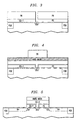
- the poly-1 is then patterned by means of a thick gate photoresist (PR-1), as shown in Fig 3A and the device is etched to form the individual, separated FG and CG-1 structures as shown in Fig. 3B.
- PR-1 thick gate photoresist
- An optional N + ion implant 18 in the silicon wafer substrate 14 in the region of the separation between CG-1 and FG is preferably performed.
- the resist, PR-1, used for implantation is removed, the tunnel oxide etched, and an interpoly dielectric layer 20 is deposited on the wafers to isolate the poly-1 CG-1 and FG structures from the subsequently deposited poly-2 layer 22.
- the interpoly dielectric layer 20 can be made of silicon dioxide, an ONO (oxide/nitride/oxide) composite or a known high K dielectric to achieve the necessary coupling.
- the interpoly layer 20 is from 50-300A thick and and generally about 180A thick for a silicon oxide layer.
- the thickness of the interpoly layer 20 depends upon the material employed for that layer.
- the dielectric may be removed from selected areas where a gate-dielectric thinner than the high voltage dielectric may be needed, e.g. for embedded applications, analogous to the thick gate operation.
- a disposable hard mask 24 is deposited over the poly-2 layer 22.
- a gate photoresist, PR-2 is then deposited over the hard mask 24 so as to define the width of the split gate cell and the device is etched, stopping after the poly-2 layer 22.
- the core CMOS area is protected with a photoresist (not shown), and the memory cell area is opened for a gate stack etch.
- a source/drain halo ion implant 26 is then implanted, followed by a heavy dose source/drain arsenic ion implant 28 resulting in the structure shown in Fig. 5B.
- Boron, boron fluoride or any other P-type dopant, implanted preferably with a large tilt angle can be used for the drain halo implant 26.
- asymmetric device with, for example, a halo implant in the drain end only.
- Such asymmetric device generally exhibits a higher read current and has a higher speed as compared with the symmetrical device depicted in the Figures.
- CMOS processing is completed, and the hard-mask 24 is removed as part of the core CMOS process to arrive at the novel device represented by Fig. 2.
- the device With contacts open to drain, source, CG-1 and CG-2, the device may be used as a NVRAM for low voltage operation. Also, it may be noted that the process sequence allows one to use thicker oxides, formed by the composite of deposited HTO and grown oxide, for use in high voltage devices.
- a preferred process for making a small space between FG and CG-1 is shown with reference to Figs. 6-8.
- the process comprises growing the tunnel oxide 12, depositing the poly-1 layer 16, depositing a thin undoped silicon oxide dopant mask layer 30 followed by the deposition of a disposable doped oxide layer 32, e.g. a boron-phosphorous silicate glass (BPTEOS).
- BPTEOS boron-phosphorous silicate glass
- a patterned photoresist layer 34 is provided and the device is etched removing the exposed portion of the doped oxide layer 32 and undoped oxide mask layer 30 stopping at poly-1. This results in the structure shown in Fig. 6.
- the photoresist 34 is then removed, the surface is cleaned and a disposable oxide dopant mask 36 is grown/deposited.
- a BPTEOS spacer oxide 38 is deposited and a timed spacer etch is performed to reach the structure of Fig. 7. Finally, the poly-1 layer 16 is etched to form the separated CG-1 and FG areas. As previously indicated and as shown in Fig. 8, a N-type dopant (e.g. AS) is implanted in the space between the CG-1 and FG areas. Thereafter, the disposable oxide is etched away in an ammonium hydroxide/hydrogen peroxide bath. Device formation may then proceed essentially as described above with reference to Figs. 4A, 4B ,5A and 5B.
- a N-type dopant e.g. AS
- the control gates, CG-1 and CG-2 are made of the same polysilicon and are physically connected. Also, the thickness of the tunneling oxides under the FG and CG gates are generally different, making fabrication more complex.
- a large voltage ( ⁇ 7.5V) on the control gate to achieve programming in a short time ( ⁇ a few 10's of ⁇ s). This however does not allow one to scale the underlying select-gate oxide.
- the voltage on CG-1 can be limited to ⁇ 5V so that one can use the tunnel oxide as the gate of the select-gate oxide.
- the coupling ratio between the CG-2 and the CG-1 can be high, e.g. ⁇ 0.6, which is approximately similar to the coupling between CG-2 and FG.
- CG-2 e.g. ⁇ 5.0V
- the node CG-2 is electrically floated and the voltage on CG-1 is brought up, e.g. to ⁇ 5V.
- the coupling between CG-1 and CG-2 is about 0.6 so the voltage on CG-2 is increased to ⁇ 8V.
- the drain may be pulsed to initiate hot carrier generation and injection into the FG.
- Another advantage of using the structure of this invention is that the vertical field in the injection region can be independent of the select-gate voltage. Thus, if one chooses, one can apply a large voltage to CG-2 to increase the vertical field and at the same time apply a small voltage to CG-1 to limit programming current and thus improve injection efficiency, as is done in source side injection cells. Such a programming scheme allows one to conserve power in low power applications.
- ERASURE In a conventional split gate device, during erase a large negative voltage is applied to CG-2 and the drain is held at a large positive voltage. Such a scheme is also possible in the structure of the present invention. With CG-1 open and CG-2 at a negative voltage a positive drain voltage can duplicate the erase of a conventional split gate cell. However, the present cell offers the option of using a lower voltage charge pump and using the built-in charge pump for erase, in a manner analogous to programming but with negative voltages.
- channel erase is difficult to achieve due to the large coupling ratio between the substrate and FG. Due to this coupling one needs very large substrate voltages, e.g. >15V, to initiate tunneling from the floating gate to the substrate. This voltage appears across the select gate oxide and in order to prevent dielectric breakdown, thicker oxides than those required in the device of the present invention would be required. However, such thicker oxides degrade device performance. In contrast, one can readily utilize a channel erase in the present invention. Here, even if 15 volts is applied to the substrate, one can hold CG1 at 7.5V, with CG2 at 0V and thus the fields across the oxides in the select gate region is ⁇ 7.5V in all cases.
- substrate voltages e.g. >15V
- READ Read of the devices can follow in a normal fashion with the exception that during read, both CG-1 and CG-2 are brought up to the wordline voltage.
- the effective capacitance of the wordline is thus similar in value to what it would be for a conventional split gate device (with a thinner gate oxide). With a thinner select-gate oxide (cf. to a conventional split gate cell), a higher on-current and thus a higher read speed is to be expected.
Landscapes
- Non-Volatile Memory (AREA)
- Semiconductor Memories (AREA)
Abstract
Description
Claims (23)
- A semiconductor device comprising a p-type silicon substrate having a tunnel oxide on its surface, an n+-type source and an n+-type drain separated from each other and implanted in said substrate, and on said substrate between said source and drain and over said tunnel oxide, a floating gate polysilicon storage node and a first polysilicon control gate separated from the floating gate storage node on said tunnel oxide, a second polysilicon control gate between and over the polysilicon control gate and the floating gate and isolated therefrom by a dielectric layer.
- The semiconductor device recited in claim 1 further including a n+-type implant in the substrate in the region under the separation between the floating gate and the first control gate.
- A split gate memory cell comprising a silicon substrate, a tunnel oxide layer on said substrate, a first control gate and a floating gate over said tunnel oxide, said first control gate and said floating gate being separated from each other by a space, a dielectric layer over the surfaces of said first control gate and floating gate, a second control gate over the dielectric layer and extending within said space, and separated source and drain regions in said substrate adjacent the first control gate and floating gate.
- The split gate memory cell recited in claim 3 further including a highly doped region in said substrate under said space, of opposite conductivity type from the substrate.
- The split gate memory cell recited in claim 3 wherein said space is in the order of 0.1 microns.
- The split gate memory cell recited in claim 3 wherein the first control gate and floating gate are formed from the same conductive layer.
- The split gate memory cell recited in claim 6 wherein said first control gate and floating gate comprise polysilicon.
- The split gate memory cell recited in claim 7 wherein said second control gate comprises a member of the group consisting of polysilicon and a silicided polysilicon.
- The split gate memory cell recited in claim 8 wherein said dielectric layer comprises at least one member of the group consisting of silicon dioxide, an oxide/nitride/oxide composite and a high k dielectric material.
- A split gate memory cell comprises a silicon substrate having a silicon dioxide tunnel layer thereon, a first control gate electrode and a floating gate electrode spaced from said first control gate electrode overlying said tunnel layer and comprised of polysilicon, a dielectric layer over the surface of said first control gate and said floating gate electrodes, and a second control gate electrode comprised of a polysilicon over said dielectric layer on both the first control gate and floating gate electrodes and in said space between said electrodes.
- The split gate memory cell recited in claim 10 further comprising an n+ doped region in the substrate under said space.
- A split gate memory cell comprising a first and a second control gate and a floating gate, said gates isolated one from the other by a dielectric layer and said first control gate and said floating gate being on the same plane and having a space therebetween and overlying a tunnel oxide layer.
- The split gate memory cell recited in claim 12 wherein said substrate has a highly doped region under said space.
- A method of programming a split gate memory cell of the type set forth in claim 3 comprising applying a voltage of a first polarity across the second control gate, electrically floating said floating gate, applying a voltage of the first polarity to the first control gate to cause the voltage on the second control gate to increase due to coupling between said control gates, and initiating hot carrier generation and injection into said floating gate.
- The method recited in claim 14 wherein the magnitude of the voltages applied to the first and second control gates are approximately the same.
- The method recited in claim 14 wherein the voltage applied to the second control gate is greater than the voltage applied to the first control gate.
- A method of erasing data stored in a split gate memory cell of the type claimed claim 3 comprising applying a drain voltage of a first polarity and a voltage of opposite polarity to the second control gate while the first control gate is open.
- The method of erasing data stored in a split gate memory cell of the type set forth claim 3 comprising the steps set forth in claim 14 for programming, but applying voltages to the control gates of opposite polarity from that used for programming.
- A method of reading data stored in a split gate memory cell of the type recited claim 3 including the step of bringing the voltage of both the first and second control gates to wordline voltage.
- The device recited in claim 4 wherein the source and drain regions are n+-type regions and further including at least one p+-type halo-implant region in the substrate adjacent at least one of said regions.
- The device recited in claim 20 further including a halo implant adjacent both the source and drain regions.
- The device recited in claim 20 wherein there is a halo-implant adjacent the drain region, but not the source region of the device.
- A channel erase method for erasing data stored in a split-gate memory cell of the type set forth in claim 3 comprising applying a first voltage to the substrate, holding the voltage to the first control gate at about half of the voltage applied to the substrate and the voltage of the second control gate at or about zero volts such that the fields across the oxides in the select gate region are less than 7.5 mv/cm.
Applications Claiming Priority (4)
| Application Number | Priority Date | Filing Date | Title |
|---|---|---|---|
| US11560299P | 1999-01-12 | 1999-01-12 | |
| US115602P | 1999-01-12 | ||
| US460812 | 1999-12-14 | ||
| US09/460,812 US6313500B1 (en) | 1999-01-12 | 1999-12-14 | Split gate memory cell |
Publications (2)
| Publication Number | Publication Date |
|---|---|
| EP1020926A2 true EP1020926A2 (en) | 2000-07-19 |
| EP1020926A3 EP1020926A3 (en) | 2002-01-16 |
Family
ID=26813373
Family Applications (1)
| Application Number | Title | Priority Date | Filing Date |
|---|---|---|---|
| EP00300129A Withdrawn EP1020926A3 (en) | 1999-01-12 | 2000-01-11 | Split gate memory cell |
Country Status (5)
| Country | Link |
|---|---|
| US (1) | US6313500B1 (en) |
| EP (1) | EP1020926A3 (en) |
| JP (1) | JP2000208651A (en) |
| KR (1) | KR20000057745A (en) |
| SG (2) | SG84558A1 (en) |
Cited By (3)
| Publication number | Priority date | Publication date | Assignee | Title |
|---|---|---|---|---|
| FR2852735A1 (en) * | 2003-03-17 | 2004-09-24 | Samsung Electronics Co Ltd | LOCAL SONOS STRUCTURE FOR NON-VOLATILE SEMICONDUCTOR MEMORY AND METHOD OF MANUFACTURING |
| CN110061057A (en) * | 2019-05-06 | 2019-07-26 | 重庆大学 | A kind of superjunction power MOSFET with integrated tunnel-through diode |
| WO2022226947A1 (en) * | 2021-04-29 | 2022-11-03 | 华为技术有限公司 | Memory having tfet |
Families Citing this family (11)
| Publication number | Priority date | Publication date | Assignee | Title |
|---|---|---|---|---|
| DE10138585A1 (en) * | 2001-08-06 | 2003-03-06 | Infineon Technologies Ag | memory cell |
| US7064034B2 (en) | 2002-07-02 | 2006-06-20 | Sandisk Corporation | Technique for fabricating logic elements using multiple gate layers |
| KR100848248B1 (en) * | 2002-12-28 | 2008-07-24 | 동부일렉트로닉스 주식회사 | Flash memory device and manufacturing method thereof |
| US20040197992A1 (en) * | 2003-04-03 | 2004-10-07 | Hsiao-Ying Yang | Floating gates having improved coupling ratios and fabrication method thereof |
| US7091566B2 (en) * | 2003-11-20 | 2006-08-15 | International Business Machines Corp. | Dual gate FinFet |
| US7075127B2 (en) * | 2004-01-29 | 2006-07-11 | Infineon Technologies Ag | Single-poly 2-transistor based fuse element |
| US7335941B2 (en) * | 2004-07-14 | 2008-02-26 | Taiwan Semiconductor Manufacturing Company, Ltd. | Uniform channel programmable erasable flash EEPROM |
| US7622349B2 (en) * | 2005-12-14 | 2009-11-24 | Freescale Semiconductor, Inc. | Floating gate non-volatile memory and method thereof |
| US8320191B2 (en) | 2007-08-30 | 2012-11-27 | Infineon Technologies Ag | Memory cell arrangement, method for controlling a memory cell, memory array and electronic device |
| US9397176B2 (en) * | 2014-07-30 | 2016-07-19 | Freescale Semiconductor, Inc. | Method of forming split gate memory with improved reliability |
| US11848378B2 (en) | 2020-08-13 | 2023-12-19 | Stmicroelectronics Pte Ltd | Split-gate trench power MOSFET with self-aligned poly-to-poly isolation |
Family Cites Families (15)
| Publication number | Priority date | Publication date | Assignee | Title |
|---|---|---|---|---|
| JPS63245959A (en) * | 1987-04-01 | 1988-10-13 | Nec Corp | Nonvolatile memory cell |
| JPH07120719B2 (en) * | 1987-12-02 | 1995-12-20 | 三菱電機株式会社 | Semiconductor memory device |
| US5278439A (en) * | 1991-08-29 | 1994-01-11 | Ma Yueh Y | Self-aligned dual-bit split gate (DSG) flash EEPROM cell |
| US5273923A (en) * | 1991-10-09 | 1993-12-28 | Motorola, Inc. | Process for fabricating an EEPROM cell having a tunnel opening which overlaps field isolation regions |
| JP2975824B2 (en) * | 1993-11-18 | 1999-11-10 | 三洋電機株式会社 | Nonvolatile semiconductor memory device |
| US5422504A (en) * | 1994-05-02 | 1995-06-06 | Motorola Inc. | EEPROM memory device having a sidewall spacer floating gate electrode and process |
| US5440158A (en) * | 1994-07-05 | 1995-08-08 | Taiwan Semiconductor Manufacturing Company Ltd. | Electrically programmable memory device with improved dual floating gates |
| US5439838A (en) * | 1994-09-14 | 1995-08-08 | United Microelectronics Corporation | Method of thinning for EEPROM tunneling oxide device |
| US5714412A (en) * | 1996-12-02 | 1998-02-03 | Taiwan Semiconductor Manufacturing Company, Ltd | Multi-level, split-gate, flash memory cell and method of manufacture thereof |
| US5867425A (en) * | 1997-04-11 | 1999-02-02 | Wong; Ting-Wah | Nonvolatile memory capable of using substrate hot electron injection |
| US6093945A (en) * | 1998-07-09 | 2000-07-25 | Windbond Electronics Corp. | Split gate flash memory with minimum over-erase problem |
| IT1301880B1 (en) * | 1998-07-30 | 2000-07-07 | St Microelectronics Srl | ELECTRONIC MEMORY CIRCUIT AND CORRESPONDING MANUFACTURING METHOD |
| KR100297603B1 (en) * | 1998-08-13 | 2001-08-07 | 윤종용 | Flash type nonvolatile semiconductor memory device for preventing over erasure |
| US6103573A (en) * | 1999-06-30 | 2000-08-15 | Sandisk Corporation | Processing techniques for making a dual floating gate EEPROM cell array |
| US6087695A (en) * | 1999-08-20 | 2000-07-11 | Worldwide Semiconductor Mfg | Source side injection flash EEPROM memory cell with dielectric pillar and operation |
-
1999
- 1999-12-14 US US09/460,812 patent/US6313500B1/en not_active Expired - Lifetime
-
2000
- 2000-01-11 SG SG200000120A patent/SG84558A1/en unknown
- 2000-01-11 SG SG200000123A patent/SG82667A1/en unknown
- 2000-01-11 EP EP00300129A patent/EP1020926A3/en not_active Withdrawn
- 2000-01-12 JP JP3633A patent/JP2000208651A/en active Pending
- 2000-01-12 KR KR1020000001298A patent/KR20000057745A/en not_active Withdrawn
Cited By (5)
| Publication number | Priority date | Publication date | Assignee | Title |
|---|---|---|---|---|
| FR2852735A1 (en) * | 2003-03-17 | 2004-09-24 | Samsung Electronics Co Ltd | LOCAL SONOS STRUCTURE FOR NON-VOLATILE SEMICONDUCTOR MEMORY AND METHOD OF MANUFACTURING |
| CN110061057A (en) * | 2019-05-06 | 2019-07-26 | 重庆大学 | A kind of superjunction power MOSFET with integrated tunnel-through diode |
| CN110061057B (en) * | 2019-05-06 | 2020-08-18 | 重庆大学 | Super junction power MOSFET with integrated tunneling diode |
| WO2022226947A1 (en) * | 2021-04-29 | 2022-11-03 | 华为技术有限公司 | Memory having tfet |
| CN116649004A (en) * | 2021-04-29 | 2023-08-25 | 华为技术有限公司 | A kind of memory with TFET |
Also Published As
| Publication number | Publication date |
|---|---|
| KR20000057745A (en) | 2000-09-25 |
| JP2000208651A (en) | 2000-07-28 |
| US6313500B1 (en) | 2001-11-06 |
| EP1020926A3 (en) | 2002-01-16 |
| SG82667A1 (en) | 2001-08-21 |
| SG84558A1 (en) | 2001-11-20 |
Similar Documents
| Publication | Publication Date | Title |
|---|---|---|
| US6885586B2 (en) | Self-aligned split-gate NAND flash memory and fabrication process | |
| US6958513B2 (en) | Floating-gate memory cell having trench structure with ballistic-charge injector, and the array of memory cells | |
| KR100274491B1 (en) | Spacer Flash Cell Process | |
| US5824584A (en) | Method of making and accessing split gate memory device | |
| US7307308B2 (en) | Buried bit line non-volatile floating gate memory cell with independent controllable control gate in a trench, and array thereof, and method of formation | |
| US6764905B2 (en) | Method of manufacturing a scalable flash EEPROM memory cell with floating gate spacer wrapped by control gate | |
| US6458656B1 (en) | Process for creating a flash memory cell using a photoresist flow operation | |
| US20160372561A1 (en) | Memory cell having a vertical selection gate formed in an fdsoi substrate | |
| US20040256661A1 (en) | Nonvolatile memory capable of storing multibits binary information and the method of forming the same | |
| US6168995B1 (en) | Method of fabricating a split gate memory cell | |
| EP1687826A2 (en) | Flash memory programming using gate induced junction leakage current | |
| KR102767451B1 (en) | Separate gate nonvolatile memory cell having an erase gate arranged over a word line gate, and method for manufacturing the same | |
| US6313500B1 (en) | Split gate memory cell | |
| US20210036117A1 (en) | Memory And Method For Forming The Same | |
| US5023694A (en) | Side wall contact in a nonvolatile electrically alterable memory cell | |
| US7145802B2 (en) | Programming and manufacturing method for split gate memory cell | |
| US6362052B1 (en) | Use of an etch to reduce the thickness and around the edges of a resist mask during the creation of a memory cell | |
| US5057446A (en) | Method of making an EEPROM with improved capacitive coupling between control gate and floating gate | |
| EP0612108B1 (en) | Double polysilicon EEPROM cell and corresponding manufacturing process | |
| US6486029B1 (en) | Integration of an ion implant hard mask structure into a process for fabricating high density memory cells | |
| US6878986B2 (en) | Embedded flash memory cell having improved programming and erasing efficiency | |
| US6596587B1 (en) | Shallow junction EEPROM device and process for fabricating the device | |
| US6846714B1 (en) | Voltage limited EEPROM device and process for fabricating the device | |
| KR20000057746A (en) | Method of fabricating a split gate memory cell | |
| KR100383083B1 (en) | Flash memory having low operation voltage and manufacturing method thereof |
Legal Events
| Date | Code | Title | Description |
|---|---|---|---|
| PUAI | Public reference made under article 153(3) epc to a published international application that has entered the european phase |
Free format text: ORIGINAL CODE: 0009012 |
|
| AK | Designated contracting states |
Kind code of ref document: A2 Designated state(s): AT BE CH CY DE DK ES FI FR GB GR IE IT LI LU MC NL PT SE |
|
| AX | Request for extension of the european patent |
Free format text: AL;LT;LV;MK;RO;SI |
|
| PUAL | Search report despatched |
Free format text: ORIGINAL CODE: 0009013 |
|
| AK | Designated contracting states |
Kind code of ref document: A3 Designated state(s): AT BE CH CY DE DK ES FI FR GB GR IE IT LI LU MC NL PT SE |
|
| AX | Request for extension of the european patent |
Free format text: AL;LT;LV;MK;RO;SI |
|
| AKX | Designation fees paid | ||
| REG | Reference to a national code |
Ref country code: DE Ref legal event code: 8566 |
|
| STAA | Information on the status of an ep patent application or granted ep patent |
Free format text: STATUS: THE APPLICATION IS DEEMED TO BE WITHDRAWN |
|
| 18D | Application deemed to be withdrawn |
Effective date: 20020717 |