EP1020902A2 - Method of fabricating a split gate memory cell - Google Patents
Method of fabricating a split gate memory cell Download PDFInfo
- Publication number
- EP1020902A2 EP1020902A2 EP00300131A EP00300131A EP1020902A2 EP 1020902 A2 EP1020902 A2 EP 1020902A2 EP 00300131 A EP00300131 A EP 00300131A EP 00300131 A EP00300131 A EP 00300131A EP 1020902 A2 EP1020902 A2 EP 1020902A2
- Authority
- EP
- European Patent Office
- Prior art keywords
- layer
- forming
- conductive layer
- over
- gate electrode
- Prior art date
- Legal status (The legal status is an assumption and is not a legal conclusion. Google has not performed a legal analysis and makes no representation as to the accuracy of the status listed.)
- Withdrawn
Links
- 238000004519 manufacturing process Methods 0.000 title claims abstract description 6
- 239000000758 substrate Substances 0.000 claims abstract description 16
- 238000007667 floating Methods 0.000 claims abstract description 14
- 238000000151 deposition Methods 0.000 claims abstract description 8
- XUIMIQQOPSSXEZ-UHFFFAOYSA-N Silicon Chemical compound [Si] XUIMIQQOPSSXEZ-UHFFFAOYSA-N 0.000 claims abstract description 7
- 229910052710 silicon Inorganic materials 0.000 claims abstract description 7
- 239000010703 silicon Substances 0.000 claims abstract description 7
- 238000005530 etching Methods 0.000 claims abstract 4
- VYPSYNLAJGMNEJ-UHFFFAOYSA-N Silicium dioxide Chemical compound O=[Si]=O VYPSYNLAJGMNEJ-UHFFFAOYSA-N 0.000 claims description 16
- 238000000034 method Methods 0.000 claims description 16
- 229920002120 photoresistant polymer Polymers 0.000 claims description 12
- 239000007943 implant Substances 0.000 claims description 10
- 229910021420 polycrystalline silicon Inorganic materials 0.000 claims description 10
- 229920005591 polysilicon Polymers 0.000 claims description 10
- 239000000377 silicon dioxide Substances 0.000 claims description 6
- 235000012239 silicon dioxide Nutrition 0.000 claims description 6
- 239000002019 doping agent Substances 0.000 claims description 5
- 125000006850 spacer group Chemical group 0.000 claims description 5
- 150000002500 ions Chemical class 0.000 claims description 4
- 229910052814 silicon oxide Inorganic materials 0.000 claims description 4
- 230000008878 coupling Effects 0.000 description 6
- 238000010168 coupling process Methods 0.000 description 6
- 238000005859 coupling reaction Methods 0.000 description 6
- 239000004020 conductor Substances 0.000 description 5
- 238000002347 injection Methods 0.000 description 4
- 239000007924 injection Substances 0.000 description 4
- 230000015556 catabolic process Effects 0.000 description 3
- 125000001475 halogen functional group Chemical group 0.000 description 3
- MHAJPDPJQMAIIY-UHFFFAOYSA-N Hydrogen peroxide Chemical compound OO MHAJPDPJQMAIIY-UHFFFAOYSA-N 0.000 description 2
- 230000008901 benefit Effects 0.000 description 2
- 239000002131 composite material Substances 0.000 description 2
- 239000000463 material Substances 0.000 description 2
- 238000000926 separation method Methods 0.000 description 2
- 238000003860 storage Methods 0.000 description 2
- 230000005641 tunneling Effects 0.000 description 2
- 235000012431 wafers Nutrition 0.000 description 2
- VHUUQVKOLVNVRT-UHFFFAOYSA-N Ammonium hydroxide Chemical compound [NH4+].[OH-] VHUUQVKOLVNVRT-UHFFFAOYSA-N 0.000 description 1
- 229910015900 BF3 Inorganic materials 0.000 description 1
- ZOXJGFHDIHLPTG-UHFFFAOYSA-N Boron Chemical compound [B] ZOXJGFHDIHLPTG-UHFFFAOYSA-N 0.000 description 1
- 239000000908 ammonium hydroxide Substances 0.000 description 1
- HAYXDMNJJFVXCI-UHFFFAOYSA-N arsenic(5+) Chemical compound [As+5] HAYXDMNJJFVXCI-UHFFFAOYSA-N 0.000 description 1
- 230000015572 biosynthetic process Effects 0.000 description 1
- 229910052796 boron Inorganic materials 0.000 description 1
- WTEOIRVLGSZEPR-UHFFFAOYSA-N boron trifluoride Chemical compound FB(F)F WTEOIRVLGSZEPR-UHFFFAOYSA-N 0.000 description 1
- 230000008021 deposition Effects 0.000 description 1
- 238000011982 device technology Methods 0.000 description 1
- -1 halo ion Chemical class 0.000 description 1
- 238000002513 implantation Methods 0.000 description 1
- 238000011065 in-situ storage Methods 0.000 description 1
- 238000002955 isolation Methods 0.000 description 1
- 150000004767 nitrides Chemical class 0.000 description 1
- 239000005368 silicate glass Substances 0.000 description 1
Images


Classifications
-
- H—ELECTRICITY
- H10—SEMICONDUCTOR DEVICES; ELECTRIC SOLID-STATE DEVICES NOT OTHERWISE PROVIDED FOR
- H10D—INORGANIC ELECTRIC SEMICONDUCTOR DEVICES
- H10D30/00—Field-effect transistors [FET]
- H10D30/01—Manufacture or treatment
- H10D30/021—Manufacture or treatment of FETs having insulated gates [IGFET]
- H10D30/0411—Manufacture or treatment of FETs having insulated gates [IGFET] of FETs having floating gates
-
- H—ELECTRICITY
- H10—SEMICONDUCTOR DEVICES; ELECTRIC SOLID-STATE DEVICES NOT OTHERWISE PROVIDED FOR
- H10D—INORGANIC ELECTRIC SEMICONDUCTOR DEVICES
- H10D30/00—Field-effect transistors [FET]
- H10D30/60—Insulated-gate field-effect transistors [IGFET]
- H10D30/68—Floating-gate IGFETs
- H10D30/681—Floating-gate IGFETs having only two programming levels
- H10D30/684—Floating-gate IGFETs having only two programming levels programmed by hot carrier injection
- H10D30/685—Floating-gate IGFETs having only two programming levels programmed by hot carrier injection from the channel
-
- H—ELECTRICITY
- H10—SEMICONDUCTOR DEVICES; ELECTRIC SOLID-STATE DEVICES NOT OTHERWISE PROVIDED FOR
- H10D—INORGANIC ELECTRIC SEMICONDUCTOR DEVICES
- H10D30/00—Field-effect transistors [FET]
- H10D30/60—Insulated-gate field-effect transistors [IGFET]
- H10D30/68—Floating-gate IGFETs
- H10D30/6891—Floating-gate IGFETs characterised by the shapes, relative sizes or dispositions of the floating gate electrode
- H10D30/6892—Floating-gate IGFETs characterised by the shapes, relative sizes or dispositions of the floating gate electrode having at least one additional gate other than the floating gate and the control gate, e.g. program gate, erase gate or select gate
Definitions
- the present invention relates to a method for fabricating a memory cell and more particularly a method for fabricating a split gate memory cell useful for low voltage operation.
- the present invention comprises a method of fabricating a novel split gate memory cell.
- the novel split gate cell comprises a silicon substrate having a tunnel oxide layer on a portion of its surface and a first control gate and a floating gate electrode spaced from each other and preferably formed from the same material over the tunnel oxide.
- a dielectric layer overlies the first control gate and the floating gate electrodes, including the surface of the electrodes in the area between them.
- a second control gate, which is physically separated from the first control gate is provide over the dielectric layer and in the space between the first control gate and the floating gate.
- a highly doped region may be provided in the silicon substrate in the region under the separation of the first control gate and the floating gate. Source and drain regions are also provided in the substrate which may include adjacent halo implants.
- the novel memory cell is fabricated by providing a tunnel oxide layer on the surface of a silicon substrate; forming a conductive layer over the tunnel oxide; forming a space in the conductive layer so as to provide a control gate and a floating gate electrode separated from each other but made from the same deposited or grown layer; forming a highly doped region in the substrate below the space between the aforementioned electrodes; forming a dielectric layer over the surfaces of the aforementioned electrodes; and forming a second control gate over the dielectric layer.
- FG is a storage node made of floating gate polysilicon or other conductor
- CG-1 is a control gate also made from polysilicon or other appropriate conductor
- CG-2 is a control gate made of polysilicon, which may be silicided, or other conductor.
- the FG and CG-1 layers are sometimes referred to as poly-1 since they are formed from the same deposited or grown layer (poly-1).
- the CG-2 gate is sometimes referred to as poly-2 as it is formed from a deposited layer designated as poly-2.
- Polysilicon is preferred over other conductors for both the poly-1 and poly-2 layers.
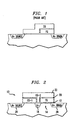
- the process for making the novel device 10 includes the growth of a tunnel oxide 12 on a silicon substrate 14 after conventional IC isolation and active area definition steps have been finished.
- the thickness of the tunnel oxide is from 50-150A and preferably between about 80-100A.
- An in-situ doped polysilicon layer, poly-1, (or other conductor) 16 is then deposited.
- the poly-1 is then patterned by means of a thick gate photoresist (PR-1), as shown in Fig 3A and the device is etched to form the individual, separated FG and CG-1 structures as shown in Fig. 3B.
- PR-1 thick gate photoresist
- An optional N + ion implant 18 in the silicon wafer substrate 14 in the region of the separation between CG-1 and FG is preferably performed.
- the resist, PR-1, used for implantation is removed, the tunnel oxide etched, and an interpoly dielectric layer 20 is deposited on the wafers to isolate the poly-1 CG-1 and FG structures from the subsequently deposited poly-2 layer 22.
- the interpoly dielectric layer 20 can be made of silicon dioxide, an ONO (oxide/nitride/oxide) composite or a known high K dielectric to achieve the necessary coupling.
- the interpoly layer 20 is from 50-300A thick and and generally about 180A thick for a silicon oxide layer.
- the thickness of the interpoly layer 20 depends upon the material employed for that layer.
- the dielectric may be removed from selected areas where a gate-dielectric thinner than the high voltage dielectric may be needed, e.g. for embedded applications, analogous to the thick gate operation.
- a disposable hard mask 24 is deposited over the poly-2 layer 22.
- a gate photoresist, PR-2 is then deposited over the hard mask 24 so as to define the width of the split gate cell and the device is etched, stopping after the poly-2 layer 22.
- the core CMOS area is protected with a photoresist (not shown), and the memory cell area is opened for a gate stack etch.
- a source/drain halo ion implant 26 is then implanted, followed by a heavy dose source/drain arsenic ion implant 28 resulting in the structure shown in Fig. 5B.
- Boron, boron fluoride or any other P-type dopant, implanted preferably with a large tilt angle can be used for the drain halo implant 26.
- an assymetric device with, for example, a halo implant in the drain end only.
- Such assymetric device generally exhibits a higher read current and has a higher speed as compared with the symmetrical device depicted in the Figures.
- CMOS processing is completed, and the hard-mask 24 is removed as part of the core CMOS process to arrive at the novel device represented by Fig. 2.
- the device With contacts open to drain, source, CG-1 and CG-2, the device may be used as a NVRAM for low voltage operation. Also, it may be noted that the process sequence allows one to use thicker oxides, formed by the composite of deposited HTO and grown oxide, for use in high voltage devices.
- a preferred process for making a small space between FG and CG-1 is shown with reference to Figs. 6-8.
- the process comprises growing the tunnel oxide 12, depositing the poly-1 layer 16, depositing a thin undoped silicon oxide dopant mask layer 30 followed by the deposition of a disposable doped oxide layer 32, e.g. a boron-phosphorous silicate glass (BPTEOS).
- BPTEOS boron-phosphorous silicate glass
- a patterned photoresist layer 34 is provided and the device is etched removing the exposed portion of the doped oxide layer 32 and undoped oxide mask layer 30 stopping at poly-1. This results in the structure shown in Fig. 6.
- the photoresist 34 is then removed, the surface is cleaned and a disposable oxide dopant mask 36 is grown/deposited.
- a BPTEOS spacer oxide 38 is deposited and a timed spacer etch is performed to reach the structure of Fig. 7. Finally, the poly-1 layer 16 is etched to form the separated CG-1 and FG areas. As previously indicated and as shown in Fig. 8, a N-type dopant (e.g. AS) is implanted in the space between the CG-1 and FG areas. Thereafter, the disposable oxide is etched away in an ammonium hydroxide/hydrogen peroxide bath. Device formation may then proceed essentially as described above with reference to Figs. 4A, 4B ,5A and 5B.
- a N-type dopant e.g. AS
- the control gates, CG-1 and CG-2 are made of the same polysilicon and are physically connected. Also, the thickness of the tunneling oxides under the FG and CG gates are generally different, making fabrication more complex.
- a large voltage ( ⁇ 7.5V) on the control gate to achieve programming in a short time ( ⁇ a few 10's of ⁇ s). This however does not allow one to scale the underlying select-gate oxide.
- the voltage on CG-1 can be limited to ⁇ 5V so that one can use the tunnel oxide as the gate of the select-gate oxide.
- the coupling ratio between the CG-2 and the CG-1 can be high, e.g. ⁇ 0.6, which is approximately similar to the coupling between CG-2 and FG.
- CG-2 e.g. ⁇ 5.0V
- the node CG-2 is electrically floated and the voltage on CG-1 is brought up, e.g. to ⁇ 5V.
- the coupling between CG-1 and CG-2 is about 0.6 so the voltage on CG-2 is increased to ⁇ 8V.
- the drain may be pulsed to initiate hot carrier generation and injection into the FG.
- Another advantage of using the structure of this invention is that the vertical field in the injection region can be independent of the select-gate voltage. Thus, if one chooses, one can apply a large voltage to CG-2 to increase the vertical field and at the same time apply a small voltage to CG-1 to limit programming current and thus improve injection efficiency, as is done in source side injection cells. Such a programming scheme allows one to conserve power in low power applications.
- ERASURE In a conventional split gate device, during erase a large negative voltage is applied to CG-2 and the drain is held at a large positive voltage. Such a scheme is also possible in the structure of the present invention. With CG-1 open and CG-2 at a negative voltage a positive drain voltage can duplicate the erase of a conventional split gate cell. However, the present cell offers the option of using a lower voltage charge pump and using the built-in charge pump for erase, in a manner analogous to programming but with negative voltages.
- channel erase is difficult to achieve due to the large coupling ratio between the substrate and FG. Due to this coupling one needs very large substrate voltages, e.g. >15V, to initiate tunneling from the floating gate to the substrate. This voltage appears across the select gate oxide and in order to prevent dielectric breakdown, thicker oxides than those required in the device of the present invention would be required. However, such thicker oxides degrade device performance. In contrast, one can readily utilize a channel erase in the present invention. Here, even if 15 volts is applied to the substrate, one can hold CG1 at 7.5V, with CG2 at 0V and thus the fields across the oxides in the select gate region is ⁇ 7.5V in all cases.
- substrate voltages e.g. >15V
- READ Read of the devices can follow in a normal fashion with the exception that during read, both CG1 and CG-2 are brought up to the wordline voltage.
- the effective capacitance of the wordline is thus similar in value to what it would be for a conventional split gate device (with a thinner gate oxide). With a thinner select-gate oxide (cf. to a conventional split gate cell), a higher on-current and thus a higher read speed is to be expected.
Landscapes
- Non-Volatile Memory (AREA)
- Semiconductor Memories (AREA)
Abstract
Description
Claims (10)
- A method of fabricating a split gate memory cell device comprising forming a tunnel oxide layer on a silicon substrate, forming a first conductive layer over said tunnel oxide layer, etching a trench in said conductive layer to divide said conductive layer into two separate layers with a space therebetween, one such layer to become a first gate electrode and the other separate layer to become a floating gate electrode of the device, forming a dielectric layer over the exposed surfaces, and depositing a second conductive layer which will become a second control gate electrode over said dielectric layer.
- The method recited in claim 1 further comprising the step of forming a highly doped ion-implant region in said substrate below said trench, subsequent to forming the floating gate electrode and prior to depositing the second conductive layer.
- The method set forth in claim 1 further comprising the steps of forming a hard mask over said second conductive layer, applying a photoresist mask over a portion of the hard mask including the area above the trench, etching the layers not protected by the photoresist so as to define the width of the device electrodes, and implanting source and drain regions in the substrate.
- The method recited in claim 1 wherein the first and second conductive layers are comprised of polysilicon.
- The method recited in claim 4 wherein the second conductive layer is silicided.
- The method recited in claim 4 wherein the tunnel oxide and the dielectric layers comprise silicon dioxide.
- The method recited in claim 2 further wherein the first and second conductive layers comprise polysilicon and said ion implanted regions are of the n+-type.
- The method recited in claim 2 wherein the first conductive layer is polysilicon and the trench is formed therein by forming an undoped silicon dioxide mask over the first conductive layer and a disposable doped silicon oxide layer over the undoped silicon dioxide layer, depositing a patterned photoresist layer over the doped silicon oxide layer, removing an exposed portion of the doped oxide layer and undoped silicon dioxide mask layer, stopping at the first polsysilicon layer, removing the photoresist, forming a disposable oxide dopant mask, depositing a doped spacer silicon dioxide followed by a timed spacer etch, and etching the first polysilicon layer to form the separated first control gate and floating gate electrodes having a space therebetween defined by the steps set forth herein.
- The method recited in claim 1 further including the step of forming a first p+ halo-implant region in the substrate under the edge area of the first control gate electrode and adjacent to at least an ion implanted drain region.
- The method recited in claim 9 wherein a second p+ halo-implant region is formed simultaneously with said first p+ halo-implant region under the edge area of the floating gate electrode and adjacent an ion implanted source region.
Applications Claiming Priority (4)
| Application Number | Priority Date | Filing Date | Title |
|---|---|---|---|
| US11560299P | 1999-01-12 | 1999-01-12 | |
| US115602P | 1999-01-12 | ||
| US09/460,652 US6168995B1 (en) | 1999-01-12 | 1999-12-14 | Method of fabricating a split gate memory cell |
| US460652 | 1999-12-14 |
Publications (2)
| Publication Number | Publication Date |
|---|---|
| EP1020902A2 true EP1020902A2 (en) | 2000-07-19 |
| EP1020902A3 EP1020902A3 (en) | 2002-01-23 |
Family
ID=26813372
Family Applications (1)
| Application Number | Title | Priority Date | Filing Date |
|---|---|---|---|
| EP00300131A Withdrawn EP1020902A3 (en) | 1999-01-12 | 2000-01-11 | Method of fabricating a split gate memory cell |
Country Status (3)
| Country | Link |
|---|---|
| US (1) | US6168995B1 (en) |
| EP (1) | EP1020902A3 (en) |
| JP (1) | JP2000208650A (en) |
Cited By (1)
| Publication number | Priority date | Publication date | Assignee | Title |
|---|---|---|---|---|
| FR2852735A1 (en) * | 2003-03-17 | 2004-09-24 | Samsung Electronics Co Ltd | LOCAL SONOS STRUCTURE FOR NON-VOLATILE SEMICONDUCTOR MEMORY AND METHOD OF MANUFACTURING |
Families Citing this family (15)
| Publication number | Priority date | Publication date | Assignee | Title |
|---|---|---|---|---|
| TW449919B (en) * | 1998-12-18 | 2001-08-11 | Koninkl Philips Electronics Nv | A method of manufacturing a semiconductor device |
| KR20010004990A (en) * | 1999-06-30 | 2001-01-15 | 김영환 | Flash EEPROM cell and method of manufacturing the same |
| US6261906B1 (en) * | 1999-08-03 | 2001-07-17 | Worldwide Semiconductor Manufacturing Corp. | Method for forming a flash memory cell with improved drain erase performance |
| KR100387267B1 (en) * | 1999-12-22 | 2003-06-11 | 주식회사 하이닉스반도체 | Multi-level flash EEPROM cell and method of manufacturing the same |
| US6362054B1 (en) * | 2000-03-13 | 2002-03-26 | Agere Systems Guardian Corp. | Method for fabricating MOS device with halo implanted region |
| KR100374649B1 (en) * | 2001-08-04 | 2003-03-03 | Samsung Electronics Co Ltd | Structure of semiconductor device and manufacturing method thereof |
| KR100468785B1 (en) * | 2003-02-19 | 2005-01-29 | 삼성전자주식회사 | Method of fabricating MOS Field Effect Transistor with pocket region |
| US7372091B2 (en) * | 2004-01-27 | 2008-05-13 | Micron Technology, Inc. | Selective epitaxy vertical integrated circuit components |
| US7504685B2 (en) | 2005-06-28 | 2009-03-17 | Micron Technology, Inc. | Oxide epitaxial isolation |
| US8320191B2 (en) | 2007-08-30 | 2012-11-27 | Infineon Technologies Ag | Memory cell arrangement, method for controlling a memory cell, memory array and electronic device |
| JP5562270B2 (en) * | 2011-02-22 | 2014-07-30 | 株式会社エフピコ | Packaging container |
| US9397176B2 (en) * | 2014-07-30 | 2016-07-19 | Freescale Semiconductor, Inc. | Method of forming split gate memory with improved reliability |
| US9570457B2 (en) | 2014-08-26 | 2017-02-14 | Taiwan Semiconductor Manufacturing Co., Ltd. | Method to control the common drain of a pair of control gates and to improve inter-layer dielectric (ILD) filling between the control gates |
| CN107924952A (en) * | 2015-04-24 | 2018-04-17 | Neo半导体公司 | Dual Function Hybrid Storage Unit |
| US20190207034A1 (en) * | 2017-12-28 | 2019-07-04 | Microchip Technology Incorporated | Split-Gate Memory Cell With Field-Enhanced Source Junctions, And Method Of Forming Such Memory Cell |
Family Cites Families (8)
| Publication number | Priority date | Publication date | Assignee | Title |
|---|---|---|---|---|
| JPH07120719B2 (en) * | 1987-12-02 | 1995-12-20 | 三菱電機株式会社 | Semiconductor memory device |
| JP2547622B2 (en) * | 1988-08-26 | 1996-10-23 | 三菱電機株式会社 | Nonvolatile semiconductor memory device |
| US5273923A (en) * | 1991-10-09 | 1993-12-28 | Motorola, Inc. | Process for fabricating an EEPROM cell having a tunnel opening which overlaps field isolation regions |
| JP2975824B2 (en) * | 1993-11-18 | 1999-11-10 | 三洋電機株式会社 | Nonvolatile semiconductor memory device |
| DE69413960T2 (en) * | 1994-07-18 | 1999-04-01 | Stmicroelectronics S.R.L., Agrate Brianza, Mailand/Milano | Non-volatile EPROM and flash EEPROM memory and method for its production |
| US5439838A (en) * | 1994-09-14 | 1995-08-08 | United Microelectronics Corporation | Method of thinning for EEPROM tunneling oxide device |
| US5714412A (en) * | 1996-12-02 | 1998-02-03 | Taiwan Semiconductor Manufacturing Company, Ltd | Multi-level, split-gate, flash memory cell and method of manufacture thereof |
| US5867425A (en) * | 1997-04-11 | 1999-02-02 | Wong; Ting-Wah | Nonvolatile memory capable of using substrate hot electron injection |
-
1999
- 1999-12-14 US US09/460,652 patent/US6168995B1/en not_active Expired - Lifetime
-
2000
- 2000-01-11 EP EP00300131A patent/EP1020902A3/en not_active Withdrawn
- 2000-01-12 JP JP3626A patent/JP2000208650A/en active Pending
Cited By (1)
| Publication number | Priority date | Publication date | Assignee | Title |
|---|---|---|---|---|
| FR2852735A1 (en) * | 2003-03-17 | 2004-09-24 | Samsung Electronics Co Ltd | LOCAL SONOS STRUCTURE FOR NON-VOLATILE SEMICONDUCTOR MEMORY AND METHOD OF MANUFACTURING |
Also Published As
| Publication number | Publication date |
|---|---|
| EP1020902A3 (en) | 2002-01-23 |
| US6168995B1 (en) | 2001-01-02 |
| JP2000208650A (en) | 2000-07-28 |
Similar Documents
| Publication | Publication Date | Title |
|---|---|---|
| US6764905B2 (en) | Method of manufacturing a scalable flash EEPROM memory cell with floating gate spacer wrapped by control gate | |
| KR100274491B1 (en) | Spacer Flash Cell Process | |
| US5824584A (en) | Method of making and accessing split gate memory device | |
| US6885586B2 (en) | Self-aligned split-gate NAND flash memory and fabrication process | |
| US6958513B2 (en) | Floating-gate memory cell having trench structure with ballistic-charge injector, and the array of memory cells | |
| US6458656B1 (en) | Process for creating a flash memory cell using a photoresist flow operation | |
| US6436766B1 (en) | Process for fabricating high density memory cells using a polysilicon hard mask | |
| US6168995B1 (en) | Method of fabricating a split gate memory cell | |
| GB2292008A (en) | A split gate type flash eeprom cell | |
| US20030141535A1 (en) | Fabrication method for flash memory | |
| JPH04215481A (en) | Three-dimensional contactless nonvolatile memory cell and its manufacture | |
| US6313500B1 (en) | Split gate memory cell | |
| US5620913A (en) | Method of making a flash memory cell | |
| US8334558B2 (en) | Method to fabricate self-aligned source and drain in split gate flash | |
| WO1990001804A1 (en) | Method and apparatus for forming a side wall contact in a nonvolatile electrically alterable memory cell | |
| US6025229A (en) | Method of fabricating split-gate source side injection flash memory array | |
| US6362052B1 (en) | Use of an etch to reduce the thickness and around the edges of a resist mask during the creation of a memory cell | |
| EP0612108B1 (en) | Double polysilicon EEPROM cell and corresponding manufacturing process | |
| US7145802B2 (en) | Programming and manufacturing method for split gate memory cell | |
| US6486029B1 (en) | Integration of an ion implant hard mask structure into a process for fabricating high density memory cells | |
| US6878986B2 (en) | Embedded flash memory cell having improved programming and erasing efficiency | |
| US7947607B2 (en) | Apparatus and associated method for making a virtual ground array structure that uses inversion bit lines | |
| US6127698A (en) | High density/speed nonvolatile memories with a textured tunnel oxide and a high capacitive-coupling ratio | |
| KR20000057746A (en) | Method of fabricating a split gate memory cell | |
| KR0123235B1 (en) | Flash Epirom Cell Manufacturing Method |
Legal Events
| Date | Code | Title | Description |
|---|---|---|---|
| PUAI | Public reference made under article 153(3) epc to a published international application that has entered the european phase |
Free format text: ORIGINAL CODE: 0009012 |
|
| AK | Designated contracting states |
Kind code of ref document: A2 Designated state(s): DE FR IT NL |
|
| AX | Request for extension of the european patent |
Free format text: AL;LT;LV;MK;RO;SI |
|
| PUAL | Search report despatched |
Free format text: ORIGINAL CODE: 0009013 |
|
| AK | Designated contracting states |
Kind code of ref document: A3 Designated state(s): DE FR IT NL |
|
| AX | Request for extension of the european patent |
Free format text: AL;LT;LV;MK;RO;SI |
|
| AKX | Designation fees paid | ||
| REG | Reference to a national code |
Ref country code: DE Ref legal event code: 8566 |
|
| STAA | Information on the status of an ep patent application or granted ep patent |
Free format text: STATUS: THE APPLICATION IS DEEMED TO BE WITHDRAWN |
|
| 18D | Application deemed to be withdrawn |
Effective date: 20020724 |