EP1020738A1 - Three-layer anti-reflection filn containing a first layer of binder resin with ultrafine particles - Google Patents
Three-layer anti-reflection filn containing a first layer of binder resin with ultrafine particles Download PDFInfo
- Publication number
- EP1020738A1 EP1020738A1 EP00300199A EP00300199A EP1020738A1 EP 1020738 A1 EP1020738 A1 EP 1020738A1 EP 00300199 A EP00300199 A EP 00300199A EP 00300199 A EP00300199 A EP 00300199A EP 1020738 A1 EP1020738 A1 EP 1020738A1
- Authority
- EP
- European Patent Office
- Prior art keywords
- layer
- reflection film
- transparent substrate
- refractive index
- thickness
- Prior art date
- Legal status (The legal status is an assumption and is not a legal conclusion. Google has not performed a legal analysis and makes no representation as to the accuracy of the status listed.)
- Granted
Links
Images


Classifications
-
- G—PHYSICS
- G02—OPTICS
- G02B—OPTICAL ELEMENTS, SYSTEMS OR APPARATUS
- G02B1/00—Optical elements characterised by the material of which they are made; Optical coatings for optical elements
- G02B1/10—Optical coatings produced by application to, or surface treatment of, optical elements
- G02B1/11—Anti-reflection coatings
- G02B1/111—Anti-reflection coatings using layers comprising organic materials
-
- B—PERFORMING OPERATIONS; TRANSPORTING
- B32—LAYERED PRODUCTS
- B32B—LAYERED PRODUCTS, i.e. PRODUCTS BUILT-UP OF STRATA OF FLAT OR NON-FLAT, e.g. CELLULAR OR HONEYCOMB, FORM
- B32B5/00—Layered products characterised by the non- homogeneity or physical structure, i.e. comprising a fibrous, filamentary, particulate or foam layer; Layered products characterised by having a layer differing constitutionally or physically in different parts
- B32B5/22—Layered products characterised by the non- homogeneity or physical structure, i.e. comprising a fibrous, filamentary, particulate or foam layer; Layered products characterised by having a layer differing constitutionally or physically in different parts characterised by the presence of two or more layers which are next to each other and are fibrous, filamentary, formed of particles or foamed
- B32B5/30—Layered products characterised by the non- homogeneity or physical structure, i.e. comprising a fibrous, filamentary, particulate or foam layer; Layered products characterised by having a layer differing constitutionally or physically in different parts characterised by the presence of two or more layers which are next to each other and are fibrous, filamentary, formed of particles or foamed one layer being formed of particles, e.g. chips, granules, powder
-
- B—PERFORMING OPERATIONS; TRANSPORTING
- B32—LAYERED PRODUCTS
- B32B—LAYERED PRODUCTS, i.e. PRODUCTS BUILT-UP OF STRATA OF FLAT OR NON-FLAT, e.g. CELLULAR OR HONEYCOMB, FORM
- B32B7/00—Layered products characterised by the relation between layers; Layered products characterised by the relative orientation of features between layers, or by the relative values of a measurable parameter between layers, i.e. products comprising layers having different physical, chemical or physicochemical properties; Layered products characterised by the interconnection of layers
- B32B7/02—Physical, chemical or physicochemical properties
- B32B7/023—Optical properties
-
- B—PERFORMING OPERATIONS; TRANSPORTING
- B32—LAYERED PRODUCTS
- B32B—LAYERED PRODUCTS, i.e. PRODUCTS BUILT-UP OF STRATA OF FLAT OR NON-FLAT, e.g. CELLULAR OR HONEYCOMB, FORM
- B32B37/00—Methods or apparatus for laminating, e.g. by curing or by ultrasonic bonding
- B32B37/14—Methods or apparatus for laminating, e.g. by curing or by ultrasonic bonding characterised by the properties of the layers
- B32B37/24—Methods or apparatus for laminating, e.g. by curing or by ultrasonic bonding characterised by the properties of the layers with at least one layer not being coherent before laminating, e.g. made up from granular material sprinkled onto a substrate
- B32B2037/243—Coating
-
- B—PERFORMING OPERATIONS; TRANSPORTING
- B32—LAYERED PRODUCTS
- B32B—LAYERED PRODUCTS, i.e. PRODUCTS BUILT-UP OF STRATA OF FLAT OR NON-FLAT, e.g. CELLULAR OR HONEYCOMB, FORM
- B32B2264/00—Composition or properties of particles which form a particulate layer or are present as additives
- B32B2264/10—Inorganic particles
Definitions
- the present invention relates to an anti-reflection film which is used for display devices and the like.
- an anti-reflection film has been disposed on a screen of a display device to improve image quality.
- Japanese Patent Application Laid-Open No. Hei 5-173001 discloses an anti-reflection film in which a first layer having a refractive index of 1.63 to 1.75 which is formed of CeO 2 and MgO, a second layer which is formed of TiO 2 and TiO, and a third layer which is formed of MgF 2 or SiO 2 are laminated in order.
- Japanese Patent Application Laid-Open No. Hei 10-300902 discloses an anti-reflection film composed of three layers whose refractive indexes are selected from the range of 1.40 to 2.20.
- the anti-reflection film disclosed in Japanese Patent Application Laid-Open No. Hei 5-173001 can exhibit an anti-reflection effect only in a narrow wavelength range and the effect is not satisfactory.
- the anti-reflection film disclosed in Japanese Patent Application Laid-Open No. Hei 10-300902 can exhibit an anti-reflection effect in a relatively wide wavelength range.
- a first layer of this anti-reflection film has a fine undulatory surface.
- anti-reflection effect as high as shown in the examples can not be exhibited when a fine undulatory surface is not formed.
- the anti-reflection effect at a wavelength of about 550 nm which exerts influence upon visibility most strongly, has not been satisfactory.
- an anti-reflection film having low reflectivity in a wide wavelength range As a result, they have found that an effective anti-reflection effect throughout the wavelength range of the visible rays can be attained by making up an anti-reflection film comprising a transparent substrate, a first layer having a refractive index of 1.70 to 1.80 and an optical thickness of 0.21 ⁇ to 0.29 ⁇ , a second layer having a refractive index of not less than 2.20 and an optical thickness of 0.41 ⁇ to 0.54 ⁇ and a third layer having a refractive index of 1.44 to 1.49 and an optical thickness of 0.22 ⁇ to 0.27 ⁇ , wherein the first layer, the second layer and the third layer are laminated on a surface of the transparent substrate in this order from the transparent substrate side toward the air layer side.
- the present invention provides an anti-reflection film comprising a transparent substrate, a first layer, a second layer and a third layer,
- the present invention also provides an anti-reflection film comprising a transparent substrate, a first layer, a second layer and a third layer,
- the present invention further provides an anti-reflection film comprising a transparent substrate, a first layer, a second layer and a third layer,
- the present invention further provides methods of producing these anti-reflection films.
- the present invention further provides a polarizing film having these anti-reflection films, an optical filter having these anti-reflection films and a liquid crystal display device having these anti-reflection films.
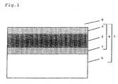
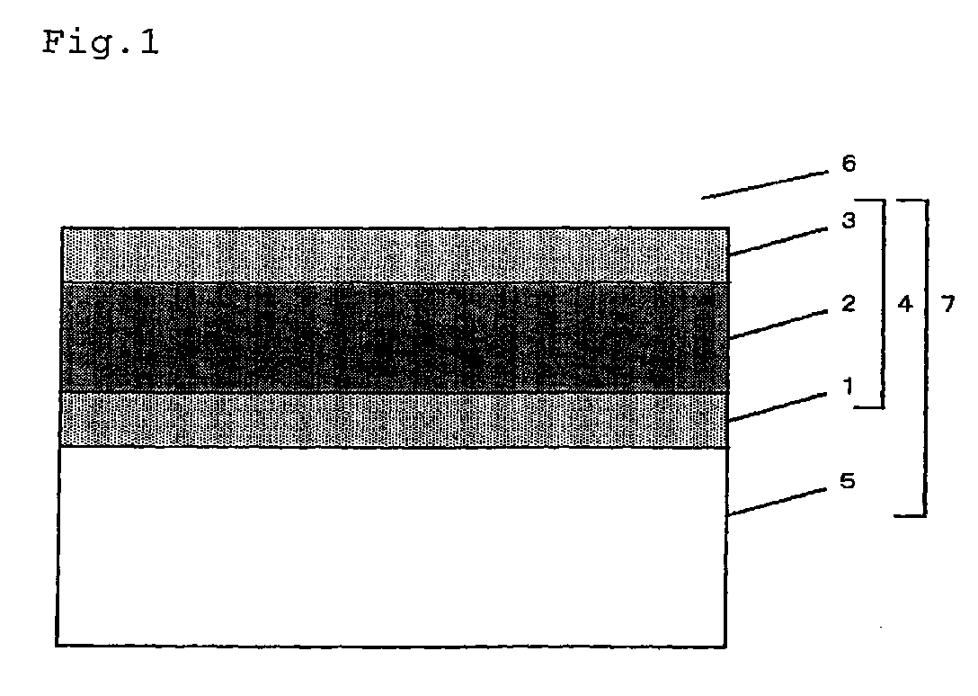
- Fig. 1 is a schematic cross section of the anti-reflection films of the present invention.
- an anti-reflection substrate (4) on a surface of a transparent substrate (5), is formed an anti-reflection substrate (4) in which a first layer (1), a second layer (2) and a third layer (3) are laminated in this order from the transparent substrate side toward the air layer side (6).
- the transparent substrate (5) used for the anti-reflection film of the present invention may have a flat form such as a plate form, a film form and a sheet form, or may be one having a curved surface such as a lens.
- transparent polymer films or sheets inorganic transparent substrates can be used.
- films and sheets of transparent polymers such as cellulose polymers (e.g., polymer of diacetylcellulose, triacetylcellulose (TAC), propionylcellulose, butyrylcellulose, acetylpropionylcellulose, nitrocellulose and acetatebutylatecellulose), polycarbonate polymers, polyarylate polymers, polyester polymers (e.g., polyethylene terephthalate (PET), polyethylenenaphthalate, polybutyleneterephthalate, poly-1,4-cyclohexanedimethyleneterephthalate and polyethylene-1,2-diphenoxyethane-4,4 -dicarboxylate), acrylic polymers (e.g., polymethylmethacrylate and poly(meth)acrylonitrile), functional norbornene polymers (e.g., ARTON® manufactured by JSR Co.
- transparent polymers such as polymer of diacetylcellulose, triacetylcellulose (TAC
- polyolefin polymers e.g., polyethylene, polypropylene, polymethylpentene, amorphous polyolefins and ZEONEX® manufactured by Nippon Zeon Co. ,Ltd.
- polyurethane polymers e.g., polyamide polymers (e.g., aromatic polyamides), polysulfone, polyethersulfone, polyetherketone, polyetherimide, polyimide, polystyrene, polyoxyethylene, polyether films, polyvinyl alcohol, fluoro polymers (e.g., poly-4-fluoroethylene and polyvinylfluoride), polyvinylchloride and polyvinylacetal, and inorganic transparent substrates such as quartz glass, alkaline glass and sapphire.
- polyamide polymers e.g., aromatic polyamides
- polysulfone e.g., polyethersulfone, polyetherketone, polyetherimide, polyimide, polystyrene
- plastic lens, glass lens and the like also can be used as a substrate.
- a refractive index of the transparent substrate to be used preferably is, but is not particularly limited to, 1.48 to 1.60.
- Polarizing films, optical filters for display devices such as CRTs and optical components such as touch panels may be used as the transparent substrate.
- the transparent substrate may have an intermediate layer on its surface in order to improve adhesion with the first layer (1) or to improve its hardness.
- the intermediate layer may be a polymer film formed of a polymer such as acrylic resin, urethane resin, silicon resin, cardo resin and polysilazane.
- the layers formed of SiO x , Al 2 O 3 or the like and layers formed of Cr, which have the thickness of about 3 nm (30 ⁇ ) to 20 nm (200 ⁇ ), may be employed.
- the transparent substrate may be provided with a fine undulation on its surface to be invested with anti-glaring property.
- the substrate may be provided with a resin layer in which silica gel, resin beads, glass beads or the like are dispersed, or may be subjected to etching, matting or the like to its surface.
- the transparent substrate may be subjected to surface treatment to its surface in order, for example, to be invested with adhesion.
- surface treatment include heating in vacuum, corona treatment, ion-bombardment, plasma treatment, ultraviolet irradiation, electron beam irradiation and the like.
- a refractive index of the first layer (1) is about 1.70 to 1.80, preferably is about 1.72 to 1.80, and more preferably is about 1.73 to 1.78.
- the refractive index is a value determined at a wavelength of 632.8 nm. In the following description, that term has the same meaning as mentioned above.
- the first layer usually has a transmittance in the visible rays range of not less than 80%.
- the first layer may, for example, be a layer formed of an inorganic dielectric.
- the inorganic dielectric include oxides comprising both an element capable of providing a low-refractive-index material and an element capable of providing a high-refractive-index material, and concretely include a mixture of a low-refractive-index material and a high-refractive-index material, a compound oxide of both an element capable of providing a low-refractive-index material and an element capable of providing a high-refractive-index material.
- Such an element capable of providing a low-refractive-index material may be Si, Al, W and the like, which may be of one kind or of two or more kinds.
- Such an element capable of providing a high-refractive-index material may be Bi, Mo, Ta, Zn, Ti, Nb, In, Zr, Sn and the like, which may be of one kind or of two or more kinds.
- Examples of such a low-refractive-index material include oxides such as SiO 2 , Al 2 O 3 and WO 3 .
- Examples of such a high-refractive-index material include oxides such as TiO 2 , Nb 2 O 5 and Ta 2 O 5 .
- Preferred mixtures of a low-refractive-index material and a high-refractive-index material include a mixture of SiO 2 and Nb 2 O 5 , a mixture of Al 2 O 3 and Nb 2 O 5 , a mixture of Al 2 O 3 and TiO 2 ,a mixture of SiO 2 and TiO 2 , and the like.
- the low-refractive-index material and the high-refractive-index material may be either crystalline or amorphous. Appropriate selection of a ratio of amounts of a low-refractive-index material and a high-refractive-index material can attain a desired refractive index.
- a compound oxide of both an element capable of providing a low-refractive-index material and an element capable of providing a high-refractive-index material may, for example, be compound oxides of Si and/or Al and Ti and/or Nb, concretely a compound oxide of Si and Nb, a compound oxide of Al and Nb, a compound oxide of Al and Ti, a compound oxide of Si and Ti, and the like. These compound oxides may be either crystalline or amorphous. Appropriate selection of a ratio of the numbers of atoms of elements capable of providing a low-refractive-index material and elements capable of providing a high-refractive-index material can attain a desired refractive index.
- the first layer may also be a layer formed by coating a coating composed of a binder and ultra-fine particles having a refractive index of not less than 1.5.
- the binder include thermosetting resins and resins hardened by radiation.
- binder ones having an acrylate type functional group are preferred.
- a binder which contain the following materials in a relatively large amount are used: relatively low molecular weight polyester; polyether; acrylic resin; epoxy resin; polyurethane; alkyd resin; spiroacetal resin; polybutadiene; polythiolpolyene resin; oligomers or preoligomers of (meth)acrylates (henceforth, acrylates and methacrylates are referred to as (meth)acrylates) of polyfunctional compounds such as polyhydric alcohol and the like; reactive diluents such as ethyl(meth)acrylate and ethylhexyl(meth)acrylate; polymers of monofunctional monomer such as styrene, vinyltoluene and N-vinylpyrrolidone; and polymers of polyfunctional monomer such as
- preferred examples include styrene derivatives (1,4-divinylbenzene, 4-vinylbenzoic acid-2-acryloylethylester, 1,4-divinylcyclohexanone and the like), vinylsulfones (divinylsulfone and the like), acrylamides (methylenebisacrylamide and the like), methacrylamides and polyfunctional epoxy compounds including Denacol® EX-313 and Denacol® EX-521 (both manufactured by Nagase Chemicals, Ltd.) and the like.
- bifunctional acrylate compound UV-8000B; manufactured by The Nippon Synthetic Chemical Industry Co., Ltd.
- UV-8000B UV-8000B
- the Nippon Synthetic Chemical Industry Co., Ltd. having an isocyanate group in one molecule preferably are used.
- a photopolymerization initiator such as acetophenones, benzophenones, Michler's benzoylbenzoate, ⁇ -amyloxime esters and thioxanthones, or a photosensitizer such as n-butylamine, triethylamine or tri-n-butylphosphine therein.
- Concrete examples include tetramethoxysilane, tetraethoxysilane, tetra-iso-propoxysilane, tetra-n-propoxysilane, tetra-n-butoxysilane, tetra-sec-butoxysilane, tetra-tert-butoxysilane, tetrapentaethoxysilane, tetrapenta-iso-propoxysilane, tetrapenta-n-propoxysilane, tetrapenta-n-butoxysilane, tetrapenta-sec-butoxysilane, tetrapenta-tert-butoxysilane, methyltrimethoxysilane, methyltriethoxysilane, methyltripropoxysilane, methyltributoxysilane, dimethyldimethoxysilane, dimethyldiethoxysilane, dimethylmethoxysilane, dimethylethoxys
- the preceding ultra-fine particles are selected from at least one kind of ultra-fine particles selected from ZnO, TiO 2 , Sb 2 O 5 , SnO 2 , ITO, Y 2 O 3 , La 2 O 3 , Al 2 O 3 , Hf 2 O 3 , Nb 2 O 5 , Bi 2 O 3 , Ta 2 O 5 , MoO 3 , CeO 2 and ZrO 2 .
- the ultra-fine particles desirably have an average particle size of about 5 to 50 nm.
- the first layer formed by coating a coating composed of a binder and ultra-fine particles having a refractive index of not less than 1.5 may have a fine undulatory surface.
- a variety of methods can be utilized for forming a fine undulatory surface. Non-limiting examples of methods for forming a fine undulatory surface will be described below.
- the first layer has an optical thickness of about 0.21 ⁇ to 0.29 ⁇ , preferably about 0.22 ⁇ to 0.28 ⁇ , and more preferably about 0.23 ⁇ to 0.27 ⁇ .
- ⁇ used herein is a preset wavelength. When it is used for display devices such as liquid crystal display devices, it is arbitrarily set in the wavelength range of the visible rays, and it is usually set to 550 nm. In the following description, that term has the same meaning as mentioned above.
- the optical thickness of a layer is the product of the layer thickness and the refractive index.
- a thickness of the first layer usually is in the range of about 60 nm to 95 nm.
- the second layer (2) has a refractive index of not less than about 2.20, preferably not less than 2.25.
- a transmittance of the second layer in the visible rays range is usually not less than 80%.
- the second layer may, for example, be a layer formed of an inorganic dielectric, and preferably is a layer composed mainly of Nb oxide and Ti oxide from the viewpoints of a material cost and a deposition rate.
- the second layer has an optical thickness of about 0.41 ⁇ to 0.54 ⁇ , preferably about 0.43 ⁇ to 0.53 ⁇ , more preferably about 0.45 ⁇ to 0.52 ⁇ .
- a thickness of the second layer usually is in the range of about 90 nm to 125 nm.
- the third layer (3) has a refractive index of about 1.44 to 1.49.
- a transmittance of the third layer in the visible rays range is usually not less than 80%.
- the third layer may, for example, be a layer formed of an inorganic dielectric, and preferably is a layer composed mainly of Si oxide from the viewpoints of surface hardness and ease of investing water and oil repellency.
- the third layer has an optical thickness of about 0.22 ⁇ to 0.27 ⁇ , preferably about 0.23 ⁇ to 0.26 ⁇ .
- a thickness of the third layer is usually in the range of about 80 nm to 100 nm.
- these layers can be disposed on the transparent substrate by known methods including physical vapor deposition (PVD) methods such as the electron beam evaporation method, the induction heating evaporation method, the resistance heating evaporation method, the ion plating method and the sputtering method, the plasma chemical vapor deposition (CVD) method, and a coating method in which an alkoxide solution or the like is applied.
- PVD physical vapor deposition
- CVD plasma chemical vapor deposition
- a layer formed of a mixture can be formed on the transparent substrate by a dual-source evaporation method in which at least two kinds of evaporating materials are evaporated from separate evaporation sources and a mixed coating is formed, a vacuum evaporation method or sputtering method using a mixed material of two kinds of inorganic dielectric, or the like.
- the layer formed of a mixture can also be formed on the surface of the transparent substrate by a sputtering method using an alloy target of two kinds of metals.
- a sputtering method using an alloy target of two kinds of metals it can be formed by a sputtering method using a sputtering target containing at least one element selected from Si, Al, W and the like and at least one element selected from Bi, Mo, Ta, Zn, Ti, Nb, In, Zr, Sn and the like.
- the sputtering target may be either an alloy target or an oxide target, but the alloy target is preferred because the first layer can be formed by DC magnetron sputtering.
- a ratio of the number of Si atom to the sum of the numbers of Si atom and Ti atom in the alloy target, which is represented as Si/(Si+Ti), is usually in the range of from 0.41 to 0.55.
- the first layer When the first layer is formed by coating a coating composed of a binder and ultra-fine particles having a refractive index of not less than 1.5, the first layer can be formed on the transparent substrate by coating methods such as air doctor coating, blade coating, knife coating, reverse coating, transfer roll coating, gravure roll coating, kiss coating, cast coating, spray coating, slot orifice coating, calender coating, electro-deposition coating, dip coating and die coating, and printing method including relief printing process such as flexographic printing, intaglio printing process such as direct gravure printing and offset gravure printing, plano printing process such as offset printing, stencil printing process methods such as screen printing.
- coating methods such as air doctor coating, blade coating, knife coating, reverse coating, transfer roll coating, gravure roll coating, kiss coating, cast coating, spray coating, slot orifice coating, calender coating, electro-deposition coating, dip coating and die coating, and printing method including relief printing process such as flexographic printing, intaglio printing process such as direct gravure printing and offset gravure printing, plano printing
- the coating contains a solvent
- that layer is formed by performing a drying step and subsequently hardening the coated layer or printed layer with, for example, radiation irrdiation (in the case of using ultraviolet rays, a photopolymerization initiator is added).
- radiation is an electron beam
- an electron beam with an energy of 50 to 1000 KeV can be used, which is emitted from a variety of electron beam accelerators such as ones of Cockcroft-Walton type, van de Graaff type, resonance transforming type, insulating core transformer type, linear type, Dinamitron type and high-frequency type.
- the radiation is ultraviolet rays
- a light source such as ultra-high-pressure mercury vapor lamp, high-pressure mercury vapor lamp, low-pressure mercury vapor lamp, carbon arc, xenone arc and metal halide lamp can be used.
- This anti-reflection film may be disposed on either one side or both sides of the transparent substrate.
- a smudge resistant coating layer may be formed on the anti-reflection film as necessary.
- a batch or in-line production machine can be employed in the case where the transparent substrate is in the form of a plate, sheet or lens.
- a winding-up vacuum film forming machine can also be used.
- the anti-reflection film of the present invention can be used with attached to polarizing films, retardation films, touch panels, optical filters, VDT filters, PDP front panels, projection television front panels, glasses, sunglasses, lens such as ones for a camera, telescope, microscope, projection television, etc., optical products such as prisms, CRTs (direct mounting to CRTs, film laminating, etc.), organic EL and inorganic EL display devices (film laminating, direct mounting to substrates, etc.), mirrors and the like.
- the transparent substrate with the anti-reflection film can be used for liquid crystal display devices when the substrate is a polarizing film.
- the transparent substrate with the anti-reflection film can be used with attached to the front of a variety of display devices such as CRTs, PDPs, liquid crystal displays, and organic EL and inorganic EL display devices.
- a method for placing the anti-reflection film on a polarizing film, optical filter, touch panel and the like may be one in which a transparent substrate on which an anti-reflection film has been formed is laminated onto the polarizing film, optical filter, touch panel or the like with disposing an adhesive layer as well as one in which the anti-reflection substrate (first layer, second layer and third layer) is formed directly on the polarizing film, optical filter, touch panel or the like.
- the anti-reflection film of the present invention can exhibit an excellent anti-reflection effect throughout the visible rays range, and can be produced at low cost.
- a refractive index is a value detected at a wavelength of 632.8 nm.
- an anti-reflection film (7) is produced by forming an anti-reflection substrate (4) obtained by forming successively, on the substrate (5), a first layer (1) of 83% of Al 2 O 3 and 17% of TiO 2 [a refractive index: 1.74; a thickness: 76 nm (760 ⁇ )], a second layer (2) of Nb 2 O 5 [a refractive index: 2.34; a thickness: 113 nm (1130 ⁇ )], and a third layer (3) of SiO 2 [a refractive index: 1.47; a thickness: 90 run (900 ⁇ )].
- Fig. 2 illustrates the reflection spectrum of the surface of the anti-reflection substrate of the anti-reflection film (7).
- a transparent polymer film which was used as a transparent substrate (5), was prepared by forming an about 5 ⁇ m thick acrylic resin layer on a triacetylcellulose film (the commercial name: FUJITAC SH-80; manufactured by Fuji Photo Film Co., Ltd.).
- a first layer (1) On the transparent substrate was formed a first layer (1) by the DC magnetron sputtering method under a 640-W condition using an alloy target composed of Si and Ti which had an atomic ratio, represented by Si/(Si+Ti), of 0.48 and introducing a mixed gas of argon and oxygen (the oxygen concentration was 2 parts by volume based on 100 parts by volume of the mixed gas) with adjusting a pressure in the system at the time of forming the layer to 0.666 Pa (5 ⁇ 10 -3 Torr).
- a mixed gas of argon and oxygen the oxygen concentration was 2 parts by volume based on 100 parts by volume of the mixed gas
- the refractive index of the layer on the Si substrate with an ellipsometer indicated that the layer had a refractive index of 1.77.
- a second layer (2) by the DC magnetron sputtering method under a 750-W condition using an Nb target, in which method a mixed gas of argon and oxygen (the oxygen concentration was 5.5 parts by volume based on 100 parts by volume of the mixed gas) was introduced so that a pressure in the system at the time of forming the layer becomes 0.666 Pa (5 ⁇ 10 -3 Torr).
- a mixed gas of argon and oxygen the oxygen concentration was 5.5 parts by volume based on 100 parts by volume of the mixed gas
- the refractive index of the layer on the Si substrate with an ellipsometer indicated that the layer had a refractive index of 2.28.
- Measurement of the thickness of that layer with surface profile measuring system revealed that the layer had a thickness of 111 nm (1110 ⁇ ). Accordingly, the second layer formed on the transparent substrate on which the first layer had been formed has a refractive index of 2.28 and a thickness of 111 nm (1110 ⁇ ).
- a third layer (3) by the RF magnetron sputtering method under a 500-W condition using an SiO 2 target with adjusting a pressure at the time of forming the layer to be 0.266 Pa (2 ⁇ 10 -3 Torr) by introducing argon as a coating forming gas.
- an anti-reflection substrate (4) was formed.
- an Si substrate having a mirror polished surface was placed, in the coating system, together with the transparent substrate on which the second layer had been formed. On the mirror polished surface was formed a layer similar to the third layer. Measurement of the refractive index of the layer on the Si substrate with an ellipsometer indicated that the layer had a refractive index of 1.47.
- the third layer formed on the transparent substrate on which the second layer had been formed has a refractive index of 1.47 and a thickness of 90 nm (900 ⁇ ).
- the thus formed anti-reflection film (7) was transparent.
- Fig. 3 illustrates the reflection spectrum of the surface of the anti-reflection substrate (4) of the anti-reflection film (7).
- An anti-reflection substrate (4) was formed in the same manner as Example 2 except for using, as a transparent substrate (5), a transparent polymer film composed of a triacetylcellulose film (the commercial name: FUJITAC SH-80; manufactured by Fuji Photo Film Co., Ltd.) and an about 3 ⁇ m thick anti-glaring layer formed, as an acrylic resin base material, on the triacetylcellulose film.
- a transparent polymer film composed of a triacetylcellulose film (the commercial name: FUJITAC SH-80; manufactured by Fuji Photo Film Co., Ltd.) and an about 3 ⁇ m thick anti-glaring layer formed, as an acrylic resin base material, on the triacetylcellulose film.
- the thus toned anti-reflection film (7) was transparent.
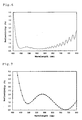
- Fig. 4 illustrates the reflection spectrum of the surface of the anti-reflection substrate (4) of the anti-reflection film (7).
- a film (PET 5; manufactured by Dai Nippon Printing Co., Ltd.) was used which was composed of a transparent substrate (5) and a first layer (1) formed by coating a coating composed of a binder and ultra-fine particles having a refractive index of not less than 1.5.
- This film had the first layer which had been formed by coating a coating composed of a binder and ultra-fine ZrO 2 particles on a polyethyleneterephthalate having an intermediate layer formed of a polymer.
- the first layer had a thickness of about 64 nm (640 ⁇ ) and a refractive index of 1.75.
- the first layer had no fine undulatory surface.
- a second and third layers were formed on the first layer of the film using a sputtering machine manufactured by Tokuda Co., Ltd. (the model CFS-8EP-55).
- the second layer On the first layer was formed the second layer by the DC magnetron sputtering method under a 750-W condition using an Nb target, in which method a mixed gas of argon and oxygen (the oxygen concentration was 5.5 parts by volume based on 100 parts by volume of the mixed gas) was introduced so that a pressure in the system at the time of forming the layer becomes 0.666 Pa (5 ⁇ 10 -3 Torr). Measurement of the refractive index and the thickness of the second layer was conducted in the same manner as in Example 2. The second layer has a refractive index of 2.30 and a thickness of 115 nm (1150 ⁇ ).
- the third layer On the second layer was subsequently formed the third layer by the RF magnetron sputtering method under a 500-W condition using an SiO 2 target with adjusting the pressure at the time of forming the layer to be 0.266 Pa (2 ⁇ 10 -3 Torr) by introducing argon as a coating forming gas.
- an anti-reflection substrate (4) was formed.
- Measurement of the refractive index and the thickness of the third layer was conducted in the same manner as in Example 2.
- the third layer has a refractive index of 1.46 and a thickness of 94 nm (940 ⁇ ).
- the thus formed anti-reflection film (7) was transparent.
- Fig. 5 illustrates the reflection spectrum of the surface of the anti-reflection substrate of the anti-reflection film (7).
- a film (PET 5; manufactured by Dai Nippon Printing Co., Ltd.) was used which was composed of a transparent substrate (5) and a first layer (1) formed by coating a coating composed of a binder and ultra-fine particles having a refractive index of not less than 1.5.
- This film was the same as the film used in Example 4 except that the thickness of the first layer was about 87 nm (870 ⁇ ).
- a second and third layers were formed on the first layer using a winding-up sputtering machine manufactured by ULVAC Co., Ltd. (SPW-130).
- the second layer On the transparent substrate having the first layer was formed the second layer by the DC magnetron sputtering method under a 30-kW condition using a Ti target, in which method a mixed gas of argon and oxygen (the oxygen concentration was 6.2 parts by volume based on 100 parts by volume of the mixed gas) was introduced so that the pressure in the system at the time of forming the layer becomes 0.133 Pa (1.0 ⁇ 10 -3 Torr).
- the second layer has a refractive index of 2.35 and a thickness of 112 nm (1120 ⁇ ).
- the third layer by the AC magnetron sputtering method under a 10-kW condition using an Si target in which a mixed gas of argon and oxygen (the oxygen concentration was 20 parts by volume based on 100 parts by volume of the mixed gas) was introduced so that the pressure in the system at the time of forming the layer becomes 0.042 Pa (3.2 ⁇ 10 -4 Torr).
- a mixed gas of argon and oxygen the oxygen concentration was 20 parts by volume based on 100 parts by volume of the mixed gas
- the third layer has a refractive index of 1.46 and a thickness of 89 nm (890 ⁇ ).
- the thus formed anti-reflection film (7) was transparent.
- Fig. 6 illustrates the reflection spectrum of the surface of the anti-reflection substrate (4) of the anti-reflection film (7).
- An anti-reflection film is obtained by using, as a transparent substrate, a transparent polymer film composed of a triacetylcellulose film (the commercial name: FUJITAC SH-80; manufactured by Fuji Photo Film Co., Ltd.) and an about 5 ⁇ m thick acrylic resin coating formed on the triacetylcellulose film and forming successively, on the substrate, a first layer which was an oxide of Si and Ti and had an atomic ratio, represented by Si/(Si+Ti), of 0.48 [a refractive index: 1.74; a thickness: 50 nm (500 ⁇ )], a second layer formed of Nb 2 O 5 [a refractive index: 2.34; a thickness: 125 nm (1250 ⁇ )], and a third layer formed of SiO 2 [a refractive index: 1.47; a thickness: 90 nm (900 ⁇ )].
- Fig. 7 illustrates the reflection spectrum of the surface of the anti-reflection substrate of the anti-reflection film.
- An anti-reflection film is obtained by using, as a transparent substrate, a transparent polymer film composed of a triacetylcellulose film (the commercial name: FUJITAC SH-80; manufactured by Fuji Photo Film Co., Ltd.) and an about 5 ⁇ m thick acrylic resin coating formed on the triacetylcellulose film and forming successively, on the substrate, a first layer which was an oxide of Si and Ti and had an atomic ratio, represented by Si/(Si+Ti), of 0.48 [a refractive index: 1.74; a thickness: 73 nm (730 ⁇ )], a second layer formed of La 2 O 3 [a refractive index: 1.90; a thickness: 111 nm (1110 ⁇ )], and a third layer formed of SiO 2 [a refractive index: 1.47; a thickness: 90 nm (900 ⁇ )].
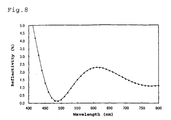
- Fig. 8 illustrates the reflection spectrum of the surface of the anti-reflection substrate of the anti-reflection film.
Landscapes
- Physics & Mathematics (AREA)
- General Physics & Mathematics (AREA)
- Optics & Photonics (AREA)
- Laminated Bodies (AREA)
- Surface Treatment Of Optical Elements (AREA)
Abstract
wherein the first layer, the second layer and the third layer are laminated on a surface of the transparent substrate in this order from the transparent substrate side toward the air layer side, and λ is equal to 550 nm.
Description
- The present invention relates to an anti-reflection film which is used for display devices and the like.
- Heretofore, many display devices, such as a cathode-rays tube(CRT), a liquid crystal display device, a plasma display panel(PDP), an organic electroluminescence(EL) device and an inorganic EL display device, has been used under environment, both indoor and outdoor, where outdoor light comes onto a screen of a display device. There has been a problem that incident rays are reflected on the surface, so that images in the screen becomes difficult to be seen.
- As a solution to this problem, an anti-reflection film has been disposed on a screen of a display device to improve image quality.
- For example, Japanese Patent Application Laid-Open No. Hei 5-173001 discloses an anti-reflection film in which a first layer having a refractive index of 1.63 to 1.75 which is formed of CeO2 and MgO, a second layer which is formed of TiO2 and TiO, and a third layer which is formed of MgF2 or SiO2 are laminated in order.
- Japanese Patent Application Laid-Open No. Hei 10-300902 discloses an anti-reflection film composed of three layers whose refractive indexes are selected from the range of 1.40 to 2.20.
- However, the anti-reflection film disclosed in Japanese Patent Application Laid-Open No. Hei 5-173001 can exhibit an anti-reflection effect only in a narrow wavelength range and the effect is not satisfactory. On the other hand, the anti-reflection film disclosed in Japanese Patent Application Laid-Open No. Hei 10-300902 can exhibit an anti-reflection effect in a relatively wide wavelength range. However, a first layer of this anti-reflection film has a fine undulatory surface. In general, anti-reflection effect as high as shown in the examples can not be exhibited when a fine undulatory surface is not formed. In addition, even though a fine undulatory surface is formed, the anti-reflection effect at a wavelength of about 550 nm, which exerts influence upon visibility most strongly, has not been satisfactory.
- In other-words, no anti-reflection film which can exhibit sufficient anti-reflection effect throughout the wavelength range of the visible rays has not yet been known.
- Under these circumstances, the present inventors have intensively studied to develop an anti-reflection film having low reflectivity in a wide wavelength range. As a result, they have found that an effective anti-reflection effect throughout the wavelength range of the visible rays can be attained by making up an anti-reflection film comprising a transparent substrate, a first layer having a refractive index of 1.70 to 1.80 and an optical thickness of 0.21 λ to 0.29 λ, a second layer having a refractive index of not less than 2.20 and an optical thickness of 0.41 λ to 0.54 λ and a third layer having a refractive index of 1.44 to 1.49 and an optical thickness of 0.22 λ to 0.27 λ, wherein the first layer, the second layer and the third layer are laminated on a surface of the transparent substrate in this order from the transparent substrate side toward the air layer side.
- That is, the present invention provides an anti-reflection film comprising a transparent substrate, a first layer, a second layer and a third layer,
- a first layer having a refractive index of 1.70 to 1.80 and an optical thickness of 0.21 λ to 0.29 λ,
- a second layer having a refractive index of not less than 2.20 and an optical thickness of 0.41 λ to 0.54 λ,
- a third layer having a refractive index of 1.44 to 1.49
and an optical thickness of 0.22 λ to 0.27 λ,
wherein the first layer, the second layer and the third layer are laminated on a surface of the transparent substrate in this order from the transparent substrate side toward the air layer side. -
- The present invention also provides an anti-reflection film comprising a transparent substrate, a first layer, a second layer and a third layer,
- a first layer having a thickness of 60 nm to 95 nm which is a layer formed of a mixture of oxides or a compound oxide of at least one kind of element selected from the group consisting of Si, Al and W and at least one kind of element selected from the group consisting of Bi, Mo, Ta, Zn, Ti, Nb, In, Zr and Sn,
- a second layer having a thickness of 90 nm to 125 nm which is a layer formed of an oxide of at least one kind of element selected from the group consisting of Ti and Nb,
- a third layer having a thickness of 80 nm to 100 nm which
is formed of an oxide of Si,
wherein the first layer, the second layer and the third layer are laminated on a surface of the transparent substrate in this order from the transparent substrate side toward the air layer side. -
- The present invention further provides an anti-reflection film comprising a transparent substrate, a first layer, a second layer and a third layer,
- a first layer having a thickness of 60 nm to 95 nm which is a layer formed of a binder and ultra-fine particles having a refractive index of not less than 1.5,
- a second layer having a thickness of 90 nm to 125 nm which is a layer formed of an oxide of at least one kind of element selected from the group consisting of Ti and Nb,
- a third layer having a thickness of 80 nm to 100 nm which
is formed of an oxide of Si,
wherein the first layer, the second layer and the third layer are laminated on a surface of the transparent substrate in this order from the transparent substrate side toward the air layer side. -
- The present invention further provides methods of producing these anti-reflection films.
- The present invention further provides a polarizing film having these anti-reflection films, an optical filter having these anti-reflection films and a liquid crystal display device having these anti-reflection films.
- Further scope of applicability of the present invention will become apparent from the detailed description given hereinafter. However, it should be understood that the detailed description and specific examples, while indicating preferred embodiments of the invention, are given by way of illustration only, since various changes and modifications within the spirit and scope of the invention will become apparent to those skilled in the art from this detailed description.
- The present invention will become more fully understood from the detailed description given herein below and accompanying drawings which are given by way of illustration only, and thus are not limitative of the present invention and wherein;
- Fig. 1 is a schematic view which illustrates a cross section of the anti-reflection film of the present invention.
- Fig. 2 illustrates the reflection spectrum of the surface of the anti-reflection substrate of the anti-reflection film which is obtained in Example 1.
- Fig. 3 illustrates the reflection spectrum of the surface of the anti-reflection substrate of the anti-reflection film which was obtained in Example 2.
- Fig. 4 illustrates the reflection spectrum of the surface of the anti-reflection substrate of the anti-reflection film which was obtained in Example 3.
- Fig. 5 illustrates the reflection spectrum of the surface of the anti-reflection substrate of the anti-reflection film which was obtained in Example 4.
- Fig. 6 illustrates the reflection spectrum of the surface of the anti-reflection substrate of the anti-reflection film which was obtained in Example 5.
- Fig. 7 illustrates the reflection spectrum of the surface of the anti-reflection substrate of the anti-reflection film which is obtained in Comparative Example 1.
- Fig. 8 illustrates the reflection spectrum of the surface of the anti-reflection substrate of the anti-reflection film which is obtained in Comparative Example 2.
-
- The present invention will be explained in detail below.
- Fig. 1 is a schematic cross section of the anti-reflection films of the present invention.
- In an anti-reflection film (7) of the present invention, on a surface of a transparent substrate (5), is formed an anti-reflection substrate (4) in which a first layer (1), a second layer (2) and a third layer (3) are laminated in this order from the transparent substrate side toward the air layer side (6).
- The transparent substrate (5) used for the anti-reflection film of the present invention may have a flat form such as a plate form, a film form and a sheet form, or may be one having a curved surface such as a lens.
- As such a transparent substrate, known transparent polymer films or sheets, inorganic transparent substrates can be used. Concrete examples thereof include films and sheets of transparent polymers such as cellulose polymers (e.g., polymer of diacetylcellulose, triacetylcellulose (TAC), propionylcellulose, butyrylcellulose, acetylpropionylcellulose, nitrocellulose and acetatebutylatecellulose), polycarbonate polymers, polyarylate polymers, polyester polymers (e.g., polyethylene terephthalate (PET), polyethylenenaphthalate, polybutyleneterephthalate, poly-1,4-cyclohexanedimethyleneterephthalate and polyethylene-1,2-diphenoxyethane-4,4-dicarboxylate), acrylic polymers (e.g., polymethylmethacrylate and poly(meth)acrylonitrile), functional norbornene polymers (e.g., ARTON® manufactured by JSR Co. ,Ltd.) polyolefin polymers (e.g., polyethylene, polypropylene, polymethylpentene, amorphous polyolefins and ZEONEX® manufactured by Nippon Zeon Co. ,Ltd.), polyurethane polymers, polyamide polymers (e.g., aromatic polyamides), polysulfone, polyethersulfone, polyetherketone, polyetherimide, polyimide, polystyrene, polyoxyethylene, polyether films, polyvinyl alcohol, fluoro polymers (e.g., poly-4-fluoroethylene and polyvinylfluoride), polyvinylchloride and polyvinylacetal, and inorganic transparent substrates such as quartz glass, alkaline glass and sapphire. In addition, plastic lens, glass lens and the like also can be used as a substrate. A refractive index of the transparent substrate to be used preferably is, but is not particularly limited to, 1.48 to 1.60. Polarizing films, optical filters for display devices such as CRTs and optical components such as touch panels may be used as the transparent substrate.

- The transparent substrate may have an intermediate layer on its surface in order to improve adhesion with the first layer (1) or to improve its hardness. The intermediate layer may be a polymer film formed of a polymer such as acrylic resin, urethane resin, silicon resin, cardo resin and polysilazane. In addition, the layers formed of SiOx, Al2O3 or the like and layers formed of Cr, which have the thickness of about 3 nm (30 Å) to 20 nm (200 Å), may be employed.
- The transparent substrate may be provided with a fine undulation on its surface to be invested with anti-glaring property. For the transparent substrate to be invested with the anti-glaring property, the substrate may be provided with a resin layer in which silica gel, resin beads, glass beads or the like are dispersed, or may be subjected to etching, matting or the like to its surface.
- The transparent substrate may be subjected to surface treatment to its surface in order, for example, to be invested with adhesion. Examples of such surface treatment include heating in vacuum, corona treatment, ion-bombardment, plasma treatment, ultraviolet irradiation, electron beam irradiation and the like.
- A refractive index of the first layer (1) is about 1.70 to 1.80, preferably is about 1.72 to 1.80, and more preferably is about 1.73 to 1.78. The refractive index is a value determined at a wavelength of 632.8 nm. In the following description, that term has the same meaning as mentioned above.
- The first layer usually has a transmittance in the visible rays range of not less than 80%.
- The first layer may, for example, be a layer formed of an inorganic dielectric. Examples of the inorganic dielectric include oxides comprising both an element capable of providing a low-refractive-index material and an element capable of providing a high-refractive-index material, and concretely include a mixture of a low-refractive-index material and a high-refractive-index material, a compound oxide of both an element capable of providing a low-refractive-index material and an element capable of providing a high-refractive-index material.
- Such an element capable of providing a low-refractive-index material may be Si, Al, W and the like, which may be of one kind or of two or more kinds. Such an element capable of providing a high-refractive-index material may be Bi, Mo, Ta, Zn, Ti, Nb, In, Zr, Sn and the like, which may be of one kind or of two or more kinds. Examples of such a low-refractive-index material include oxides such as SiO2, Al2O3 and WO3. Examples of such a high-refractive-index material include oxides such as TiO2, Nb2O5 and Ta2O5. Preferred mixtures of a low-refractive-index material and a high-refractive-index material include a mixture of SiO2 and Nb2O5, a mixture of Al2O3 and Nb2O5, a mixture of Al2O3 and TiO2 ,a mixture of SiO2 and TiO2, and the like. The low-refractive-index material and the high-refractive-index material may be either crystalline or amorphous. Appropriate selection of a ratio of amounts of a low-refractive-index material and a high-refractive-index material can attain a desired refractive index.
- A compound oxide of both an element capable of providing a low-refractive-index material and an element capable of providing a high-refractive-index material may, for example, be compound oxides of Si and/or Al and Ti and/or Nb, concretely a compound oxide of Si and Nb, a compound oxide of Al and Nb, a compound oxide of Al and Ti, a compound oxide of Si and Ti, and the like. These compound oxides may be either crystalline or amorphous. Appropriate selection of a ratio of the numbers of atoms of elements capable of providing a low-refractive-index material and elements capable of providing a high-refractive-index material can attain a desired refractive index.
- The first layer may also be a layer formed by coating a coating composed of a binder and ultra-fine particles having a refractive index of not less than 1.5. Examples of the binder include thermosetting resins and resins hardened by radiation.
- As the binder, ones having an acrylate type functional group are preferred. For example, a binder which contain the following materials in a relatively large amount are used: relatively low molecular weight polyester; polyether; acrylic resin; epoxy resin; polyurethane; alkyd resin; spiroacetal resin; polybutadiene; polythiolpolyene resin; oligomers or preoligomers of (meth)acrylates (henceforth, acrylates and methacrylates are referred to as (meth)acrylates) of polyfunctional compounds such as polyhydric alcohol and the like; reactive diluents such as ethyl(meth)acrylate and ethylhexyl(meth)acrylate; polymers of monofunctional monomer such as styrene, vinyltoluene and N-vinylpyrrolidone; and polymers of polyfunctional monomer such as
- trimethyrolpropanetri(meth)acrylate,
- trimethylolethanetri(meth)acrylate,
- 1,4-cyclohexanediacrylate,
- pentaerythritotetra (meth) acrylate,
- hexanediol (meth ) acrylate,
- tripropyleneglycoldi (meth ) acrylate,
- diethyleneglycoldi(meth)acrylate,
- pentaerythritoltri (meth) acrylate,
- dipentaerythritoltetra (meth) acrylate,
- dipentaerythritolpenta (meth) acrylate,
- dipentaerythritolhexa (meth) acrylate,
- 1,2,4-cyclohexanetetramethacrylate,
- 1,6-hexanedioldi(meth)acrylate,
- neopentylglycoldi(meth)acrylate and UV-6300B (manufactured by The Nippon Synthetic Chemical Industry Co., Ltd.)
-
- In addition, preferred examples include styrene derivatives (1,4-divinylbenzene, 4-vinylbenzoic acid-2-acryloylethylester, 1,4-divinylcyclohexanone and the like), vinylsulfones (divinylsulfone and the like), acrylamides (methylenebisacrylamide and the like), methacrylamides and polyfunctional epoxy compounds including Denacol® EX-313 and Denacol® EX-521 (both manufactured by Nagase Chemicals, Ltd.) and the like. Alternatively, bifunctional acrylate compound (UV-8000B; manufactured by The Nippon Synthetic Chemical Industry Co., Ltd.) having an isocyanate group in one molecule preferably are used.
- Furthermore, at the time of hardening the preceding resins hardened by radiation by using ultraviolet rays, it is preferable to use them with mixing a photopolymerization initiator such as acetophenones, benzophenones, Michler's benzoylbenzoate, α-amyloxime esters and thioxanthones, or a photosensitizer such as n-butylamine, triethylamine or tri-n-butylphosphine therein.
- Into the resins hardened by radiation can be contained the reactive organic silicon compounds represented by the following formula:
- Concrete examples include tetramethoxysilane, tetraethoxysilane, tetra-iso-propoxysilane, tetra-n-propoxysilane, tetra-n-butoxysilane, tetra-sec-butoxysilane, tetra-tert-butoxysilane, tetrapentaethoxysilane, tetrapenta-iso-propoxysilane, tetrapenta-n-propoxysilane, tetrapenta-n-butoxysilane, tetrapenta-sec-butoxysilane, tetrapenta-tert-butoxysilane, methyltrimethoxysilane, methyltriethoxysilane, methyltripropoxysilane, methyltributoxysilane, dimethyldimethoxysilane, dimethyldiethoxysilane, dimethylmethoxysilane, dimethylethoxysilane, dimethylpropoxysilane, dimethylbutoxysilane, methyldimethoxysilane, methyldiethoxysilane and hexyltrimethoxysilane.
- The preceding ultra-fine particles are selected from at least one kind of ultra-fine particles selected from ZnO, TiO2, Sb2O5, SnO2, ITO, Y2O3, La2O3, Al2O3, Hf2O3, Nb2O5, Bi2O3, Ta2O5, MoO3, CeO2 and ZrO2. The ultra-fine particles desirably have an average particle size of about 5 to 50 nm.
- About 0.1 to 20 parts by weight, per part by weight of the binder ,of the ultra-fine particles are used.
- The first layer formed by coating a coating composed of a binder and ultra-fine particles having a refractive index of not less than 1.5 may have a fine undulatory surface.
- A variety of methods can be utilized for forming a fine undulatory surface. Non-limiting examples of methods for forming a fine undulatory surface will be described below.
- Method (1): As mentioned above, a first layer having a fine undulatory surface can be formed on a transparent substrate by coating, on the transparent substrate which has a fine undulatory surface, a coating composed of a binder and ultra-fine particles having a refractive index of not less than 1.5.
- Method (2): In forming the first layer by coating a coating composed of a binder and ultra-fine particles having a refractive index of not less than 1.5 on a transparent substrate, an unhardened first layer is formed by coating the coating composed of the binder and the ultra-fine particles having a refractive index of not less than 1.5. On the unhardened first layer is laminated a mat-like forming film having a fine undulatory surface to make a fine undulatory surface in the first layer. The resulting laminate is hardened by heating and/or radiation irradiation. The forming film is removed from the hardened laminate to form the first layer with a fine undulatory surface on the transparent substrate.
- Method (3): An unhardened first layer is formed by coating a coating composed of a binder and ultra-fine particles having a refractive index of not less than 1.5 on an intermediate layer of unhardened polymer is subsequently formed on a transparent substrate. The unhardened first layer is laminated with a mat-like forming film having a fine undulatory surface. The resulting laminate is hardened by heating and/or radiation irradiation. The forming film is removed from the hardened laminate to form the first layer with a fine undulatory surface on the transparent substrate.
- Method (4): An unhardened first layer is formed by coating a coating composed of a binder and ultra-fine particles having a refractive index of not less than 1.5 on a mat-like forming film having a fine undulatory surface. The unhardened first layer is laminated with a transparent substrate. The resulting laminate is hardened by heating and/or radiation irradiation. The forming film is removed from the hardened laminate to form the first layer with a fine undulatory surface on the transparent substrate.
- Method (5): On a mat-like forming film having a fine undulatory surface, an unhardened first layer is formed by coating a coating composed of a binder and ultra-fine particles having a refractive index of not less than 1.5, and an intermediate layer of unhardened polymer is subsequently formed on a transparent substrate. The unhardened first film on a mat-like forming film is laminated with the unhardened intermediate layer on the transparent substrate. The resulting laminate is hardened by heating and/or radiation irradiation. The forming film is removed from the hardened laminate to form the first layer with a fine undulatory surface on the transparent substrate.
- Method (6): On a mat-like forming film having a fine undulatory surface, an unhardened first layer is formed by coating a coating composed of a binder and ultra-fine particles having a refractive index of not less than 1.5, and an intermediate layer of unhardened polymer is subsequently formed on the unhardened first layer. The resulting laminate is hardened by heating and/or radiation irradiation. On the other hand, a transparent substrate is coated with a reactive adhesive layer, whose unhardened surface is then laminated with the hardened first layer and intermediate layer. The resulting laminate is hardened by heating and/or radiation irradiation. The forming film is removed from the hardened laminate to form the first layer with a fine undulatory surface on the transparent substrate.
-
- The first layer has an optical thickness of about 0.21 λ to 0.29 λ, preferably about 0.22 λ to 0.28 λ, and more preferably about 0.23 λ to 0.27 λ. λ used herein is a preset wavelength. When it is used for display devices such as liquid crystal display devices, it is arbitrarily set in the wavelength range of the visible rays, and it is usually set to 550 nm. In the following description, that term has the same meaning as mentioned above.
- The optical thickness of a layer is the product of the layer thickness and the refractive index.
- A thickness of the first layer usually is in the range of about 60 nm to 95 nm.
- The second layer (2) has a refractive index of not less than about 2.20, preferably not less than 2.25.
- A transmittance of the second layer in the visible rays range is usually not less than 80%.
- The second layer may, for example, be a layer formed of an inorganic dielectric, and preferably is a layer composed mainly of Nb oxide and Ti oxide from the viewpoints of a material cost and a deposition rate.
- The second layer has an optical thickness of about 0.41 λ to 0.54 λ, preferably about 0.43 λ to 0.53 λ, more preferably about 0.45 λ to 0.52 λ.
- A thickness of the second layer usually is in the range of about 90 nm to 125 nm.
- The third layer (3) has a refractive index of about 1.44 to 1.49.
- A transmittance of the third layer in the visible rays range is usually not less than 80%.
- The third layer may, for example, be a layer formed of an inorganic dielectric, and preferably is a layer composed mainly of Si oxide from the viewpoints of surface hardness and ease of investing water and oil repellency.
- The third layer has an optical thickness of about 0.22 λ to 0.27 λ, preferably about 0.23 λ to 0.26 λ.
- A thickness of the third layer is usually in the range of about 80 nm to 100 nm.
- When the first, second and third layers are formed of an inorganic dielectric, these layers can be disposed on the transparent substrate by known methods including physical vapor deposition (PVD) methods such as the electron beam evaporation method, the induction heating evaporation method, the resistance heating evaporation method, the ion plating method and the sputtering method, the plasma chemical vapor deposition (CVD) method, and a coating method in which an alkoxide solution or the like is applied. A layer formed of a mixture can be formed on the transparent substrate by a dual-source evaporation method in which at least two kinds of evaporating materials are evaporated from separate evaporation sources and a mixed coating is formed, a vacuum evaporation method or sputtering method using a mixed material of two kinds of inorganic dielectric, or the like.
- Alternatively, the layer formed of a mixture can also be formed on the surface of the transparent substrate by a sputtering method using an alloy target of two kinds of metals. In concrete examples of forming the first layer, it can be formed by a sputtering method using a sputtering target containing at least one element selected from Si, Al, W and the like and at least one element selected from Bi, Mo, Ta, Zn, Ti, Nb, In, Zr, Sn and the like. The sputtering target may be either an alloy target or an oxide target, but the alloy target is preferred because the first layer can be formed by DC magnetron sputtering.
- In the case of using, as a sputtering target, an alloy target containing Si and Ti, a ratio of the number of Si atom to the sum of the numbers of Si atom and Ti atom in the alloy target, which is represented as Si/(Si+Ti), is usually in the range of from 0.41 to 0.55.
- When the first layer is formed by coating a coating composed of a binder and ultra-fine particles having a refractive index of not less than 1.5, the first layer can be formed on the transparent substrate by coating methods such as air doctor coating, blade coating, knife coating, reverse coating, transfer roll coating, gravure roll coating, kiss coating, cast coating, spray coating, slot orifice coating, calender coating, electro-deposition coating, dip coating and die coating, and printing method including relief printing process such as flexographic printing, intaglio printing process such as direct gravure printing and offset gravure printing, plano printing process such as offset printing, stencil printing process methods such as screen printing. When the coating contains a solvent, that layer is formed by performing a drying step and subsequently hardening the coated layer or printed layer with, for example, radiation irrdiation (in the case of using ultraviolet rays, a photopolymerization initiator is added). When the radiation is an electron beam, for example, an electron beam with an energy of 50 to 1000 KeV can be used, which is emitted from a variety of electron beam accelerators such as ones of Cockcroft-Walton type, van de Graaff type, resonance transforming type, insulating core transformer type, linear type, Dinamitron type and high-frequency type. When the radiation is ultraviolet rays, ones emitted from a light source such as ultra-high-pressure mercury vapor lamp, high-pressure mercury vapor lamp, low-pressure mercury vapor lamp, carbon arc, xenone arc and metal halide lamp can be used.
- This anti-reflection film may be disposed on either one side or both sides of the transparent substrate.
- A smudge resistant coating layer may be formed on the anti-reflection film as necessary.
- As a machine for producing the first, second and third layers, for example, a batch or in-line production machine can be employed in the case where the transparent substrate is in the form of a plate, sheet or lens. When the transparent substrate is in the form of a film, a winding-up vacuum film forming machine can also be used.
- The anti-reflection film of the present invention can be used with attached to polarizing films, retardation films, touch panels, optical filters, VDT filters, PDP front panels, projection television front panels, glasses, sunglasses, lens such as ones for a camera, telescope, microscope, projection television, etc., optical products such as prisms, CRTs (direct mounting to CRTs, film laminating, etc.), organic EL and inorganic EL display devices (film laminating, direct mounting to substrates, etc.), mirrors and the like. Like ordinary polarizing films, the transparent substrate with the anti-reflection film can be used for liquid crystal display devices when the substrate is a polarizing film. When the transparent substrate is an optical filter or a touch panel, the transparent substrate with the anti-reflection film can be used with attached to the front of a variety of display devices such as CRTs, PDPs, liquid crystal displays, and organic EL and inorganic EL display devices.
- A method for placing the anti-reflection film on a polarizing film, optical filter, touch panel and the like may be one in which a transparent substrate on which an anti-reflection film has been formed is laminated onto the polarizing film, optical filter, touch panel or the like with disposing an adhesive layer as well as one in which the anti-reflection substrate (first layer, second layer and third layer) is formed directly on the polarizing film, optical filter, touch panel or the like.
- The anti-reflection film of the present invention can exhibit an excellent anti-reflection effect throughout the visible rays range, and can be produced at low cost.
- The present invention will be further illustrated in detail with the following examples, but the invention is not limited to the examples.
- As mentioned above, a refractive index is a value detected at a wavelength of 632.8 nm.
- Using, as a transparent substrate (5), a transparent polymer film composed of a triacetylcellulose film (the commercial name: FUJITAC SH-80; manufactured by Fuji Photo Film Co., Ltd.) and an about 5 µ m thick acrylic resin coating formed on the triacetylcellulose film, an anti-reflection film (7) is produced by forming an anti-reflection substrate (4) obtained by forming successively, on the substrate (5), a first layer (1) of 83% of Al2O3 and 17% of TiO2 [a refractive index: 1.74; a thickness: 76 nm (760 Å)], a second layer (2) of Nb2O5 [a refractive index: 2.34; a thickness: 113 nm (1130 Å)], and a third layer (3) of SiO2 [a refractive index: 1.47; a thickness: 90 run (900 Å)].
- Fig. 2 illustrates the reflection spectrum of the surface of the anti-reflection substrate of the anti-reflection film (7).
- Using a sputtering machine manufactured by Tokuda Co.,Ltd. (the model CFS-8EP-55), a transparent polymer film, which was used as a transparent substrate (5), was prepared by forming an about 5 µm thick acrylic resin layer on a triacetylcellulose film (the commercial name: FUJITAC SH-80; manufactured by Fuji Photo Film Co., Ltd.). On the transparent substrate was formed a first layer (1) by the DC magnetron sputtering method under a 640-W condition using an alloy target composed of Si and Ti which had an atomic ratio, represented by Si/(Si+Ti), of 0.48 and introducing a mixed gas of argon and oxygen (the oxygen concentration was 2 parts by volume based on 100 parts by volume of the mixed gas) with adjusting a pressure in the system at the time of forming the layer to 0.666 Pa (5 × 10⁻³ Torr). In forming the first layer, an Si substrate having a mirror polished surface was placed together with the transparent substrate in the coating system. On the mirror polished surface was formed a layer similar to the first layer. Measurement of the refractive index of the layer on the Si substrate with an ellipsometer indicated that the layer had a refractive index of 1.77. Measurement of the thickness of that layer with surface profile measuring system revealed that the layer had a thickness of 73 nm (730 Å). Accordingly, the first layer formed on the transparent substrate has a refractive index of 1.77 and a thickness of 73 nm (730 Å).
- On the first layer was subsequently formed a second layer (2) by the DC magnetron sputtering method under a 750-W condition using an Nb target, in which method a mixed gas of argon and oxygen (the oxygen concentration was 5.5 parts by volume based on 100 parts by volume of the mixed gas) was introduced so that a pressure in the system at the time of forming the layer becomes 0.666 Pa (5×10⁻³ Torr). In forming the second layer, an Si substrate having a mirror polished surface was placed, in the coating system, together with the transparent substrate on which the first layer had been formed. On the mirror polished surface was formed a layer similar to the second layer. Measurement of the refractive index of the layer on the Si substrate with an ellipsometer indicated that the layer had a refractive index of 2.28. Measurement of the thickness of that layer with surface profile measuring system revealed that the layer had a thickness of 111 nm (1110 Å). Accordingly, the second layer formed on the transparent substrate on which the first layer had been formed has a refractive index of 2.28 and a thickness of 111 nm (1110 Å).
- On the second layer was subsequently formed a third layer (3) by the RF magnetron sputtering method under a 500-W condition using an SiO2 target with adjusting a pressure at the time of forming the layer to be 0.266 Pa (2×10⁻³ Torr) by introducing argon as a coating forming gas. Thus an anti-reflection substrate (4) was formed. In forming the third layer, an Si substrate having a mirror polished surface was placed, in the coating system, together with the transparent substrate on which the second layer had been formed. On the mirror polished surface was formed a layer similar to the third layer. Measurement of the refractive index of the layer on the Si substrate with an ellipsometer indicated that the layer had a refractive index of 1.47. Measurement of the thickness of that layer with surface profile measuring system revealed that the layer had a thickness of 90 nm (900 Å). Accordingly, the third layer formed on the transparent substrate on which the second layer had been formed has a refractive index of 1.47 and a thickness of 90 nm (900 Å).
- The thus formed anti-reflection film (7) was transparent.
- Fig. 3 illustrates the reflection spectrum of the surface of the anti-reflection substrate (4) of the anti-reflection film (7).
- An anti-reflection substrate (4) was formed in the same manner as Example 2 except for using, as a transparent substrate (5), a transparent polymer film composed of a triacetylcellulose film (the commercial name: FUJITAC SH-80; manufactured by Fuji Photo Film Co., Ltd.) and an about 3 µ m thick anti-glaring layer formed, as an acrylic resin base material, on the triacetylcellulose film.
- The thus toned anti-reflection film (7) was transparent.
- Fig. 4 illustrates the reflection spectrum of the surface of the anti-reflection substrate (4) of the anti-reflection film (7).
- A film (
PET 5; manufactured by Dai Nippon Printing Co., Ltd.) was used which was composed of a transparent substrate (5) and a first layer (1) formed by coating a coating composed of a binder and ultra-fine particles having a refractive index of not less than 1.5. This film had the first layer which had been formed by coating a coating composed of a binder and ultra-fine ZrO2 particles on a polyethyleneterephthalate having an intermediate layer formed of a polymer. The first layer had a thickness of about 64 nm (640 Å) and a refractive index of 1.75. The first layer had no fine undulatory surface. A second and third layers were formed on the first layer of the film using a sputtering machine manufactured by Tokuda Co., Ltd. (the model CFS-8EP-55). - On the first layer was formed the second layer by the DC magnetron sputtering method under a 750-W condition using an Nb target, in which method a mixed gas of argon and oxygen (the oxygen concentration was 5.5 parts by volume based on 100 parts by volume of the mixed gas) was introduced so that a pressure in the system at the time of forming the layer becomes 0.666 Pa (5×10⁻³ Torr). Measurement of the refractive index and the thickness of the second layer was conducted in the same manner as in Example 2. The second layer has a refractive index of 2.30 and a thickness of 115 nm (1150 Å).
- On the second layer was subsequently formed the third layer by the RF magnetron sputtering method under a 500-W condition using an SiO2 target with adjusting the pressure at the time of forming the layer to be 0.266 Pa (2×10⁻³ Torr) by introducing argon as a coating forming gas. Thus an anti-reflection substrate (4) was formed. Measurement of the refractive index and the thickness of the third layer was conducted in the same manner as in Example 2. The third layer has a refractive index of 1.46 and a thickness of 94 nm (940 Å).
- The thus formed anti-reflection film (7) was transparent.
- Fig. 5 illustrates the reflection spectrum of the surface of the anti-reflection substrate of the anti-reflection film (7).
- A film (
PET 5; manufactured by Dai Nippon Printing Co., Ltd.) was used which was composed of a transparent substrate (5) and a first layer (1) formed by coating a coating composed of a binder and ultra-fine particles having a refractive index of not less than 1.5. This film was the same as the film used in Example 4 except that the thickness of the first layer was about 87 nm (870 Å). - A second and third layers were formed on the first layer using a winding-up sputtering machine manufactured by ULVAC Co., Ltd. (SPW-130).
- On the transparent substrate having the first layer was formed the second layer by the DC magnetron sputtering method under a 30-kW condition using a Ti target, in which method a mixed gas of argon and oxygen (the oxygen concentration was 6.2 parts by volume based on 100 parts by volume of the mixed gas) was introduced so that the pressure in the system at the time of forming the layer becomes 0.133 Pa (1.0×10⁻³ Torr).
- Measurement of the refractive index and the thickness of the second layer was conducted in the same manner as in Example 2. The second layer has a refractive index of 2.35 and a thickness of 112 nm (1120 Å).
- On the second layer was subsequently formed the third layer by the AC magnetron sputtering method under a 10-kW condition using an Si target in which a mixed gas of argon and oxygen (the oxygen concentration was 20 parts by volume based on 100 parts by volume of the mixed gas) was introduced so that the pressure in the system at the time of forming the layer becomes 0.042 Pa (3.2×10⁻⁴ Torr). Thus an anti-reflection substrate (4) was formed.
- Measurement of the refractive index and the thickness of the third layer was conducted in the same manner as in Example 2. The third layer has a refractive index of 1.46 and a thickness of 89 nm (890 Å).
- The thus formed anti-reflection film (7) was transparent.
- Fig. 6 illustrates the reflection spectrum of the surface of the anti-reflection substrate (4) of the anti-reflection film (7).
- An anti-reflection film is obtained by using, as a transparent substrate, a transparent polymer film composed of a triacetylcellulose film (the commercial name: FUJITAC SH-80; manufactured by Fuji Photo Film Co., Ltd.) and an about 5 µm thick acrylic resin coating formed on the triacetylcellulose film and forming successively, on the substrate, a first layer which was an oxide of Si and Ti and had an atomic ratio, represented by Si/(Si+Ti), of 0.48 [a refractive index: 1.74; a thickness: 50 nm (500 Å)], a second layer formed of Nb2O5 [a refractive index: 2.34; a thickness: 125 nm (1250 Å)], and a third layer formed of SiO2 [a refractive index: 1.47; a thickness: 90 nm (900 Å)].
Fig. 7 illustrates the reflection spectrum of the surface of the anti-reflection substrate of the anti-reflection film. - An anti-reflection film is obtained by using, as a transparent substrate, a transparent polymer film composed of a triacetylcellulose film (the commercial name: FUJITAC SH-80; manufactured by Fuji Photo Film Co., Ltd.) and an about 5 µ m thick acrylic resin coating formed on the triacetylcellulose film and forming successively, on the substrate, a first layer which was an oxide of Si and Ti and had an atomic ratio, represented by Si/(Si+Ti), of 0.48 [a refractive index: 1.74; a thickness: 73 nm (730 Å)], a second layer formed of La2O3 [a refractive index: 1.90; a thickness: 111 nm (1110 Å)], and a third layer formed of SiO2 [a refractive index: 1.47; a thickness: 90 nm (900 Å)].
Fig. 8 illustrates the reflection spectrum of the surface of the anti-reflection substrate of the anti-reflection film. - The invention being thus described, it will be obvious that the same may be varied in many ways. Such variations are not to be regarded as a departure from the sprit and scope of the invention, and such modifications as would be obvious to one skilled in the art are intended to be included within the scope of the following claims.
Claims (15)
- An anti-reflection film comprising a transparent substrate, a first layer, a second layer and a third layer,the first layer having a refractive index of 1.70 to 1.80 and an optical thickness of 0.21 λ to 0.29 λ,the second layer having a refractive index of not less than 2.20 and an optical thickness of 0.41 λ to 0.54 λ, andthe third layer having a refractive index of 1.44 to 1.49 and an optical thickness of 0.22 λ to 0.27 λ,
wherein the first layer, the second layer and the third layer are laminated on a surface of the transparent substrate in this order from the transparent substrate side toward the air layer side, and λ is equal to 550 nm. - An anti-reflection film according to claim 1 wherein the first layer, the second layer and the third layer are inorganic dielectric layers, respectively.
- An anti-reflection film according to claim 1 wherein the first layer is a layer comprising a binder and ultra-fine particles having a refractive index of not less than 1.5 and the second layer and the third layer are inorganic dielectric layers.
- An anti-reflection film comprising a transparent substrate, a first layer, a second layer and a third layer,the first layer having a thickness of 60 nm to 95 nm and comprising a mixture of oxides or a compound oxide of at least one kind of element selected from Si, Al and W and at least one kind of element selected from Bi, Mo, Ta, Zn, Ti, Nb, In, Zr and Sn,the second layer having a thickness of 90 nm to 125 nm and comprising an oxide of at least one kind of element selected from Ti and Nb,the third layer having a thickness of 80 nm to 100 nm and comprising an oxide of Si,
wherein the first layer, the second layer and the third layer are laminated on a surface of the transparent substrate in this order from the transparent substrate side toward the air layer side. - An anti-reflection film comprising a transparent substrate, a first layer, a second layer and a third layer,the first layer having a thickness of 60 nm to 95 nm and comprising a binder and ultra-fine particles having a refractive index of not less than 1.5,the second layer having a thickness of 90 nm to 125 nm and comprising an oxide of at least one kind of element selected from Ti and Nb,the third layer having a thickness of 80 nm to 100 nm and comprising an oxide of Si,
wherein the first layer, the second layer and the third layer are laminated on a surface of the transparent substrate in this order from the transparent substrate side toward the air layer side. - An anti-reflection film according to claim 3 or 5 wherein the binder of the first layer is a thermosetting resin and/or a resin hardened by radiation and the ultra-fine particle is at least one kind of ultra-fine particle selected from ZnO, TiO2, Sb2O5, SnO2, ITO, Y2O3, La2O3, Al2O3, Hf2O3, Nb2O5, Bi2O3, Ta2O5, CeO2, ZrO2 and MoO3.
- An anti-reflection film according to claim 3, 5 or 6 wherein the first layer has a fine undulatory surface.
- A method for forming an anti-reflection film according to claim 1, 2 or 4, wherein the first layer, the second layer and the third layer are formed by a vacuum coating method.
- A method for forming an anti-reflection film according to claim 1, 2 or 4 wherein the first layer is formed by a sputtering method using a sputtering target comprising at least one kind of element selected from Si, Al and W and at least one kind of element selected from Bi, Mo, Ta, Zn, Ti, Nb, In, Zr and Sn.
- A method for forming an anti-reflection film according to claim 1, 2 or 4 wherein the first layer is formed by a sputtering method using a sputtering alloy target comprising Si and Ti and having an atomic ratio represented by Si/(Si+Ti) in the range of 0.41 to 0.55.
- A method for forming an anti-reflection film according to claim 1, 3, 5, 6 or 7 wherein the first layer is formed by a coating method or a printing method using a coating comprising a binder and ultra-fine particles having a refractive index of not less than 1.5.
- A method for forming an anti-reflection film according to claim 1, 3, 5, 6 or 7 wherein the first layer is formed by a coating method or a printing method using a coating comprising a binder and ultra-fine particles having a refractive index of not less than 1.5 and the second layer and the third layer are formed by a vacuum coating method.
- A polarizing film comprising an anti-reflection film according to any one of claims 1 to 7.
- An optical film comprising an anti-reflection film according to any one of claims 1 to 7.
- A liquid crystal display device comprising an anti-reflection film according to any one of claims 1 to 7.
Applications Claiming Priority (4)
| Application Number | Priority Date | Filing Date | Title |
|---|---|---|---|
| JP756099 | 1999-01-14 | ||
| JP756099 | 1999-01-14 | ||
| JP29649299 | 1999-10-19 | ||
| JP29649299 | 1999-10-19 |
Publications (2)
| Publication Number | Publication Date |
|---|---|
| EP1020738A1 true EP1020738A1 (en) | 2000-07-19 |
| EP1020738B1 EP1020738B1 (en) | 2008-02-27 |
Family
ID=26341881
Family Applications (1)
| Application Number | Title | Priority Date | Filing Date |
|---|---|---|---|
| EP20000300199 Expired - Lifetime EP1020738B1 (en) | 1999-01-14 | 2000-01-12 | Display device with anti-reflection film |
Country Status (6)
| Country | Link |
|---|---|
| EP (1) | EP1020738B1 (en) |
| KR (1) | KR100822242B1 (en) |
| CN (1) | CN1153070C (en) |
| DE (1) | DE60038136T2 (en) |
| SG (1) | SG97831A1 (en) |
| TW (1) | TWI246460B (en) |
Cited By (5)
| Publication number | Priority date | Publication date | Assignee | Title |
|---|---|---|---|---|
| WO2001057579A3 (en) * | 2000-02-02 | 2002-02-21 | 3M Innovative Properties Co | Triple layer anti-reflective coating for a touch screen |
| US6587097B1 (en) | 2000-11-28 | 2003-07-01 | 3M Innovative Properties Co. | Display system |
| EP1357405A4 (en) * | 2001-01-31 | 2007-08-22 | Zeon Corp | Lightguide plate and lighting unit |
| KR100822242B1 (en) * | 1999-01-14 | 2008-04-16 | 스미또모 가가꾸 가부시끼가이샤 | Antireflection film |
| EP3904920A1 (en) * | 2020-04-27 | 2021-11-03 | Samsung Display Co., Ltd. | Display device and method of manufacturing the same |
Families Citing this family (22)
| Publication number | Priority date | Publication date | Assignee | Title |
|---|---|---|---|---|
| JP3708429B2 (en) * | 2000-11-30 | 2005-10-19 | Hoya株式会社 | Method for manufacturing vapor deposition composition, method for manufacturing optical component having vapor deposition composition and antireflection film |
| KR100590256B1 (en) * | 2000-12-11 | 2006-06-15 | 삼성에스디아이 주식회사 | Panel for organic electroluminescent device display |
| US7136225B2 (en) * | 2001-05-10 | 2006-11-14 | Sumitomo Chemical Company, Limited | Polarizing plate and method for producing the same |
| JP4016178B2 (en) * | 2001-11-06 | 2007-12-05 | ソニー株式会社 | Display device and antireflection substrate |
| JP4174344B2 (en) * | 2002-03-15 | 2008-10-29 | 日東電工株式会社 | Antireflection film, method for producing the same, optical element, and image display device |
| US6811274B2 (en) * | 2002-12-04 | 2004-11-02 | General Electric Company | Polarization sensitive optical substrate |
| CN100445772C (en) * | 2004-03-06 | 2008-12-24 | 鸿富锦精密工业(深圳)有限公司 | Light-transmitting element structure and manufacturing method thereof |
| KR100724323B1 (en) * | 2004-07-01 | 2007-06-04 | 닛토덴코 가부시키가이샤 | Optical film with an adhesive and image display apparatus |
| US20060139757A1 (en) * | 2004-12-29 | 2006-06-29 | Harris Michael D | Anti-reflective coating for optical windows and elements |
| FR2903197B1 (en) * | 2006-06-28 | 2009-01-16 | Essilor Int | OPTICAL ARTICLE COATED WITH A TEMPERATURE-RESISTANT MULTILAYER COATED ANTI-REFLECTING COATING AND COATING, AND METHOD OF MANUFACTURING THE SAME |
| KR100940433B1 (en) * | 2006-12-29 | 2010-02-10 | 주식회사 엘지화학 | Anti-reflective coating composition and anti-reflection film prepared using the same |
| KR100941279B1 (en) * | 2007-11-30 | 2010-02-11 | 엘지이노텍 주식회사 | Display |
| KR101971651B1 (en) * | 2012-02-08 | 2019-04-23 | 토카이 옵티칼 주식회사 | Optical product and method for manufacturing same |
| AU2013320854B2 (en) * | 2012-09-28 | 2017-11-23 | Hoya Corporation | Spectacle lens |
| KR101682133B1 (en) | 2015-11-09 | 2016-12-02 | 한국과학기술연구원 | Optical film with quantum dots embedded in nano patterns, a preparation method thereof and solar cell comprising the same |
| US11312100B2 (en) | 2015-12-28 | 2022-04-26 | 3M Innovative Properties Company | Article with microstructured layer |
| KR102548449B1 (en) * | 2016-07-25 | 2023-06-29 | 삼성디스플레이 주식회사 | Window for display device |
| EP3392680A1 (en) * | 2017-04-18 | 2018-10-24 | Essilor International | Optical article having an abrasion and temperature resistant interferential coating with an optimized thickness ratio of low and high refractive index layers |
| IL273853B2 (en) * | 2017-10-20 | 2025-04-01 | Magic Leap Inc | Configuring optical layers in imprint lithography processes |
| CN109799552A (en) * | 2017-11-16 | 2019-05-24 | 宁波长阳科技股份有限公司 | A kind of antireflection film and preparation method thereof |
| JP2026512177A (en) * | 2024-02-28 | 2026-04-15 | エーエーシー オプティクス (チャンジョウ)カンパニーリミテッド | Composite membrane layer structure |
| CN120949368A (en) * | 2025-09-30 | 2025-11-14 | 浙江日久新材料科技有限公司 | Antireflective films, components and equipment |
Citations (6)
| Publication number | Priority date | Publication date | Assignee | Title |
|---|---|---|---|---|
| JPH05173001A (en) * | 1991-12-26 | 1993-07-13 | Nippon Hikyumen Lens Kk | Optical component having laminated antireflection film |
| EP0667541A2 (en) * | 1994-02-15 | 1995-08-16 | Dai Nippon Printing Co., Ltd. | Optical functional materials and process for producing the same |
| EP0730168A2 (en) * | 1995-03-03 | 1996-09-04 | Seiko Epson Corporation | Film-forming coating solution and synthetic resin lens |
| WO1997008357A1 (en) * | 1995-08-30 | 1997-03-06 | Nashua Corporation | Anti-reflective coating |
| US5770306A (en) * | 1995-03-09 | 1998-06-23 | Dai Nippon Printing Co., Ltd. | Antireflection film containing ultrafine particles, polarizing plate and liquid crystal display device |
| JPH10300902A (en) * | 1997-01-20 | 1998-11-13 | Dainippon Printing Co Ltd | Antireflection film and method for producing the same |
Family Cites Families (7)
| Publication number | Priority date | Publication date | Assignee | Title |
|---|---|---|---|---|
| JPH07111484B2 (en) * | 1989-06-26 | 1995-11-29 | 松下電器産業株式会社 | Antireflection film for plastic optical parts and method for forming the same |
| JP3069149B2 (en) * | 1990-07-09 | 2000-07-24 | 株式会社リコー | Optical information recording medium |
| JPH0781977A (en) * | 1993-07-29 | 1995-03-28 | Central Glass Co Ltd | Antireflection film and manufacturing method thereof |
| JPH07287102A (en) * | 1994-04-14 | 1995-10-31 | Dainippon Printing Co Ltd | Antireflection film, manufacturing method thereof, polarizing plate and liquid crystal display device |
| JPH07333404A (en) * | 1994-02-15 | 1995-12-22 | Dainippon Printing Co Ltd | Optical functional film, optical functional film, antiglare antireflection film, method for producing the same, polarizing plate and liquid crystal display device |
| JPH10206603A (en) * | 1997-01-20 | 1998-08-07 | Dainippon Printing Co Ltd | Antireflection film and method for producing the same |
| TWI246460B (en) * | 1999-01-14 | 2006-01-01 | Sumitomo Chemical Co | Anti-reflection film |
-
1999
- 1999-12-29 TW TW88123220A patent/TWI246460B/en not_active IP Right Cessation
-
2000
- 2000-01-11 SG SG200000104A patent/SG97831A1/en unknown
- 2000-01-12 KR KR1020000001362A patent/KR100822242B1/en not_active Expired - Lifetime
- 2000-01-12 EP EP20000300199 patent/EP1020738B1/en not_active Expired - Lifetime
- 2000-01-12 DE DE2000638136 patent/DE60038136T2/en not_active Expired - Lifetime
- 2000-01-12 CN CNB001045040A patent/CN1153070C/en not_active Expired - Lifetime
Patent Citations (6)
| Publication number | Priority date | Publication date | Assignee | Title |
|---|---|---|---|---|
| JPH05173001A (en) * | 1991-12-26 | 1993-07-13 | Nippon Hikyumen Lens Kk | Optical component having laminated antireflection film |
| EP0667541A2 (en) * | 1994-02-15 | 1995-08-16 | Dai Nippon Printing Co., Ltd. | Optical functional materials and process for producing the same |
| EP0730168A2 (en) * | 1995-03-03 | 1996-09-04 | Seiko Epson Corporation | Film-forming coating solution and synthetic resin lens |
| US5770306A (en) * | 1995-03-09 | 1998-06-23 | Dai Nippon Printing Co., Ltd. | Antireflection film containing ultrafine particles, polarizing plate and liquid crystal display device |
| WO1997008357A1 (en) * | 1995-08-30 | 1997-03-06 | Nashua Corporation | Anti-reflective coating |
| JPH10300902A (en) * | 1997-01-20 | 1998-11-13 | Dainippon Printing Co Ltd | Antireflection film and method for producing the same |
Non-Patent Citations (2)
| Title |
|---|
| PATENT ABSTRACTS OF JAPAN vol. 017, no. 586 (P - 1633) 26 October 1993 (1993-10-26) * |
| PATENT ABSTRACTS OF JAPAN vol. 1999, no. 02 26 February 1999 (1999-02-26) * |
Cited By (6)
| Publication number | Priority date | Publication date | Assignee | Title |
|---|---|---|---|---|
| KR100822242B1 (en) * | 1999-01-14 | 2008-04-16 | 스미또모 가가꾸 가부시끼가이샤 | Antireflection film |
| WO2001057579A3 (en) * | 2000-02-02 | 2002-02-21 | 3M Innovative Properties Co | Triple layer anti-reflective coating for a touch screen |
| US6587097B1 (en) | 2000-11-28 | 2003-07-01 | 3M Innovative Properties Co. | Display system |
| EP1357405A4 (en) * | 2001-01-31 | 2007-08-22 | Zeon Corp | Lightguide plate and lighting unit |
| EP3904920A1 (en) * | 2020-04-27 | 2021-11-03 | Samsung Display Co., Ltd. | Display device and method of manufacturing the same |
| US11877474B2 (en) | 2020-04-27 | 2024-01-16 | Samsung Display Co., Ltd. | Display device capable of preventing external light reflection |
Also Published As
| Publication number | Publication date |
|---|---|
| KR20000071241A (en) | 2000-11-25 |
| CN1153070C (en) | 2004-06-09 |
| EP1020738B1 (en) | 2008-02-27 |
| KR100822242B1 (en) | 2008-04-16 |
| SG97831A1 (en) | 2003-08-20 |
| TWI246460B (en) | 2006-01-01 |
| DE60038136D1 (en) | 2008-04-10 |
| DE60038136T2 (en) | 2009-02-19 |
| CN1264840A (en) | 2000-08-30 |
Similar Documents
| Publication | Publication Date | Title |
|---|---|---|
| EP1020738B1 (en) | Display device with anti-reflection film | |
| US6207263B1 (en) | Anti-reflection film and process for preparation thereof | |
| CN101572038B (en) | Flat panel display and antiglare film for flat panel display | |
| CN103415791B (en) | Anti-glare film, polarizer, image display device, and method for producing anti-glare film | |
| TWI429942B (en) | Hard-coated antiglare film, and polarizing plate and image display including the same | |
| US20110080643A1 (en) | Hard-coated antiglare film, polarizing plate and image display including the same, and method for evaluating the same | |
| US8591046B2 (en) | Hard-coated antiglare film, polarizing plate and image display including the same, and method for producing the same | |
| US7241480B2 (en) | Laminate improving slippage of hardcoat layer | |
| US20110080645A1 (en) | Hard-coated antiglare film, polarizing plate and image display including the same, method for producing the same, and method for evaluating the same | |
| KR20080003317A (en) | Anti-glare Optical Laminate | |
| WO2006137427A1 (en) | Protective film for polarizing plate | |
| JPH07287102A (en) | Antireflection film, manufacturing method thereof, polarizing plate and liquid crystal display device | |
| CN114144702B (en) | Anti-glare hard coating film, method for producing anti-glare hard coating film, optical member and image display device | |
| KR101166170B1 (en) | Thin film laminate | |
| SG11202111128WA (en) | Anti-glare film, method for producing anti-glare film, optical member, and image display device | |
| TW201234057A (en) | Light diffusing film, polarizing plate and image display device | |
| JP2006126808A (en) | Optical laminate | |
| JPH08122504A (en) | Antireflection film and manufacturing method thereof | |
| EP2696222A2 (en) | Method for producing anti-glare film, anti-glare film, coating solution, polarizing plate, and image display | |
| KR101109172B1 (en) | Optical laminate | |
| JP2006126802A (en) | Optical laminate | |
| KR20120038701A (en) | Anti-glare film, polarizing plate and display device using the same | |
| JP2010215685A (en) | Low refractive index coating agent and antireflection film | |
| KR20060051875A (en) | Optical laminated body and optical element | |
| JP4281137B2 (en) | Anti-reflection coating |
Legal Events
| Date | Code | Title | Description |
|---|---|---|---|
| PUAI | Public reference made under article 153(3) epc to a published international application that has entered the european phase |
Free format text: ORIGINAL CODE: 0009012 |
|
| AK | Designated contracting states |
Kind code of ref document: A1 Designated state(s): DE FR GB NL |
|
| AX | Request for extension of the european patent |
Free format text: AL;LT;LV;MK;RO;SI |
|
| 17P | Request for examination filed |
Effective date: 20010104 |
|
| AKX | Designation fees paid |
Free format text: DE FR GB NL |
|
| 17Q | First examination report despatched |
Effective date: 20040223 |
|
| RAP1 | Party data changed (applicant data changed or rights of an application transferred) |
Owner name: SUMITOMO CHEMICAL COMPANY, LIMITED |
|
| GRAP | Despatch of communication of intention to grant a patent |
Free format text: ORIGINAL CODE: EPIDOSNIGR1 |
|
| RTI1 | Title (correction) |
Free format text: DISPLAY DEVICE WITH ANTI-REFLECTION FILM |
|
| GRAS | Grant fee paid |
Free format text: ORIGINAL CODE: EPIDOSNIGR3 |
|
| GRAA | (expected) grant |
Free format text: ORIGINAL CODE: 0009210 |
|
| AK | Designated contracting states |
Kind code of ref document: B1 Designated state(s): DE FR GB NL |
|
| REG | Reference to a national code |
Ref country code: GB Ref legal event code: FG4D |
|
| REF | Corresponds to: |
Ref document number: 60038136 Country of ref document: DE Date of ref document: 20080410 Kind code of ref document: P |
|
| ET | Fr: translation filed | ||
| PLBE | No opposition filed within time limit |
Free format text: ORIGINAL CODE: 0009261 |
|
| STAA | Information on the status of an ep patent application or granted ep patent |
Free format text: STATUS: NO OPPOSITION FILED WITHIN TIME LIMIT |
|
| 26N | No opposition filed |
Effective date: 20081128 |
|
| PGFP | Annual fee paid to national office [announced via postgrant information from national office to epo] |
Ref country code: DE Payment date: 20100107 Year of fee payment: 11 Ref country code: GB Payment date: 20100106 Year of fee payment: 11 |
|
| PGFP | Annual fee paid to national office [announced via postgrant information from national office to epo] |
Ref country code: NL Payment date: 20100101 Year of fee payment: 11 |
|
| REG | Reference to a national code |
Ref country code: NL Ref legal event code: V1 Effective date: 20110801 |
|
| GBPC | Gb: european patent ceased through non-payment of renewal fee |
Effective date: 20110112 |
|
| PG25 | Lapsed in a contracting state [announced via postgrant information from national office to epo] |
Ref country code: GB Free format text: LAPSE BECAUSE OF NON-PAYMENT OF DUE FEES Effective date: 20110112 |
|
| REG | Reference to a national code |
Ref country code: DE Ref legal event code: R119 Ref document number: 60038136 Country of ref document: DE Effective date: 20110802 |
|
| PG25 | Lapsed in a contracting state [announced via postgrant information from national office to epo] |
Ref country code: NL Free format text: LAPSE BECAUSE OF NON-PAYMENT OF DUE FEES Effective date: 20110801 |
|
| PGFP | Annual fee paid to national office [announced via postgrant information from national office to epo] |
Ref country code: FR Payment date: 20130204 Year of fee payment: 14 |
|
| PG25 | Lapsed in a contracting state [announced via postgrant information from national office to epo] |
Ref country code: DE Free format text: LAPSE BECAUSE OF NON-PAYMENT OF DUE FEES Effective date: 20110802 |
|
| REG | Reference to a national code |
Ref country code: FR Ref legal event code: ST Effective date: 20140930 |
|
| PG25 | Lapsed in a contracting state [announced via postgrant information from national office to epo] |
Ref country code: FR Free format text: LAPSE BECAUSE OF NON-PAYMENT OF DUE FEES Effective date: 20140131 |