EP1016891B1 - Optical pulse generation system for generating optical pulses having high duty ratio - Google Patents
Optical pulse generation system for generating optical pulses having high duty ratio Download PDFInfo
- Publication number
- EP1016891B1 EP1016891B1 EP99124481A EP99124481A EP1016891B1 EP 1016891 B1 EP1016891 B1 EP 1016891B1 EP 99124481 A EP99124481 A EP 99124481A EP 99124481 A EP99124481 A EP 99124481A EP 1016891 B1 EP1016891 B1 EP 1016891B1
- Authority
- EP
- European Patent Office
- Prior art keywords
- optical
- signal
- voltage
- waveform
- pulses
- Prior art date
- Legal status (The legal status is an assumption and is not a legal conclusion. Google has not performed a legal analysis and makes no representation as to the accuracy of the status listed.)
- Expired - Lifetime
Links
- 230000003287 optical effect Effects 0.000 title claims description 307
- 238000005070 sampling Methods 0.000 claims description 38
- 239000006185 dispersion Substances 0.000 claims description 35
- 239000000835 fiber Substances 0.000 claims description 30
- 230000007274 generation of a signal involved in cell-cell signaling Effects 0.000 claims description 30
- 230000003247 decreasing effect Effects 0.000 claims description 17
- 238000000034 method Methods 0.000 claims description 12
- 238000005259 measurement Methods 0.000 claims description 9
- 230000003111 delayed effect Effects 0.000 claims description 7
- 238000010521 absorption reaction Methods 0.000 claims description 5
- 230000010287 polarization Effects 0.000 description 17
- 238000010586 diagram Methods 0.000 description 13
- 239000000463 material Substances 0.000 description 10
- 239000013307 optical fiber Substances 0.000 description 8
- 230000031700 light absorption Effects 0.000 description 4
- 230000000694 effects Effects 0.000 description 3
- 230000005374 Kerr effect Effects 0.000 description 2
- VYPSYNLAJGMNEJ-UHFFFAOYSA-N Silicium dioxide Chemical compound O=[Si]=O VYPSYNLAJGMNEJ-UHFFFAOYSA-N 0.000 description 2
- 238000004891 communication Methods 0.000 description 2
- 230000007423 decrease Effects 0.000 description 2
- 229910052691 Erbium Inorganic materials 0.000 description 1
- XUIMIQQOPSSXEZ-UHFFFAOYSA-N Silicon Chemical compound [Si] XUIMIQQOPSSXEZ-UHFFFAOYSA-N 0.000 description 1
- 230000003321 amplification Effects 0.000 description 1
- UYAHIZSMUZPPFV-UHFFFAOYSA-N erbium Chemical compound [Er] UYAHIZSMUZPPFV-UHFFFAOYSA-N 0.000 description 1
- 238000003199 nucleic acid amplification method Methods 0.000 description 1
- 230000000704 physical effect Effects 0.000 description 1
- 230000002035 prolonged effect Effects 0.000 description 1
- 230000000644 propagated effect Effects 0.000 description 1
- 238000004904 shortening Methods 0.000 description 1
- 229910052710 silicon Inorganic materials 0.000 description 1
- 239000010703 silicon Substances 0.000 description 1
- 239000000377 silicon dioxide Substances 0.000 description 1
Images


Classifications
-
- G—PHYSICS
- G02—OPTICS
- G02F—OPTICAL DEVICES OR ARRANGEMENTS FOR THE CONTROL OF LIGHT BY MODIFICATION OF THE OPTICAL PROPERTIES OF THE MEDIA OF THE ELEMENTS INVOLVED THEREIN; NON-LINEAR OPTICS; FREQUENCY-CHANGING OF LIGHT; OPTICAL LOGIC ELEMENTS; OPTICAL ANALOGUE/DIGITAL CONVERTERS
- G02F1/00—Devices or arrangements for the control of the intensity, colour, phase, polarisation or direction of light arriving from an independent light source, e.g. switching, gating or modulating; Non-linear optics
- G02F1/01—Devices or arrangements for the control of the intensity, colour, phase, polarisation or direction of light arriving from an independent light source, e.g. switching, gating or modulating; Non-linear optics for the control of the intensity, phase, polarisation or colour
- G02F1/0121—Operation of devices; Circuit arrangements, not otherwise provided for in this subclass
-
- G—PHYSICS
- G02—OPTICS
- G02F—OPTICAL DEVICES OR ARRANGEMENTS FOR THE CONTROL OF LIGHT BY MODIFICATION OF THE OPTICAL PROPERTIES OF THE MEDIA OF THE ELEMENTS INVOLVED THEREIN; NON-LINEAR OPTICS; FREQUENCY-CHANGING OF LIGHT; OPTICAL LOGIC ELEMENTS; OPTICAL ANALOGUE/DIGITAL CONVERTERS
- G02F1/00—Devices or arrangements for the control of the intensity, colour, phase, polarisation or direction of light arriving from an independent light source, e.g. switching, gating or modulating; Non-linear optics
- G02F1/01—Devices or arrangements for the control of the intensity, colour, phase, polarisation or direction of light arriving from an independent light source, e.g. switching, gating or modulating; Non-linear optics for the control of the intensity, phase, polarisation or colour
- G02F1/015—Devices or arrangements for the control of the intensity, colour, phase, polarisation or direction of light arriving from an independent light source, e.g. switching, gating or modulating; Non-linear optics for the control of the intensity, phase, polarisation or colour based on semiconductor elements with at least one potential jump barrier, e.g. PN, PIN junction
Definitions
- the present invention relates to an optical pulse generation system and, more particularly, to a method and device for outputting optical pulses having high duty ratio, and an optical sampling pulse generation apparatus using the device.
- light a which is a laser beam output from a single-wavelength light source 1 such as a laser beam source or the like, and has a continuous, single wavelength, becomes incident on the light entrance surface of an electroabsorption optical modulator 2.
- the modulator electrode of this electroabsorption optical modulator 2 receives a pulse modulation signal c, which is obtained by adding a negative DC voltage Va output from a DC voltage source 4 to a sine-wave signal b output from a sine-wave generator 3.
- the electroabsorption optical modulator 2 outputs, from its light exit surface, optical pulses d obtained by modulating the light a, which becomes incident on its light entrance surface and has a continuous, single wavelength, by the pulse modulation signal c input to its modulator electrode.
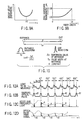
- the electroabsorption optical modulator 2 has light absorption characteristics A shown in FIG. 15 with respect to a negatively applied DC voltage V.
- a DC voltage V is plotted in a linear scale on the abscissa of the light absorption characteristics A, while the light intensity to be output is plotted in a logarithmic (decibel: dB) scale along the ordinate.
- pulses 5 that define a waveform in which minus portions of the sine-wave signal b are compressed and its plus portions are amplified in a linear scale appear at periods Ta of the sine-wave signal b, as shown in FIG. 16B.
- the pulse width Ts of each pulse 5 that forms the optical pulses d output from the light exit surface of the electroabsorption optical modulator 2, i.e., from the optical pulse generation device is expressed by the width of a portion 3 dB below the top of that pulse 5.
- the pulse width Ts of the portion 3 dB below is greatly smaller than the period Ta of the sine-wave signal b.
- the high-duty optical pulses d having the pulse width Ts greatly smaller than the repetition period Ta can be obtained.
- Such requirement is also adamant in an optical sampling pulse generation device that outputs optical sampling pulses used to sample light to be measured, which becomes incident on a light sampling unit in a light sampling waveform measurement apparatus.
- the pulse width Ts of the optical pulses generated by the optical pulse generation device shown in FIG. 14 depends on the period Ta of the sine-wave signal b, i.e., a frequency f A of the sine-wave signal, a pulse width still smaller than the repetition period Ta cannot be obtained.
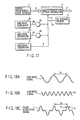
- This optical pulse generation device shown in FIG. 17 comprises a plurality of sine-wave generators 3a and 3b for outputting sine-wave signals b 1 and b 2 (see FIG. 18B; only b 1 is illustrated) having different frequencies with respect to a sine-wave generator 3 for outputting a fundamental sine-wave signal b (see FIG. 18B) having a frequency f A .
- the sine-wave signals b 1 and b 2 are respectively delayed a predetermined amount by delay circuits 6a and 6b, and the delayed signals are added to the fundamental sine-wave signal b, thus obtaining a pulse modulation signal c having sharp peaks, as shown in FIG. 18C.
- the pulse width Ts alone can be shortened without changing the repetition period Ta of optical pulses d output from the light exit surface of this electroabsorption optical modulator 2.
- light a output from a single-wavelength light source 1 is modulated into optical pulses d 1 by a first electroabsorption optical modulator 2a, and is then modulated into optical pulses d 2 by a second electroabsorption optical modulator 2b.
- a rectangular wave signal e 1 (FIG. 20A) output from a rectangular wave generator 7 is applied to the first electroabsorption optical modulator 2a.
- a rectangular signal e 2 (FIG. 20B), which is obtained by delaying the rectangular wave signal e 1 output from the rectangular wave generator 7 a predetermined period of time by a delay circuit 8, is applied to the second electroabsorption optical modulator 2b.
- optical pulses d 2 output from the second electroabsorption optical modulator 2b include pulses 5 having a pulse width Ts corresponding to the overlapping time between the rectangular wave signals e 1 and e 2 , as shown in FIG. 20C.
- optical pulse generation devices shown in FIGS. 17 and 19 still suffer the following problems.
- the delay amounts in delay circuits 6a and 6b must be set with high precision while synchronizing sine-wave generators 3, 3a, and 3b.
- the frequency of the sine-wave signal b is as very high as several GHz to 10 GHz, complicated setting adjustment is required to set the delay amounts with high precision, and the delay amount may vary soon even after they are set with high precision.
- optical pulse generation device shown in FIG. 17 requires a large number of sine-wave generators 3, 3a, and 3b, and delay circuits 6a and 6b, resulting in a complicated circuit arrangement.
- the repetition frequency of the rectangular wave signal e 1 output from the rectangular wave generator 7 is as very high as several GHz to 10 GHz, jitter of around 1 ps is produced at the leading and trailing edges of the rectangular wave.
- the jitter of around 1 ps is not negligible for optical pulses which are required to have a pulse width Ts of 3 to 4 ps.
- the present invention has been made in consideration of the above situation, and has as its object to provide a method and device for generating optical pulses, which can form a sharp peak waveform in a pulse modulation signal to be applied to an electroabsorption optical modulator by a simple circuit arrangement, and can still shorten only the pulse width compared to the repetition period of output optical pulses, and an optical sampling pulse generation apparatus using the device.
- an optical pulse generation method as defined in claim 1 and an optical pulse generation device as defined in claim 2 and further specified in claims 3 to 7.
- Invention above is applied to an optical pulse generation method in which a pulse modulation signal is applied to an electroabsorption optical modulator while continuous, single-wavelength light becomes incident on the electroabsorption optical modulator to modulate the incoming single-wavelength light by the pulse modulation signal, thus outputting the modulated light as optical pulses.
- an electrical signal having a sine waveform is generated, only a waveform equal to or higher than a predetermined DC voltage is extracted from the sine waveform of the electrical signal, a negative DC voltage is added to the electrical signal from which the only the waveform equal to or higher than the predetermined DC voltage is extracted, and the sum signal is then applied to the electroabsorption optical modulator as the pulse modulation signal.
- the optical pulse generation device comprises a single-wavelength light source for outputting continuous, single-wavelength light, an electroabsorption optical modulator for receiving the single-wavelength light output from the single-wavelength light source, modulating the incoming single-wavelength light on the basis of an externally applied pulse modulation signal, and outputting the modulated light as optical pulses, a sine-wave voltage generator for generating an electrical signal having a sine waveform, a nonlinear circuit for extracting only a waveform not less than a predetermined DC voltage from the sine waveform of the electrical signal generated by the sine-wave voltage generator, and a DC voltage source for adding a negative DC voltage to the electrical signal from which only the waveform not less than the predetermined DC voltage is extracted by the nonlinear circuit, and applying the sum signal to the electroabsorption optical modulator as the pulse modulation signal.
- the electrical signal output from the sine-wave voltage generator is rectified and amplified by extracting only the waveform equal to or higher than the predetermined DC voltage from its sine waveform.
- the electrical signal is sliced at an arbitrary signal level including the waveform center of half-wave rectification in a sine-wave signal waveform, and the sliced waveform portion is amplified.
- the pulse modulation signal applied to the electroabsorption optical modulator is the sum signal obtained by extracting only the waveform equal to or higher than the predetermined DC voltage from the sine waveform of the electrical signal, and adding the negative DC voltage to the electrical signal from which only the waveform equal to or higher than the predetermined DC voltage is extracted.
- the nonlinear circuit comprises a half-wave rectification circuit for outputting a half-wave rectified signal of the electrical signal having the sine waveform, which is output from the sine-wave voltage generator, and a voltage amplifier for voltage-amplifying the half-wave rectified signal output from the half-wave rectification circuit.
- the pulse modulation signal applied to the electroabsorption optical modulator is the sum signal obtained by amplifying the half-wave rectified signal by the amplifier, and adding the negative DC voltage to the amplified half-wave rectified signal.
- the voltage value of the pulse modulation signal applied to the electroabsorption optical modulator inevitably has an upper limit value.
- the amplitude value (P - P) of the amplified half-wave rectified signal to be added to the negative DC voltage VA is limited.
- the waveforms of the respective signals when the amplitude value (P - P) of the half-wave rectified signal is equal to that of the sine-wave signal before half-wave rectification are compared.
- the half-wave rectified signal waveform is obtained by extracting only positive portions of the sine-wave signal waveform.
- the half-wave rectified signal waveform is elongated in the vertical direction compared to the sine-wave signal waveform.
- the half-wave rectified signal waveform defines a sharp peak waveform that has larger changes in voltage per unit time than the sine-wave signal waveform.
- the pulse width Ts of modulated optical pulses output from the electroabsorption optical modulator can be greatly smaller than that of conventional optical pulses modulated using the sine-wave signal.
- the repetition period Ta of optical pulses is determined by the frequency f A of the sine-wave signal before half-wave rectification, and is not shortened.
- the pulse width Ts can be further shortened compared to the repetition period Ta of optical pulses output from the electroabsorption optical modulator.
- an electrical signal output from the sine-wave voltage generator is rectified and amplified by extracting only a waveform equal to or higher than a predetermined DC voltage from the sine waveform of that electrical signal. That is, the electrical signal is sliced at an arbitrary signal level including the waveform center of half-wave rectification of claim 2 in a sine-wave signal waveform, and the sliced waveform portion is amplified. Hence, substantially the same effect as in the optical pulse generation method of invention can be obtained.
- the nonlinear circuit comprises a voltage amplifier, an operation point of which can be shifted, and voltage-amplifies the electrical signal having the sine waveform output from the sine-wave voltage generator while the operation point is shifted in a negative direction.
- this optical pulse generation device comprises a single-wavelength light source for outputting continuous, single-wavelength light, an electroabsorption optical modulator for receiving the single-wavelength light output from the single-wavelength light source, modulating the incoming single-wavelength light on the basis of an externally applied pulse modulation signal, and outputting the modulated light as an optical pulse, and a modulation signal generation circuit which comprises a DC voltage source for outputting a negative DC voltage, a sine-wave generation circuit for outputting a sine-wave signal, and a voltage amplifier whose operation point can be shifted, amplifies the sine-wave signal by the voltage amplifier while the operation point is shifted in the negative direction, adds the negative DC voltage to the amplified sine-wave signal, and applies the sum signal to the electroabsorption optical modulator as the pulse modulation signal.
- a modulation signal generation circuit which comprises a DC voltage source for outputting a negative DC voltage, a sine-wave generation circuit for outputting a sine-wave signal, and a voltage amplifier whose operation point can
- the voltage amplifier whose operation point can be shifted is assembled in the optical pulse generation device with this arrangement.
- the sine-wave signal is amplified by that voltage amplifier while the operation point is shifted in the negative direction.
- the amplified sine-wave signal has a waveform obtained by cutting off some minus components.
- the amplified sine-wave signal is approximated to the amplified half-wave rectified signal.
- An optical pulse generation device comprises a single-wavelength light source for outputting continuous, single-wavelength light, a first electroabsorption optical modulator for receiving the single-wavelength light output from the single-wavelength light source, modulating the incoming single-wavelength light on the basis of an externally applied pulse modulation signal, and outputting the modulated light as an optical pulse, a first modulation signal generation circuit which substantially comprises a DC voltage source for outputting a negative DC voltage, a half-wave rectification circuit for outputting a half-wave rectified signal, and a voltage amplifier, amplifies the half-wave rectified signal by the voltage amplifier, adds the negative DC voltage to the amplified half-wave rectified signal, and applies the sum signal to the first electroabsorption optical modulator as the pulse modulation signal, a second electroabsorption optical modulator for receiving optical pulses output from the first electroabsorption optical modulator, modulating the incoming optical pulses on the basis of an externally applied pulse modulation signal, and outputting the modulated optical pulse
- optical pulse generation device with this arrangement, light output from the single-wavelength light source is modulated by the first electroabsorption optical modulator to obtain optical pulses, and these optical pulses are further modulated by the second electroabsorption optical modulator to obtain final optical pulses.
- the first modulation signal generation circuit having the same arrangement as that of the modulation signal generation circuit of claim 2 is connected to the first electroabsorption optical modulator, optical pulses output from the first electroabsorption optical modulator have a small pulse width Ts.
- the pulse modulation signal of the rectangular wave signal that includes optical pulses once every predetermined number of pulses is applied to the second electroabsorption optical modulator, the optical pulses output from the first electroabsorption optical modulator are output once every predetermined number of pulses by decimation.
- the repetition period Ta of pulses is prolonged.
- the pulse width Ta of each pulse of the optical pulses remains the same, the pulse width Ts can be still shortened compared to the pulse repetition period Ta.
- An optical pulse generation device comprises a single-wavelength light source for outputting continuous, single-wavelength light, an electroabsorption optical modulator for receiving the single-wavelength light output from the single-wavelength light source, modulating the incoming single-wavelength light on the basis of an externally applied pulse modulation signal, and outputting the modulated light as an optical pulse, a modulation signal generation circuit which substantially comprises a DC voltage source for outputting a negative DC voltage, a half-wave rectification circuit for outputting a half-wave rectified signal, and a voltage amplifier, amplifies the half-wave rectified signal by the voltage amplifier, adds the negative DC voltage to the amplified half-wave rectified signal, and applies the sum signal to the electroabsorption optical modulator as the pulse modulation signal, and a dispersion decreasing fiber for receiving optical pulses output from the electroabsorption optical modulator at one end, and outputting the incoming optical pulses as final optical pulses from the other end.
- the dispersion decreasing fiber is further connected to the optical pulse generation device according to invention (2) above.
- the dispersion decreasing fiber has characteristics in which the wavelength dispersion of light input from one end decreases with increasing distance if a predetermined wavelength condition and an optical fiber length condition (soliton condition) are satisfied, as is well known.
- the pulse width Ts of optical pulses output from the other end is further shortened.
- An optical sampling pulse generation apparatus has the arrangements of the optical pulse generation devices according to claims 5 and 6 and their features, and also has an arrangement unique to an optical sampling pulse generation apparatus serving as a light sampling waveform measurement apparatus and their features.
- FIG. 1 is a schematic block diagram showing the arrangement of an optical pulse generation device to which an optical pulse generation method according to the first embodiment of the present invention is applied.
- FIG. 1 denote the same parts as those in the conventional optical pulse generation device shown in FIG. 14, and a detailed description thereof will be omitted.
- light a which is a laser beam output from a single-wavelength light source 1 such as a laser beam source or the like, and has a continuous, single wavelength, is launched into the light entrance surface of an electroabsorption optical modulator 2.
- the modulator electrode of this electroabsorption optical modulator 2 receives a pulse modulation signal c 1 , which has a waveform shown in FIG. 2D, from a modulation signal generation circuit 11.
- the electroabsorption optical modulator 2 modulates the light a, which has entered the light entrance surface and has a continuous, single wavelength, by the pulse modulation signal c 1 input to the modulator electrode, and outputs optical pulses d 3 having a waveform shown in FIG. 3B from the light exit surface.
- the modulation signal generation circuit 11 comprises a sine-wave generator 3, half-wave rectifier 12, voltage amplifier 13, and DC voltage source 4, as shown in FIG. 1.
- the sine-wave generator 3 outputs a sine-wave signal b having a frequency f A (several GHz to 10 GHz) (period Ta) shown in, e.g., FIG. 2A, and sends it to the half-wave rectifier 12.
- the half-wave rectifier 12 half-wave rectifies the sine-wave signal b, and outputs it to the next voltage amplifier 13 as a half-wave rectified signal g having a waveform shown in FIG. 2B.
- the voltage amplifier 13 amplifies the half-wave rectified signal g, and outputs an amplified half-wave rectified signal h shown in FIG. 2C.
- the DC voltage source 4 outputs a negative DC voltage Va.
- the negative DC voltage Va is added to the amplified half-wave rectified signal h, and the sum signal is applied to the modulator electrode of the electroabsorption optical modulator 2 as the pulse modulation signal c 1 .
- the amplified half-wave rectified signal h has a sharp peak waveform that has larger changes in voltage per unit time at peak portions of the electrical waveform than the signal obtained by amplifying the sine-wave signal b.
- the amplified half-wave rectified signal h is included on the (+) side of a bias point indicated by the negative DC voltage Va, which is set with respect to modulation characteristics A of the electroabsorption optical modulator 2.
- the electroabsorption optical modulator 2 outputs modulated optical pulses d 3 that repeat waves 5a each having a sharp peak at a period Ta, as shown in FIG. 3B.
- a pulse width Ts in this case corresponds to the sharp peak waveform of the amplified half-wave rectified signal h.
- the duty ratio of the optical pulses d 3 output from the electroabsorption optical modulator 2 can be higher than those obtained by the conventional optical pulse generation device (FIG. 14) which directly uses the sine-wave signal b before half-wave rectification as a pulse modulation signal.
- the pulse width Ts can be further shortened with respect to the repetition period Ta.
- the device of this embodiment is realized by adding a simple circuit arrangement, i.e., the half-wave rectifier 12 and voltage amplifier 13, to the conventional optical pulse generation device shown in FIG. 14, and the arrangement of the overall device can be greatly simplified compared to the conventional optical pulse generation device shown in FIG. 17.
- FIG. 4 is a schematic block diagram showing the arrangement of an optical pulse generation device according to the second embodiment of the present invention.
- FIG. 4 denote the same parts as those in the optical pulse generation device of the first embodiment shown in FIG. 1, and a detailed description thereof will be omitted.
- light a output from a single-wavelength light source 1 is launched into an electroabsorption optical modulator 2, is modulated by a pulse modulation signal c 2 applied by a modulation signal generation circuit 11a, and is output as optical pulses d 4 .
- the modulation signal generation circuit 11a of the second embodiment comprises a sine-wave generator 3, a voltage amplifier 13a whose operation point can be shifted, and a DC voltage source 4, as shown in FIG. 4.
- a sine-wave signal b having a frequency f A (period Ta) output from the sine-wave generator 3 is supplied to the voltage amplifier 13a.
- the voltage amplifier 13a whose operation point can be shifted can arbitrarily set an operation point (bias point) with respect to the input sine-wave signal b upon amplifying the input sine-wave signal b, as shown in FIGS. 5A and 5B.
- the operation point (bias point) is set at zero-volt position of the input sine-wave signal b.
- the amplified sine-wave signal has a normal sine waveform with symmetrical minus and plus components.
- the operation point of the sine-wave signal b is set to shift in the negative direction, as shown in FIG. 5B.
- a sine-wave signal i amplified by this voltage amplifier 13a has a waveform obtained by cutting off some minus components.
- the signal waveform of the amplified sine-wave signal i is approximate to that of the amplified half-wave rectified signal h shown in FIG. 2C in the device of the first embodiment.
- the amplified sine-wave signal i has a sharper peak waveform, as described above.
- a negative DC voltage Va is added to the amplified sine-wave signal i having a sharp peak waveform, and the sum signal is applied to the electroabsorption optical modulator 2 as the pulse modulation signal c 2 .
- the pulse width Ts of the optical pulses d 4 output from the electroabsorption optical modulator 2 can be greatly shortened as in the device of the first embodiment shown in FIG. 1.
- FIG. 6 is a schematic block diagram showing the arrangement of an optical pulse generation device according to the third embodiment of the present invention.
- FIG. 6 denote the same parts as those in the optical pulse generation device of the first embodiment shown in FIG. 1, and a detailed description thereof will be omitted.
- light a output from a single-wavelength light source 1 is modulated by the first electroabsorption optical modulator 2c to obtain optical pulses d 3 , and the optical pulses d 3 are further modulated by the second electroabsorption optical modulator 2d to obtain final optical pulses d 5 .
- a first modulation signal generation circuit 11a having the same arrangement as the modulation signal generation circuit 11 in the device of the first embodiment is connected to the first electroabsorption optical modulator 2c, a first pulse modulation signal c 1 having a sharp peak waveform shown in FIG. 7A is applied to the first electroabsorption optical modulator 2c.
- the optical pulses d 3 output from the first electroabsorption optical modulator 2c have a period Ta and small pulse width Ts, as shown in FIG. 7B.
- a second pulse modulation signal c 3 shown in FIG. 7C is applied from a second modulation signal generation circuit 11c to the second electroabsorption optical modulator 2c.
- the second modulation signal generation circuit 11c comprises a rectangular wave generator 14, sync adjustment circuit 15, and DC voltage source 4a for outputting a negative DC voltage Va.
- the rectangular wave generator 14 outputs a rectangular wave signal j which has a width roughly the same as the period Ta of the sine-wave signal b in the first modulation signal generation circuit 11a, and repeats itself at the same frequency f A .
- the sync adjustment circuit 15 adjusts the output timing of the rectangular wave signal j from the rectangular wave generator 14 so that the respective rectangular waves of the rectangular wave signal j output from the rectangular wave generator 14 include every other optical pulses d 3 output from the first electroabsorption optical modulator 2c, as shown in FIG. 7C.
- the negative DC voltage Va output from the DC voltage source 4a is added to the rectangular wave signal j that has undergone the output timing adjustment, and the sum signal is applied to the second electroabsorption optical modulator 2d as the second pulse modulation signal c 3 .
- the second electroabsorption optical modulator 2d Upon application of the second pulse modulation signal c 3 having the rectangular waveform, the second electroabsorption optical modulator 2d outputs only pulses, which are included in the rectangular waveform of the second pulse modulation signal c 3 , of those which form the optical pulses d 3 input from the first electroabsorption optical modulator 2c.
- the final optical pulses d 5 output from the second electroabsorption optical modulator 2d are optical pulses obtained by decimating every other pulses of the input optical pulses d 3 , as shown in FIG. 7D.
- every other optical pulses are decimated.
- every n-th optical pulses (n is an arbitrary integer) may be output by decimation.
- the pulse repetition period of the optical pulses d 5 is extended to twice (2Ta) the repetition period Ta of the optical pulses d 3 output from the first electroabsorption optical modulator 2c.
- the pulse width Ts of each pulse of the optical pulses d 5 remains the same, the pulse width Ts can be further shortened compared to the repetition period 2Ta of pulses.
- FIG. 8 is a schematic block diagram showing the arrangement of a pulse generation device according to the fourth embodiment of the present invention.
- FIG. 8 denote the same parts as those in the optical pulse generation device of the first embodiment shown in FIG. 1, and a detailed description thereof will be omitted.
- a series circuit of an optical fiber amplifier (EDFA: Erbium Doped Fiber Amplifier) 16 and dispersion decreasing fiber (DDF) 17 is connected to the output terminal for optical pulses of the optical pulse generation device of the first embodiment shown in FIG. 1.
- EDFA Erbium Doped Fiber Amplifier
- DDF dispersion decreasing fiber
- optical pulses d 3 are optically amplified to a predetermined light intensity level by the optical fiber amplifier (EDFA) 16.
- EDFA optical fiber amplifier
- the pulse width Ts of the optical pulses d 3 is further compressed by the dispersion decreasing fiber (DDF) 17, and the optical pulses d 3 are then output as final optical pulses d 6 .
- a modulation signal generation circuit 11 having the same arrangement as that in the device of the first embodiment is connected to the electroabsorption optical modulator 2, a pulse modulation signal c 1 having a sharp peak waveform shown in FIG. 2D is applied to the electroabsorption optical modulator 2.
- the optical pulses d 3 output from the electroabsorption optical modulator 2 have a period Ta and small pulse width Ts.
- DDF dispersion decreasing fiber
- the pulse width of optical pulses which are propagated at high speed in the fiber is broadened due to wavelength dispersion in the propagation process.
- the wavelength dispersion depends on a wavelength ⁇ of light that travels, as shown in FIG. 9A.
- a wavelength ⁇ 0 at which a minimum wavelength dispersion (group delay) is obtained is defined to be zero dispersion wavelength.
- the wavelength ⁇ 0 at which the minimum wavelength dispersion (group delay) is obtained i.e., zero dispersion wavelength, is determined by material dispersion and waveguide dispersion.
- zero dispersion wavelength can be changed in the longitudinal direction of the fiber, as shown in FIG. 9B.
- the dispersion decreasing fiber (DDF) 17 used in the device of this embodiment uses a fiber in which the wavelength dispersion becomes zero dispersion at a fiber length La in the longitudinal direction and dispersion gradually decreases from the input end toward the output end with respect to light having a wavelength of 1.55 ⁇ m that can minimize the loss of a silica-based fiber.
- the Kerr effect that shortens the pulse width of the output pulse waveform requires the power of the input pulse waveform, to be equal to or higher than a prescribed value.
- the amplified optical pulses pass through the dispersion decreasing fiber (DDF) 17 that satisfies the above condition, thus further shortening the pulse width Ts of the-final optical pulses d 6 output from the dispersion decreasing fiber (DDF) 17.
- DDF dispersion decreasing fiber
- the soliton length Ls makes to be shortened.
- the fiber length of the dispersion decreasing fiber (DDF) 17 that extends over ten-odd km required in the conventional manner can be greatly shortened to 4 km order, for example.
- FIG. 11 is a schematic block diagram showing the arrangement of a light sampling waveform measurement apparatus of the fifth embodiment, in which the optical pulse generation device according to one of the above embodiments of the present invention is assembled.
- FIG. 11 denote the same parts as those in the optical pulse generation device of the third embodiment shown in FIG. 6, and a detailed description thereof will be omitted.
- externally input light k to be measured which has a repetition period Tb, as shown in, e.g., FIG. 12A, is input to a clock detector 20 to detect its repetition period Tb, and a clock signal m having the detected repetition period Tb is input to a timing clock generation circuit 21.
- the timing clock generation circuit 21 inputs a sampling clock signal m 1 , which is sequentially delayed a predetermined time ⁇ T from the clock signal m having the period Tb (frequency f), to a half-wave rectifier 12 in a first modulation signal generation circuit 11a in an optical pulse generation device 22.
- the first modulation signal generation circuit 11a applies a first pulse modulation signal c 1 having a sharp peak waveform to a first electroabsorption optical modulator 2c in synchronism with the sampling clock signal m 1 .
- the sampling clock signal m 1 which is output from the timing clock generation circuit 21 and is sequentially delayed the predetermined time ⁇ T at every period Tb, is frequency-divided to 1/N by a frequency divider 23 to obtain a new sampling clock signal m 2 .
- the sampling clock signal m 2 is input to a sync adjustment circuit 15 in a second modulation signal generation circuit 11c in the optical pulse generation device 22.
- the second modulation signal generation circuit 11c applies a second pulse modulation signal c 3 having a rectangular waveform to a second electro-absorption optical modulator 2c in synchronism with the sampling clock signal m 2 .
- optical pulses d 3 are optically amplified by an optical fiber amplifier (EDFA) 16 and then further modulated by the second electroabsorption optical modulator 2c to obtain optical pulses d 5 .
- EDFA optical fiber amplifier
- the optical pulses d 5 are obtained by decimating the optical pulses d 3 output from the first electroabsorption optical modulator 2c to 1/N.
- the optical pulses d 5 are sequentially delayed the predetermined time ⁇ T every time a period (Tb ⁇ N) (frequency f/N) elapses.
- the optical pulses d 5 output from the second electroabsorption optical modulator 2d are input to a dispersion compensated fiber to suppress chirping, and are optically amplified by an optical fiber amplifier (EDFA) 16a again.
- EDFA optical fiber amplifier
- the pulse width of the optical pulses is further shortened by a dispersion decreasing fiber (DDF) 17, and these optical pulses are optically amplified by an optical fiber amplifier (EDFA) 16b.
- the optical pulses are output from the optical pulse generation device 22 and are input to a polarization controller 25.
- the polarization controller 25 controls the polarization direction of the input optical pulses in a 45° direction with respect to the reference direction, as shown in FIG. 11.
- Sampling optical pulses d 7 in the 45° direction output from the polarization controller 25 is launched into one surface of a polarization splitter 27 comprising, e.g., a polarization beam splitter (PBS) or the like in a light sampling unit 26.
- a polarization splitter 27 comprising, e.g., a polarization beam splitter (PBS) or the like in a light sampling unit 26.
- PBS polarization beam splitter
- the sampling optical pulses d 7 become optical pulses which are sequentially delayed the predetermined time ⁇ T every time the period (Tb ⁇ N) (frequency f/N) elapses, as shown in FIG. 12B.
- the light k to be measured is incident on a surface of the polarization splitter 27, that neighbors its one surface.
- a half mirror 27a whose surface has a polarization coat is assembled in the polarization splitter 27.
- the half mirror 27a passes a polarization component in a 90° direction with reference to the reference direction (0° direction) of incoming light.
- a polarization component in the reference direction of the sampling optical pulses d 7 having a plane of polarization in the 45° direction, and that in the 90° direction of the light k to be measured enter a type-2 nonlinear optical material 28a.
- a polarization component in the 90° direction of the sampling optical pulses d 7 and that in the reference direction of the light k to be measured enter another type-2 nonlinear optical material 28b.
- the type-2 nonlinear optical materials 28a and 28b have known physical properties. That is, upon receiving a pair of light components p 1 and p 2 , the polarization directions of which are set in 90° different directions and which respectively have angular frequencies ⁇ S and ⁇ D on one surface, sum frequency light p 3 having a sum angular frequency ( ⁇ S + ⁇ D ) is output from the other surface, as shown in FIG. 13.
- the sampling optical pulses d 7 and light k to be measured are input to the nonlinear optical material 28a, phasing is attained, and the type-2 nonlinear optical material 28a outputs sum frequency light having a sum angular frequency to a next light receiver 29a.
- the sampling optical pulses d 7 and light k to be measured are input to the nonlinear optical material 28b, phasing is attained, and the type-2 nonlinear optical material 28b outputs sum frequency light having a sum angular frequency to a next light receiver 29b.
- calculating added sum frequency light q obtained by adding the sum frequency light components output from the nonlinear optical materials 28a and 28b, a waveform obtained by sampling the waveform of the light k to be measured using the sampling optical pulses d 7 understands to obtain all the time without depending the polarization state of the light k to be measured, as shown in FIG. 12C.
- the light receivers 29a and 29b respectively convert the incoming sum frequency light components into electrical signals n 1 and n 2 , and send them to an adder circuit 30 in the actual system.
- the adder circuit 30 adds the electrical signals n 1 and n 2 , and outputs the sum signal to a next signal processor 31 as an optical pulse train signal n 3 .
- this optical pulse train signal n 3 has a signal waveform in which the signal levels of the individual pulses correspond to the light intensity values of the individual pulses of the added sum frequency light q, as shown in FIG. 12D.
- the signal processor 31 obtains an envelope r that represents a signal waveform obtained by expanding the light k to be measured along the time axis on the basis of the optical pulse train signal n 3 input from the adder circuit 30, and displays on a display 32 the signal waveform of the light k to be measured, which is represented by the envelope r and is expanded along the time axis.
- the pulse width Ts of each pulse in the sampling optical pulses d 7 which are input from the optical pulse generation device 22 to the light sampling unit 26 can be greatly reduced.
- the light signal waveform of the light k to be measured can be sampled using the sampling optical pulses d 7 having a short pulse width Ts, the light signal waveform of the light k to be measured can be sampled at shorter time intervals, thus greatly improving the waveform measurement precision of the light k to be measured.
- the optical pulse generation method and device of the present invention since a sharp peak waveform is formed in a pulse modulation signal to be applied to the electroabsorption optical modulator by a simple circuit arrangement, only the pulse width can be further shortened compared to the repetition period of output optical pulses.
Description
- The present invention relates to an optical pulse generation system and, more particularly, to a method and device for outputting optical pulses having high duty ratio, and an optical sampling pulse generation apparatus using the device.
- Conventionally, as a device for generating high-duty optical pulses which have a repetition frequency ranging from several GHz to 10 GHz used in an optical communication system and a small pulse width, an optical pulse generation device using an electro-absorption optical modulator has been proposed, as shown in FIG. 14 (Jpn. Pat. Appln. KOKAI Publication No. 5-283804).
- In this optical pulse generation device, for example, light a, which is a laser beam output from a single-wavelength light source 1 such as a laser beam source or the like, and has a continuous, single wavelength, becomes incident on the light entrance surface of an electroabsorption optical modulator 2.
- The modulator electrode of this electroabsorption optical modulator 2 receives a pulse modulation signal c, which is obtained by adding a negative DC voltage Va output from a DC voltage source 4 to a sine-wave signal b output from a sine-wave generator 3.
- The electroabsorption optical modulator 2 outputs, from its light exit surface, optical pulses d obtained by modulating the light a, which becomes incident on its light entrance surface and has a continuous, single wavelength, by the pulse modulation signal c input to its modulator electrode.
- The electroabsorption optical modulator 2 has light absorption characteristics A shown in FIG. 15 with respect to a negatively applied DC voltage V.
- A DC voltage V is plotted in a linear scale on the abscissa of the light absorption characteristics A, while the light intensity to be output is plotted in a logarithmic (decibel: dB) scale along the ordinate.
- Hence, when the sine-wave signal b is applied to the modulator electrode of this electroabsorption optical modulator 2 at a bias point that has shifted in the negative direction by the negative DC voltage Va, as shown in FIG. 16A, optical pulses d shown in FIG. 16B are output from the light exit surface of this electroabsorption optical modulator 2.
- More specifically, as the optical pulses d, pulses 5 that define a waveform in which minus portions of the sine-wave signal b are compressed and its plus portions are amplified in a linear scale appear at periods Ta of the sine-wave signal b, as shown in FIG. 16B.
- The pulse width Ts of each pulse 5 that forms the optical pulses d output from the light exit surface of the electroabsorption optical modulator 2, i.e., from the optical pulse generation device is expressed by the width of a portion 3 dB below the top of that pulse 5.
- The pulse width Ts of the portion 3 dB below is greatly smaller than the period Ta of the sine-wave signal b.
- Hence, using the pulse modulation signal c obtained by adding the negative DC voltage Va to the sine-wave signal b, the high-duty optical pulses d having the pulse width Ts greatly smaller than the repetition period Ta can be obtained.
- In recent years, in an optical communication system, the transfer rate of optical signals is increasing, and an optical pulse generation device capable of generating optical pulses d having a pulse width Ts still smaller than the repetition period Ta is required.
- Such requirement is also adamant in an optical sampling pulse generation device that outputs optical sampling pulses used to sample light to be measured, which becomes incident on a light sampling unit in a light sampling waveform measurement apparatus.
- Hence, since the pulse width Ts of the optical pulses generated by the optical pulse generation device shown in FIG. 14 depends on the period Ta of the sine-wave signal b, i.e., a frequency fA of the sine-wave signal, a pulse width still smaller than the repetition period Ta cannot be obtained.
- To combat this problem, an optical pulse generation device shown in FIG. 17 has been proposed (Jpn. Pat. Appln. KOKAI Publication No. 9-133901).
- This optical pulse generation device shown in FIG. 17 comprises a plurality of sine-wave generators 3a and 3b for outputting sine-wave signals b1 and b2 (see FIG. 18B; only b1 is illustrated) having different frequencies with respect to a sine-wave generator 3 for outputting a fundamental sine-wave signal b (see FIG. 18B) having a frequency fA.
- The sine-wave signals b1 and b2 are respectively delayed a predetermined amount by delay circuits 6a and 6b, and the delayed signals are added to the fundamental sine-wave signal b, thus obtaining a pulse modulation signal c having sharp peaks, as shown in FIG. 18C.
- By applying the pulse modulation signal c having sharp peaks to the modulator electrode of an electro-absorption optical modulator 2, the pulse width Ts alone can be shortened without changing the repetition period Ta of optical pulses d output from the light exit surface of this electroabsorption optical modulator 2.
- Furthermore, conventionally, an optical pulse generation device using a rectangular wave signal shown in FIG. 19 has been proposed (Jpn. Pat. Appln. KOKAI Publication No. 5-283804 corresponding to EP-A-0 556 974).
- In the optical pulse generation device shown in FIG. 19, light a output from a single-wavelength light source 1 is modulated into optical pulses d1 by a first electroabsorption optical modulator 2a, and is then modulated into optical pulses d2 by a second electroabsorption optical modulator 2b.
- A rectangular wave signal e1 (FIG. 20A) output from a rectangular wave generator 7 is applied to the first electroabsorption optical modulator 2a.
- On the other hand, a rectangular signal e2 (FIG. 20B), which is obtained by delaying the rectangular wave signal e1 output from the rectangular wave generator 7 a predetermined period of time by a delay circuit 8, is applied to the second electroabsorption optical modulator 2b.
- As a result, optical pulses d2 output from the second electroabsorption optical modulator 2b include pulses 5 having a pulse width Ts corresponding to the overlapping time between the rectangular wave signals e1 and e2, as shown in FIG. 20C.
- Hence, when a short overlapping time between the rectangular wave signals e1 and e2 is set by adjusting the delay time of the delay circuit 8, as shown in FIGS. 20A, 20B, and 20C, only the pulse width Ts can be shortened without changing the repetition period Ta of the output optical pulses d2.
- However, the optical pulse generation devices shown in FIGS. 17 and 19 still suffer the following problems.
- In the optical pulse generation device shown in FIG. 17, in order to obtain the pulse modulation signal c having sharp peaks shown in FIG. 18C, the delay amounts in delay circuits 6a and 6b must be set with high precision while synchronizing sine-wave generators 3, 3a, and 3b.
- In this case, since the frequency of the sine-wave signal b is as very high as several GHz to 10 GHz, complicated setting adjustment is required to set the delay amounts with high precision, and the delay amount may vary soon even after they are set with high precision.
- Furthermore, the optical pulse generation device shown in FIG. 17 requires a large number of sine-wave generators 3, 3a, and 3b, and delay circuits 6a and 6b, resulting in a complicated circuit arrangement.
- In the optical pulse generation device shown in FIG. 19, since the repetition frequency of the rectangular wave signal e1 output from the rectangular wave generator 7 is as very high as several GHz to 10 GHz, jitter of around 1 ps is produced at the leading and trailing edges of the rectangular wave.
- As a consequence, jitter of around 1 ps is produced in the optical pulses d2 output from this optical pulse generation device.
- The jitter of around 1 ps is not negligible for optical pulses which are required to have a pulse width Ts of 3 to 4 ps.
- Consequently, in this pulse generation device, decreasing the pulse width Ts of the output optical pulses d2 by setting a short overlapping time between the rectangular wave signals e1 and e2 is limited.
- The present invention has been made in consideration of the above situation, and has as its object to provide a method and device for generating optical pulses, which can form a sharp peak waveform in a pulse modulation signal to be applied to an electroabsorption optical modulator by a simple circuit arrangement, and can still shorten only the pulse width compared to the repetition period of output optical pulses, and an optical sampling pulse generation apparatus using the device.
- In order to achieve the above object, according to the present invention, there is provided an optical pulse generation method as defined in claim 1, and an optical pulse generation device as defined in claim 2 and further specified in claims 3 to 7.
- Invention above is applied to an optical pulse generation method in which a pulse modulation signal is applied to an electroabsorption optical modulator while continuous, single-wavelength light becomes incident on the electroabsorption optical modulator to modulate the incoming single-wavelength light by the pulse modulation signal, thus outputting the modulated light as optical pulses.
- In order to achieve the above object, according to the invention , an electrical signal having a sine waveform is generated, only a waveform equal to or higher than a predetermined DC voltage is extracted from the sine waveform of the electrical signal, a negative DC voltage is added to the electrical signal from which the only the waveform equal to or higher than the predetermined DC voltage is extracted, and the sum signal is then applied to the electroabsorption optical modulator as the pulse modulation signal.
- The optical pulse generation device according to the invention above comprises a single-wavelength light source for outputting continuous, single-wavelength light, an electroabsorption optical modulator for receiving the single-wavelength light output from the single-wavelength light source, modulating the incoming single-wavelength light on the basis of an externally applied pulse modulation signal, and outputting the modulated light as optical pulses, a sine-wave voltage generator for generating an electrical signal having a sine waveform, a nonlinear circuit for extracting only a waveform not less than a predetermined DC voltage from the sine waveform of the electrical signal generated by the sine-wave voltage generator, and a DC voltage source for adding a negative DC voltage to the electrical signal from which only the waveform not less than the predetermined DC voltage is extracted by the nonlinear circuit, and applying the sum signal to the electroabsorption optical modulator as the pulse modulation signal.
- In the optical pulse generation device with this arrangement, the electrical signal output from the sine-wave voltage generator is rectified and amplified by extracting only the waveform equal to or higher than the predetermined DC voltage from its sine waveform.
- That is, the electrical signal is sliced at an arbitrary signal level including the waveform center of half-wave rectification in a sine-wave signal waveform, and the sliced waveform portion is amplified.
- Hence, substantially the same effect as in the optical pulse generation method of the invention can be obtained.
- In the optical pulse generation method and device with the above arrangement, the pulse modulation signal applied to the electroabsorption optical modulator is the sum signal obtained by extracting only the waveform equal to or higher than the predetermined DC voltage from the sine waveform of the electrical signal, and adding the negative DC voltage to the electrical signal from which only the waveform equal to or higher than the predetermined DC voltage is extracted.
- In the optical pulse generation device according to claim 3, the nonlinear circuit comprises a half-wave rectification circuit for outputting a half-wave rectified signal of the electrical signal having the sine waveform, which is output from the sine-wave voltage generator, and a voltage amplifier for voltage-amplifying the half-wave rectified signal output from the half-wave rectification circuit.
- In the optical pulse generation device with this arrangement, the pulse modulation signal applied to the electroabsorption optical modulator is the sum signal obtained by amplifying the half-wave rectified signal by the amplifier, and adding the negative DC voltage to the amplified half-wave rectified signal.
- In this case, the voltage value of the pulse modulation signal applied to the electroabsorption optical modulator inevitably has an upper limit value.
- Since the bias point in light absorption characteristics A shown in FIG. 15 is also limited, the amplitude value (P - P) of the amplified half-wave rectified signal to be added to the negative DC voltage VA is limited.
- The waveforms of the respective signals when the amplitude value (P - P) of the half-wave rectified signal is equal to that of the sine-wave signal before half-wave rectification are compared.
- Of these signals, the half-wave rectified signal waveform is obtained by extracting only positive portions of the sine-wave signal waveform.
- Hence, when the amplitude values (P - P) are equal to each other, the half-wave rectified signal waveform is elongated in the vertical direction compared to the sine-wave signal waveform.
- As a result, the half-wave rectified signal waveform defines a sharp peak waveform that has larger changes in voltage per unit time than the sine-wave signal waveform.
- Hence, the pulse width Ts of modulated optical pulses output from the electroabsorption optical modulator can be greatly smaller than that of conventional optical pulses modulated using the sine-wave signal.
- Note that the repetition period Ta of optical pulses is determined by the frequency fA of the sine-wave signal before half-wave rectification, and is not shortened.
- Therefore, only the pulse width Ts can be further shortened compared to the repetition period Ta of optical pulses output from the electroabsorption optical modulator.
- In the optical pulse generation device with this arrangement, an electrical signal output from the sine-wave voltage generator is rectified and amplified by extracting only a waveform equal to or higher than a predetermined DC voltage from the sine waveform of that electrical signal. That is, the electrical signal is sliced at an arbitrary signal level including the waveform center of half-wave rectification of claim 2 in a sine-wave signal waveform, and the sliced waveform portion is amplified. Hence, substantially the same effect as in the optical pulse generation method of invention can be obtained.
- In the optical pulse generation device according to claim 4, the nonlinear circuit comprises a voltage amplifier, an operation point of which can be shifted, and voltage-amplifies the electrical signal having the sine waveform output from the sine-wave voltage generator while the operation point is shifted in a negative direction.
- That is, this optical pulse generation device comprises a single-wavelength light source for outputting continuous, single-wavelength light, an electroabsorption optical modulator for receiving the single-wavelength light output from the single-wavelength light source, modulating the incoming single-wavelength light on the basis of an externally applied pulse modulation signal, and outputting the modulated light as an optical pulse, and a modulation signal generation circuit which comprises a DC voltage source for outputting a negative DC voltage, a sine-wave generation circuit for outputting a sine-wave signal, and a voltage amplifier whose operation point can be shifted, amplifies the sine-wave signal by the voltage amplifier while the operation point is shifted in the negative direction, adds the negative DC voltage to the amplified sine-wave signal, and applies the sum signal to the electroabsorption optical modulator as the pulse modulation signal.
- The voltage amplifier whose operation point can be shifted is assembled in the optical pulse generation device with this arrangement. The sine-wave signal is amplified by that voltage amplifier while the operation point is shifted in the negative direction.
- Hence, the amplified sine-wave signal has a waveform obtained by cutting off some minus components.
- As a result, the amplified sine-wave signal is approximated to the amplified half-wave rectified signal.
- At this time, when the amplitude value (P - P) of the amplified signal is constant, since the amplified sine-wave signal has a sharp peak waveform having a larger change in voltage per unit time, as described above, nearly the same effect as in the above inventions can be obtained.
- An optical pulse generation device according to claim 5 comprises a single-wavelength light source for outputting continuous, single-wavelength light, a first electroabsorption optical modulator for receiving the single-wavelength light output from the single-wavelength light source, modulating the incoming single-wavelength light on the basis of an externally applied pulse modulation signal, and outputting the modulated light as an optical pulse, a first modulation signal generation circuit which substantially comprises a DC voltage source for outputting a negative DC voltage, a half-wave rectification circuit for outputting a half-wave rectified signal, and a voltage amplifier, amplifies the half-wave rectified signal by the voltage amplifier, adds the negative DC voltage to the amplified half-wave rectified signal, and applies the sum signal to the first electroabsorption optical modulator as the pulse modulation signal, a second electroabsorption optical modulator for receiving optical pulses output from the first electroabsorption optical modulator, modulating the incoming optical pulses on the basis of an externally applied pulse modulation signal, and outputting the modulated optical pulses as final optical pulses, and a second modulation signal generation circuit which comprises a DC voltage source for outputting a negative DC voltage, a rectangular wave signal generation circuit for outputting a rectangular wave signal, and a sync adjustment circuit, synchronously adjusts the rectangular wave signal output from the rectangular wave signal generation circuit using the sync adjustment circuit so that individual rectangular waves of the rectangular wave signal include optical pulses once every predetermined number of pulses, adds the negative DC voltage to the adjusted rectangular wave signal, and applies the sum signal to the second electroabsorption optical modulator as the pulse modulation signal.
- In the optical pulse generation device with this arrangement, light output from the single-wavelength light source is modulated by the first electroabsorption optical modulator to obtain optical pulses, and these optical pulses are further modulated by the second electroabsorption optical modulator to obtain final optical pulses.
- Since the first modulation signal generation circuit having the same arrangement as that of the modulation signal generation circuit of claim 2 is connected to the first electroabsorption optical modulator, optical pulses output from the first electroabsorption optical modulator have a small pulse width Ts.
- Since the pulse modulation signal of the rectangular wave signal, that includes optical pulses once every predetermined number of pulses is applied to the second electroabsorption optical modulator, the optical pulses output from the first electroabsorption optical modulator are output once every predetermined number of pulses by decimation.
- As a consequence, the repetition period Ta of pulses is prolonged. However, since the pulse width Ta of each pulse of the optical pulses remains the same, the pulse width Ts can be still shortened compared to the pulse repetition period Ta.
- An optical pulse generation device according to claim 6 comprises a single-wavelength light source for outputting continuous, single-wavelength light, an electroabsorption optical modulator for receiving the single-wavelength light output from the single-wavelength light source, modulating the incoming single-wavelength light on the basis of an externally applied pulse modulation signal, and outputting the modulated light as an optical pulse, a modulation signal generation circuit which substantially comprises a DC voltage source for outputting a negative DC voltage, a half-wave rectification circuit for outputting a half-wave rectified signal, and a voltage amplifier, amplifies the half-wave rectified signal by the voltage amplifier, adds the negative DC voltage to the amplified half-wave rectified signal, and applies the sum signal to the electroabsorption optical modulator as the pulse modulation signal, and a dispersion decreasing fiber for receiving optical pulses output from the electroabsorption optical modulator at one end, and outputting the incoming optical pulses as final optical pulses from the other end.
- In the optical pulse generation device with this arrangement, the dispersion decreasing fiber is further connected to the optical pulse generation device according to invention (2) above.
- The dispersion decreasing fiber has characteristics in which the wavelength dispersion of light input from one end decreases with increasing distance if a predetermined wavelength condition and an optical fiber length condition (soliton condition) are satisfied, as is well known.
- As a result, the pulse width Ts of optical pulses output from the other end is further shortened.
- An optical sampling pulse generation apparatus according to claim 7 has the arrangements of the optical pulse generation devices according to claims 5 and 6 and their features, and also has an arrangement unique to an optical sampling pulse generation apparatus serving as a light sampling waveform measurement apparatus and their features.
- This summary of the invention does not necessarily describe all necessary features so that the invention may also be a sub-combination of these described features.
- The invention can be more fully under stood from the following detailed description when taken in conjunction with the accompanying drawings, in which:
- FIG. 1 is a schematic block diagram showing the arrangement of an optical pulse generation device according to the first embodiment to which an optical pulse generation method of the present invention is applied;
- FIGS. 2A to 2D are signal waveform charts of the respective units for explaining the operation of a modulation signal generation circuit of the optical pulse generation device according to the first embodiment;
- FIGS. 3A and 3B are respectively a graph for explaining modulation of an electroabsorption optical modulator in the optical pulse generator according to the first embodiment, and a waveform chart of output optical pulses;
- FIG. 4 is a schematic block diagram showing the arrangement of an optical pulse generation device according to the second embodiment of the present invention;
- FIGS. 5A and 5B are graphs for explaining amplification of a voltage amplifier whose operation point can be shifted, in the optical pulse generation device according to the second embodiment;
- FIG. 6 is a schematic block diagram showing the arrangement of an optical pulse generation device according to the third embodiment of the present invention;
- FIGS. 7A to 7D are waveform charts of the respective signals for explaining the operation of the pulse generation device according to the third embodiment;
- FIG. 8 is a schematic block diagram showing the arrangement of an optical pulse generation device according to the fourth embodiment of the present invention;
- FIGS. 9A and 9B are graphs showing the wavelength dispersion characteristics of a dispersion decreasing fiber used in the optical pulse generation device according to the fourth embodiment;
- FIG. 10 is a view for explaining the wavelength dispersion characteristics of the dispersion decreasing fiber used in the optical pulse generation device according to the fourth embodiment;
- FIG. 11 is a schematic block diagram showing the arrangement of a light sampling waveform measurement apparatus of the fifth embodiment in which an optical pulse generation device according to the present invention is assembled;
- FIGS. 12A to 12D are signal waveform charts of the respective units for explaining the operation principle of the light sampling waveform measurement apparatus shown in FIG. 11;
- FIG. 13 is a perspective view for explaining the optical characteristics of a nonlinear optical material used in the light sampling waveform measurement apparatus shown in FIG. 11;
- FIG. 14 is a schematic block diagram showing the arrangement of a conventional optical pulse generation device;
- FIG. 15 is a graph showing the light absorption characteristics of an electroabsorption optical modulator;
- FIGS. 16A and 16B are respectively a graph showing modulation of the electroabsorption optical modulator in the conventional optical pulse generation device shown in FIG. 14, and a waveform chart of output optical pulses;
- FIG. 17 is a schematic block diagram showing the arrangement of another conventional optical pulse generation device;
- FIGS. 18A, 18B, and 18C are waveform charts of a sine-wave signal and modulated signal in the conventional optical pulse generation device shown in FIG. 17;
- FIG. 19 is a schematic block diagram showing the arrangement of still another conventional optical pulse generation device;
- FIGS. 20A, 20B, and 20C are waveform charts of a modulated signal and output optical pulses in the conventional optical pulse generation device shown in FIG. 19; and
- FIG. 21 is a waveform chart for explaining jitter produced in the modulated signal in the conventional optical pulse generation device shown in FIG. 19.
-
- Reference will now be made in detail to the presently preferred embodiments of the invention as illustrated in the accompanying drawings, in which like reference numerals designate like or corresponding parts.
- The preferred embodiments of the present invention will now be described with reference to the accompanying drawings.
- FIG. 1 is a schematic block diagram showing the arrangement of an optical pulse generation device to which an optical pulse generation method according to the first embodiment of the present invention is applied.
- The same reference numerals in FIG. 1 denote the same parts as those in the conventional optical pulse generation device shown in FIG. 14, and a detailed description thereof will be omitted.
- More specifically, as shown in FIG. 1, light a, which is a laser beam output from a single-wavelength light source 1 such as a laser beam source or the like, and has a continuous, single wavelength, is launched into the light entrance surface of an electroabsorption optical modulator 2.
- The modulator electrode of this electroabsorption optical modulator 2 receives a pulse modulation signal c1, which has a waveform shown in FIG. 2D, from a modulation signal generation circuit 11.
- The electroabsorption optical modulator 2 modulates the light a, which has entered the light entrance surface and has a continuous, single wavelength, by the pulse modulation signal c1 input to the modulator electrode, and outputs optical pulses d3 having a waveform shown in FIG. 3B from the light exit surface.
- The modulation signal generation circuit 11 comprises a sine-wave generator 3, half-wave rectifier 12, voltage amplifier 13, and DC voltage source 4, as shown in FIG. 1.
- The sine-wave generator 3 outputs a sine-wave signal b having a frequency fA (several GHz to 10 GHz) (period Ta) shown in, e.g., FIG. 2A, and sends it to the half-wave rectifier 12.
- The half-wave rectifier 12 half-wave rectifies the sine-wave signal b, and outputs it to the next voltage amplifier 13 as a half-wave rectified signal g having a waveform shown in FIG. 2B.
- The voltage amplifier 13 amplifies the half-wave rectified signal g, and outputs an amplified half-wave rectified signal h shown in FIG. 2C.
- The DC voltage source 4 outputs a negative DC voltage Va.
- The negative DC voltage Va is added to the amplified half-wave rectified signal h, and the sum signal is applied to the modulator electrode of the electroabsorption optical modulator 2 as the pulse modulation signal c1.
- In the optical pulse generation device with this arrangement, as described above, the amplified half-wave rectified signal h has a sharp peak waveform that has larger changes in voltage per unit time at peak portions of the electrical waveform than the signal obtained by amplifying the sine-wave signal b.
- As shown in FIG. 3A, the amplified half-wave rectified signal h is included on the (+) side of a bias point indicated by the negative DC voltage Va, which is set with respect to modulation characteristics A of the electroabsorption optical modulator 2.
- Hence, the electroabsorption optical modulator 2 outputs modulated optical pulses d3 that repeat waves 5a each having a sharp peak at a period Ta, as shown in FIG. 3B.
- A pulse width Ts in this case corresponds to the sharp peak waveform of the amplified half-wave rectified signal h.
- Therefore, the duty ratio of the optical pulses d3 output from the electroabsorption optical modulator 2 can be higher than those obtained by the conventional optical pulse generation device (FIG. 14) which directly uses the sine-wave signal b before half-wave rectification as a pulse modulation signal.
- That is, the pulse width Ts can be further shortened with respect to the repetition period Ta.
- Furthermore, the device of this embodiment is realized by adding a simple circuit arrangement, i.e., the half-wave rectifier 12 and voltage amplifier 13, to the conventional optical pulse generation device shown in FIG. 14, and the arrangement of the overall device can be greatly simplified compared to the conventional optical pulse generation device shown in FIG. 17.
- FIG. 4 is a schematic block diagram showing the arrangement of an optical pulse generation device according to the second embodiment of the present invention.
- The same reference numerals in FIG. 4 denote the same parts as those in the optical pulse generation device of the first embodiment shown in FIG. 1, and a detailed description thereof will be omitted.
- More specifically, as shown in FIG. 4, light a output from a single-wavelength light source 1 is launched into an electroabsorption optical modulator 2, is modulated by a pulse modulation signal c2 applied by a modulation signal generation circuit 11a, and is output as optical pulses d4.
- The modulation signal generation circuit 11a of the second embodiment comprises a sine-wave generator 3, a voltage amplifier 13a whose operation point can be shifted, and a DC voltage source 4, as shown in FIG. 4.
- A sine-wave signal b having a frequency fA (period Ta) output from the sine-wave generator 3 is supplied to the voltage amplifier 13a.
- The voltage amplifier 13a whose operation point can be shifted can arbitrarily set an operation point (bias point) with respect to the input sine-wave signal b upon amplifying the input sine-wave signal b, as shown in FIGS. 5A and 5B.
- In FIG. 5A, the operation point (bias point) is set at zero-volt position of the input sine-wave signal b.
- In this case, the amplified sine-wave signal has a normal sine waveform with symmetrical minus and plus components.
- However, in the device of the second embodiment, the operation point of the sine-wave signal b is set to shift in the negative direction, as shown in FIG. 5B.
- Therefore, a sine-wave signal i amplified by this voltage amplifier 13a has a waveform obtained by cutting off some minus components.
- Accordingly, the signal waveform of the amplified sine-wave signal i is approximate to that of the amplified half-wave rectified signal h shown in FIG. 2C in the device of the first embodiment.
- when the amplitude value (P - P) of this amplified signal is constant, the amplified sine-wave signal i has a sharper peak waveform, as described above.
- A negative DC voltage Va is added to the amplified sine-wave signal i having a sharp peak waveform, and the sum signal is applied to the electroabsorption optical modulator 2 as the pulse modulation signal c2.
- Hence, the pulse width Ts of the optical pulses d4 output from the electroabsorption optical modulator 2 can be greatly shortened as in the device of the first embodiment shown in FIG. 1.
- FIG. 6 is a schematic block diagram showing the arrangement of an optical pulse generation device according to the third embodiment of the present invention.
- The same reference numerals in FIG. 6 denote the same parts as those in the optical pulse generation device of the first embodiment shown in FIG. 1, and a detailed description thereof will be omitted.
- In the optical pulse generation device of this embodiment, two electroabsorption optical modulators 2c and 2d having the same arrangement are assembled.
- More specifically, light a output from a single-wavelength light source 1 is modulated by the first electroabsorption optical modulator 2c to obtain optical pulses d3, and the optical pulses d3 are further modulated by the second electroabsorption optical modulator 2d to obtain final optical pulses d5.
- Since a first modulation signal generation circuit 11a having the same arrangement as the modulation signal generation circuit 11 in the device of the first embodiment is connected to the first electroabsorption optical modulator 2c, a first pulse modulation signal c1 having a sharp peak waveform shown in FIG. 7A is applied to the first electroabsorption optical modulator 2c.
- Hence, the optical pulses d3 output from the first electroabsorption optical modulator 2c have a period Ta and small pulse width Ts, as shown in FIG. 7B.
- A second pulse modulation signal c3 shown in FIG. 7C is applied from a second modulation signal generation circuit 11c to the second electroabsorption optical modulator 2c.
- As shown in FIG. 6, the second modulation signal generation circuit 11c comprises a rectangular wave generator 14, sync adjustment circuit 15, and DC voltage source 4a for outputting a negative DC voltage Va.
- The rectangular wave generator 14 outputs a rectangular wave signal j which has a width roughly the same as the period Ta of the sine-wave signal b in the first modulation signal generation circuit 11a, and repeats itself at the same frequency fA.
- The sync adjustment circuit 15 adjusts the output timing of the rectangular wave signal j from the rectangular wave generator 14 so that the respective rectangular waves of the rectangular wave signal j output from the rectangular wave generator 14 include every other optical pulses d3 output from the first electroabsorption optical modulator 2c, as shown in FIG. 7C.
- The negative DC voltage Va output from the DC voltage source 4a is added to the rectangular wave signal j that has undergone the output timing adjustment, and the sum signal is applied to the second electroabsorption optical modulator 2d as the second pulse modulation signal c3.
- Upon application of the second pulse modulation signal c3 having the rectangular waveform, the second electroabsorption optical modulator 2d outputs only pulses, which are included in the rectangular waveform of the second pulse modulation signal c3, of those which form the optical pulses d3 input from the first electroabsorption optical modulator 2c.
- Hence, the final optical pulses d5 output from the second electroabsorption optical modulator 2d are optical pulses obtained by decimating every other pulses of the input optical pulses d3, as shown in FIG. 7D.
- In the device of this embodiment, every other optical pulses are decimated. However, every n-th optical pulses (n is an arbitrary integer) may be output by decimation.
- As a result, the pulse repetition period of the optical pulses d5 is extended to twice (2Ta) the repetition period Ta of the optical pulses d3 output from the first electroabsorption optical modulator 2c.
- However, since the pulse width Ts of each pulse of the optical pulses d5 remains the same, the pulse width Ts can be further shortened compared to the repetition period 2Ta of pulses.
- That is, a higher duty ratio can be realized.
- FIG. 8 is a schematic block diagram showing the arrangement of a pulse generation device according to the fourth embodiment of the present invention.
- The same reference numerals in FIG. 8 denote the same parts as those in the optical pulse generation device of the first embodiment shown in FIG. 1, and a detailed description thereof will be omitted.
- In the optical pulse generation device of this embodiment, a series circuit of an optical fiber amplifier (EDFA: Erbium Doped Fiber Amplifier) 16 and dispersion decreasing fiber (DDF) 17 is connected to the output terminal for optical pulses of the optical pulse generation device of the first embodiment shown in FIG. 1.
- More specifically, as shown in FIG. 8, light an output from a single-wavelength light source 1 is modulated by an electroabsorption optical modulator 2 to obtain optical pulses d3, and the optical pulses d3 are optically amplified to a predetermined light intensity level by the optical fiber amplifier (EDFA) 16. After that, the pulse width Ts of the optical pulses d3 is further compressed by the dispersion decreasing fiber (DDF) 17, and the optical pulses d3 are then output as final optical pulses d6.
- Since a modulation signal generation circuit 11 having the same arrangement as that in the device of the first embodiment is connected to the electroabsorption optical modulator 2, a pulse modulation signal c1 having a sharp peak waveform shown in FIG. 2D is applied to the electroabsorption optical modulator 2.
- Hence, the optical pulses d3 output from the electroabsorption optical modulator 2 have a period Ta and small pulse width Ts.
- Specific features of the dispersion decreasing fiber (DDF) 17 will be explained below.
- The pulse width of optical pulses which are propagated at high speed in the fiber is broadened due to wavelength dispersion in the propagation process.
- The wavelength dispersion (group delay) depends on a wavelength λ of light that travels, as shown in FIG. 9A.
- A wavelength λ0 at which a minimum wavelength dispersion (group delay) is obtained is defined to be zero dispersion wavelength.
- The wavelength λ0 at which the minimum wavelength dispersion (group delay) is obtained, i.e., zero dispersion wavelength, is determined by material dispersion and waveguide dispersion.
- Hence, by changing the waveguide dispersion of the optical fiber, zero dispersion wavelength can be changed in the longitudinal direction of the fiber, as shown in FIG. 9B.
- The dispersion decreasing fiber (DDF) 17 used in the device of this embodiment uses a fiber in which the wavelength dispersion becomes zero dispersion at a fiber length La in the longitudinal direction and dispersion gradually decreases from the input end toward the output end with respect to light having a wavelength of 1.55 µm that can minimize the loss of a silica-based fiber.
- On the other hand, as shown in FIG. 10, when a fiber length Ls satisfies a soliton condition including a wavelength condition of zero dispersion wavelength, the Kerr effect that shortens the pulse width of the output pulse waveform from this fiber is produced when the input pulse waveform to this fiber has large power.
- Note that the Kerr effect that shortens the pulse width of the output pulse waveform requires the power of the input pulse waveform, to be equal to or higher than a prescribed value.
- Hence, in the device of the fourth embodiment, after the optical pulses d3 output from the electro-absorption optical modulator 2 are optically amplified to a prescribed level by the optical fiber amplifier (EDFA) 16, the amplified optical pulses pass through the dispersion decreasing fiber (DDF) 17 that satisfies the above condition, thus further shortening the pulse width Ts of the-final optical pulses d6 output from the dispersion decreasing fiber (DDF) 17.
- Furthermore, as shown in FIG. 10, the relationship among a soliton length that satisfies the soliton condition of the fiber, a dispersion value β2 that characterizes the input pulse waveform to the fiber which satisfies the silicon condition, and a pulse width T0 is given by:
- As can be seen from equation (1), in order to shorten the soliton length Ls as the fiber length of the dispersion decreasing fiber (DDF) 17, it is more effective to shorten the pulse width T0 that influences the soliton length by its square.
- In the device of the fourth embodiment, since the pulse width Ts of the optical pulses d3 output from the electroabsorption optical modulator 2 has been shortened in comparison with a conventional manner, the soliton length Ls makes to be shortened.
- Hence, the fiber length of the dispersion decreasing fiber (DDF) 17 that extends over ten-odd km required in the conventional manner can be greatly shortened to 4 km order, for example.
- FIG. 11 is a schematic block diagram showing the arrangement of a light sampling waveform measurement apparatus of the fifth embodiment, in which the optical pulse generation device according to one of the above embodiments of the present invention is assembled.
- The same reference numeral in FIG. 11 denote the same parts as those in the optical pulse generation device of the third embodiment shown in FIG. 6, and a detailed description thereof will be omitted.
- More specifically, as shown in FIG. 11, externally input light k to be measured, which has a repetition period Tb, as shown in, e.g., FIG. 12A, is input to a clock detector 20 to detect its repetition period Tb, and a clock signal m having the detected repetition period Tb is input to a timing clock generation circuit 21.
- The timing clock generation circuit 21 inputs a sampling clock signal m1, which is sequentially delayed a predetermined time ΔT from the clock signal m having the period Tb (frequency f), to a half-wave rectifier 12 in a first modulation signal generation circuit 11a in an optical pulse generation device 22.
- Hence, the first modulation signal generation circuit 11a applies a first pulse modulation signal c1 having a sharp peak waveform to a first electroabsorption optical modulator 2c in synchronism with the sampling clock signal m1.
- The sampling clock signal m1, which is output from the timing clock generation circuit 21 and is sequentially delayed the predetermined time ΔT at every period Tb, is frequency-divided to 1/N by a frequency divider 23 to obtain a new sampling clock signal m2. The sampling clock signal m2 is input to a sync adjustment circuit 15 in a second modulation signal generation circuit 11c in the optical pulse generation device 22.
- Hence, the second modulation signal generation circuit 11c applies a second pulse modulation signal c3 having a rectangular waveform to a second electro-absorption optical modulator 2c in synchronism with the sampling clock signal m2.
- Then, light a output from a single-wavelength light source 1 is modulated by the first electroabsorption optical modulator 2c to obtain optical pulses d3, and the optical pulses d3 are optically amplified by an optical fiber amplifier (EDFA) 16 and then further modulated by the second electroabsorption optical modulator 2c to obtain optical pulses d5.
- Hence, the optical pulses d5 are obtained by decimating the optical pulses d3 output from the first electroabsorption optical modulator 2c to 1/N.
- More specifically, the optical pulses d5 are sequentially delayed the predetermined time ΔT every time a period (Tb × N) (frequency f/N) elapses.
- The optical pulses d5 output from the second electroabsorption optical modulator 2d are input to a dispersion compensated fiber to suppress chirping, and are optically amplified by an optical fiber amplifier (EDFA) 16a again.
- After that, the pulse width of the optical pulses is further shortened by a dispersion decreasing fiber (DDF) 17, and these optical pulses are optically amplified by an optical fiber amplifier (EDFA) 16b. The optical pulses are output from the optical pulse generation device 22 and are input to a polarization controller 25.
- The polarization controller 25 controls the polarization direction of the input optical pulses in a 45° direction with respect to the reference direction, as shown in FIG. 11.
- Sampling optical pulses d7 in the 45° direction output from the polarization controller 25 is launched into one surface of a polarization splitter 27 comprising, e.g., a polarization beam splitter (PBS) or the like in a light sampling unit 26.
- More specifically, the sampling optical pulses d7 become optical pulses which are sequentially delayed the predetermined time ΔT every time the period (Tb × N) (frequency f/N) elapses, as shown in FIG. 12B.
- Note that the light k to be measured is incident on a surface of the polarization splitter 27, that neighbors its one surface.
- A half mirror 27a whose surface has a polarization coat is assembled in the polarization splitter 27.
- The half mirror 27a passes a polarization component in a 90° direction with reference to the reference direction (0° direction) of incoming light.
- Hence, a polarization component in the reference direction of the sampling optical pulses d7 having a plane of polarization in the 45° direction, and that in the 90° direction of the light k to be measured enter a type-2 nonlinear optical material 28a.
- On the other hand, a polarization component in the 90° direction of the sampling optical pulses d7 and that in the reference direction of the light k to be measured enter another type-2 nonlinear optical material 28b.
- The type-2 nonlinear optical materials 28a and 28b have known physical properties. That is, upon receiving a pair of light components p1 and p2, the polarization directions of which are set in 90° different directions and which respectively have angular frequencies ωS and ωD on one surface, sum frequency light p3 having a sum angular frequency (ωS + ωD) is output from the other surface, as shown in FIG. 13.
- Therefore, since the sampling optical pulses d7 and light k to be measured, the planes of polarization of which are set in 90° different directions, are input to the nonlinear optical material 28a, phasing is attained, and the type-2 nonlinear optical material 28a outputs sum frequency light having a sum angular frequency to a next light receiver 29a.
- Likewise, since the sampling optical pulses d7 and light k to be measured, the planes of polarization of which are set in 90° different directions, are input to the nonlinear optical material 28b, phasing is attained, and the type-2 nonlinear optical material 28b outputs sum frequency light having a sum angular frequency to a next light receiver 29b.
- Hence, calculating added sum frequency light q obtained by adding the sum frequency light components output from the nonlinear optical materials 28a and 28b, a waveform obtained by sampling the waveform of the light k to be measured using the sampling optical pulses d7, understands to obtain all the time without depending the polarization state of the light k to be measured, as shown in FIG. 12C.
- The light receivers 29a and 29b respectively convert the incoming sum frequency light components into electrical signals n1 and n2, and send them to an adder circuit 30 in the actual system.
- The adder circuit 30 adds the electrical signals n1 and n2, and outputs the sum signal to a next signal processor 31 as an optical pulse train signal n3.
- Hence, this optical pulse train signal n3 has a signal waveform in which the signal levels of the individual pulses correspond to the light intensity values of the individual pulses of the added sum frequency light q, as shown in FIG. 12D.
- The signal processor 31 obtains an envelope r that represents a signal waveform obtained by expanding the light k to be measured along the time axis on the basis of the optical pulse train signal n3 input from the adder circuit 30, and displays on a display 32 the signal waveform of the light k to be measured, which is represented by the envelope r and is expanded along the time axis.
- In the light sampling waveform measurement apparatus with the above arrangement, the pulse width Ts of each pulse in the sampling optical pulses d7 which are input from the optical pulse generation device 22 to the light sampling unit 26 can be greatly reduced.
- Therefore, since the light signal waveform of the light k to be measured can be sampled using the sampling optical pulses d7 having a short pulse width Ts, the light signal waveform of the light k to be measured can be sampled at shorter time intervals, thus greatly improving the waveform measurement precision of the light k to be measured.
- As described above, in the optical pulse generation method and device of the present invention, since a sharp peak waveform is formed in a pulse modulation signal to be applied to the electroabsorption optical modulator by a simple circuit arrangement, only the pulse width can be further shortened compared to the repetition period of output optical pulses.
Claims (7)
- An optical pulse generation method in which a pulse modulation signal is applied to an electro-absorption optical modulator (2) while continuous, single-wavelength light is launched into the electroabsorption optical modulator (2) so as to modulate the incoming single-wavelength light by the pulse modulation signal and to output the modulated light as optical pulses, comprising the steps of:characterized bygenerating an electrical signal having a sine waveform;
extracting only a waveform not less than a predetermined DC voltage from the sine waveform of the electrical signal; and
adding a negative DC voltage to the extracted waveform, and applying the sum signal to the electroabsorption optical modulator (2) as the pulse modulation signal. - An optical pulse generation device comprising:a single-wavelength light source (1) for outputting continuous, single-wavelength light;a first electroabsorption optical modulator (2) for receiving the single-wavelength light output from said single-wavelength light source (1), modulating the incoming single-wavelength light according to an externally applied pulse modulation signal, and outputting the modulated light as optical pulses;a first modulation signal generation circuit (11a) comprising:a) a sine-wave voltage generator (3) for generating an electrical signal having a sine waveform;b) a nonlinear circuit (12, 13, 13a) for extracting only a waveform not less than a predetermined DC voltage from the sine waveform of the electrical signal generated by said sine-wave voltage generator (3); andc) a DC voltage source (4) for adding a negative DC voltage to the electrical signal waveform extracted by said nonlinear circuit (12, 13, 13a), and applying the sum signal to said electroabsorption optical modulator (2) as the pulse modulation signal.
- A device according to claim 2, wherein said nonlinear circuit comprises:a half-wave rectification circuit (12) for outputting a half-wave rectified signal of the electrical signal having the sine waveform, which is output from said sine-wave voltage generator (3); anda voltage amplifier (13) for voltage-amplifying the half-wave rectified signal output from said half-wave rectification circuit (12).
- A device according to claim 2, wherein said nonlinear circuit comprises a voltage amplifier (13a), an operation point of which can be shifted, to voltage-amplify the electrical signal having the sine waveform output from said sine-wave voltage generator (3) while the operation point is shifted in a negative direction.
- A device according to claim 2, characterized by further comprising:said second modulation signal generation circuit (11c) synchronously adjusting the rectangular wave signal output from said rectangular wave signal generation circuit (14) by said sync adjustment circuit (15) to make individual rectangular waves of the rectangular wave signals include optical pulses once every predetermined number of pulses, adding the negative DC voltage output from said further DC voltage source (4a) to the adjusted rectangular wave signal, and applying the sum signal to said second electroabsorption optical modulator as the pulse modulation signal.a second electroabsorption optical modulator (2d) for receiving the optical pulses output from said first electroabsorption optical modulator (2c), modulating the incoming pulses according to an externally applied pulse modulation signal and outputting the modulated optical pulses as final optical pulses; anda second modulation signal generation circuit (11c) comprisinga) a further DC voltage source (4a) for outputting a negative DC voltage,b) a rectangular wave signal generation circuit (14) for outputting a rectangular wave signal, andc) a sync adjustment circuit (15),
- A device according to claim 2, further comprising:a dispersion decreasing fiber (17) for receiving the optical pulses output from said electroabsorption optical modulator (2) at one end, and outputting the incoming optical pulses as final optical pulses from the other end.
- A device according to claim 5, for outputting optical sampling pulses used to sample light to be measured, which enters an optical sampling unit in an optical sampling waveform measurement apparatus, further comprising:a dispersion decreasing fiber (17) for receiving the optical pulses output from said second electroabsorption optical modulator (2d) at one end, and outputting the incoming optical pulses as final optical pulses from the other end;a timing clock generation circuit (20, 21) for supplying a first sampling clock signal which is delayed a predetermined time from a clock signal based on a repetition period of the light to be measured to said nonlinear circuit of said first modulation signal generation circuit (11a) as the electrical signal having the sine waveform; anda frequency divider (23) for supplying a second sampling clock signal which is obtained by frequency-dividing the first sampling clock signal from said timing clock generation circuit (20, 21) at a predetermined ratio to said sync adjustment circuit (15) of said second modulation signal generation circuit (11c).
Applications Claiming Priority (2)
| Application Number | Priority Date | Filing Date | Title |
|---|---|---|---|
| JP36685898A JP3810570B2 (en) | 1998-12-24 | 1998-12-24 | Optical pulse generation method and apparatus |
| JP36685898 | 1998-12-24 |
Publications (2)
| Publication Number | Publication Date |
|---|---|
| EP1016891A1 EP1016891A1 (en) | 2000-07-05 |
| EP1016891B1 true EP1016891B1 (en) | 2004-07-21 |
Family
ID=18487862
Family Applications (1)
| Application Number | Title | Priority Date | Filing Date |
|---|---|---|---|
| EP99124481A Expired - Lifetime EP1016891B1 (en) | 1998-12-24 | 1999-12-08 | Optical pulse generation system for generating optical pulses having high duty ratio |
Country Status (4)
| Country | Link |
|---|---|
| US (1) | US6483624B1 (en) |
| EP (1) | EP1016891B1 (en) |
| JP (1) | JP3810570B2 (en) |
| DE (1) | DE69918791T2 (en) |
Families Citing this family (24)
| Publication number | Priority date | Publication date | Assignee | Title |
|---|---|---|---|---|
| US6671237B1 (en) * | 2000-02-29 | 2003-12-30 | Imation Corp. | Method and apparatus for driving an electro-optic modulator assembly |
| JP4426077B2 (en) * | 2000-08-10 | 2010-03-03 | アンリツ株式会社 | Pulse generator |
| FR2824152B1 (en) * | 2001-04-27 | 2004-01-30 | Cit Alcatel | OPTICAL TRANSMITTER COMPRISING A MODULATOR COMPOSED OF A PLURALITY OF MODULATION ELEMENTS |
| SE523350C2 (en) * | 2001-08-01 | 2004-04-13 | Optillion Ab | Modulator transmitter for fiber optic communication at high speeds |
| US20030121028A1 (en) * | 2001-12-22 | 2003-06-26 | Michael Coury | Quantum computing integrated development environment |
| GB0200939D0 (en) * | 2002-01-16 | 2002-03-06 | Denselight Semiconductors Pte | An electroabsorption modulator |
| WO2004056016A1 (en) * | 2002-12-16 | 2004-07-01 | Fujitsu Limited | Drive circuit and drive method for optical modulator |
| US7707255B2 (en) | 2003-07-01 | 2010-04-27 | Microsoft Corporation | Automatic grouping of electronic mail |
| US8255828B2 (en) | 2004-08-16 | 2012-08-28 | Microsoft Corporation | Command user interface for displaying selectable software functionality controls |
| US8146016B2 (en) | 2004-08-16 | 2012-03-27 | Microsoft Corporation | User interface for displaying a gallery of formatting options applicable to a selected object |
| US7703036B2 (en) | 2004-08-16 | 2010-04-20 | Microsoft Corporation | User interface for displaying selectable software functionality controls that are relevant to a selected object |
| US8627222B2 (en) | 2005-09-12 | 2014-01-07 | Microsoft Corporation | Expanded search and find user interface |
| US9727989B2 (en) | 2006-06-01 | 2017-08-08 | Microsoft Technology Licensing, Llc | Modifying and formatting a chart using pictorially provided chart elements |
| US7345610B2 (en) * | 2006-06-12 | 2008-03-18 | Wisconsin Alumni Research Foundation | High speed digital-to-analog converter |
| JP2008209214A (en) * | 2007-02-26 | 2008-09-11 | Advantest Corp | Light sampling apparatus |
| EP1971036A1 (en) * | 2007-03-14 | 2008-09-17 | Dtu | A method and a device for detection of a first signal superimposed on a second signal |
| US8484578B2 (en) | 2007-06-29 | 2013-07-09 | Microsoft Corporation | Communication between a document editor in-space user interface and a document editor out-space user interface |
| US8762880B2 (en) | 2007-06-29 | 2014-06-24 | Microsoft Corporation | Exposing non-authoring features through document status information in an out-space user interface |
| EP2241039A1 (en) * | 2008-01-28 | 2010-10-20 | Technion Research and Development Foundation, Ltd. | Optical under-sampling and reconstruction of sparse multiband signals |
| US9665850B2 (en) | 2008-06-20 | 2017-05-30 | Microsoft Technology Licensing, Llc | Synchronized conversation-centric message list and message reading pane |
| US20120155567A1 (en) * | 2010-12-20 | 2012-06-21 | Samsung Electro-Mechanics Co., Ltd. | Data transmission apparatus and transmission method thereof |
| JP6400235B1 (en) * | 2017-06-21 | 2018-10-03 | 三菱電機株式会社 | Optical transmission device and optical transmission method |
| US11368227B2 (en) * | 2019-12-03 | 2022-06-21 | Macom Technology Solutions Holdings, Inc. | Reference optical signal generator |
| US11784856B2 (en) | 2021-01-22 | 2023-10-10 | Macom Technology Solutions Holdings, Inc. | Area efficient high-speed sequence generator and error checker |
Family Cites Families (8)
| Publication number | Priority date | Publication date | Assignee | Title |
|---|---|---|---|---|
| EP0430230B1 (en) * | 1989-11-30 | 1995-03-15 | Nec Corporation | Optical transmitting apparatus |
| JP2764845B2 (en) * | 1992-02-03 | 1998-06-11 | 国際電信電話株式会社 | Optical pulse generator |
| US5394260A (en) | 1992-02-03 | 1995-02-28 | Kokusai Denshin Denwa Kabushiki Kaisha | Optical pulse generator |
| JP2819080B2 (en) | 1993-03-25 | 1998-10-30 | 国際電信電話株式会社 | Optical pulse generator |
| JP3345214B2 (en) * | 1995-03-20 | 2002-11-18 | ケイディーディーアイ株式会社 | Short light pulse modulation method and apparatus |
| JP3406441B2 (en) | 1995-11-08 | 2003-05-12 | Kddi株式会社 | Optical pulse generator |
| DE19603403A1 (en) * | 1996-01-31 | 1997-08-07 | Sel Alcatel Ag | Optical transmission system in which disturbing optical interferences are reduced in the control center |
| US5974209A (en) * | 1998-04-30 | 1999-10-26 | Cho; Pak Shing | System comprising an electroabsorption modulator and an optical discriminator |
-
1998
- 1998-12-24 JP JP36685898A patent/JP3810570B2/en not_active Expired - Fee Related
-
1999
- 1999-12-06 US US09/455,562 patent/US6483624B1/en not_active Expired - Fee Related
- 1999-12-08 EP EP99124481A patent/EP1016891B1/en not_active Expired - Lifetime
- 1999-12-08 DE DE69918791T patent/DE69918791T2/en not_active Expired - Lifetime
Also Published As
| Publication number | Publication date |
|---|---|
| DE69918791T2 (en) | 2005-07-21 |
| JP2000187190A (en) | 2000-07-04 |
| DE69918791D1 (en) | 2004-08-26 |
| JP3810570B2 (en) | 2006-08-16 |
| EP1016891A1 (en) | 2000-07-05 |
| US6483624B1 (en) | 2002-11-19 |
Similar Documents
| Publication | Publication Date | Title |
|---|---|---|
| EP1016891B1 (en) | Optical pulse generation system for generating optical pulses having high duty ratio | |
| US7428096B2 (en) | Optical pulse compressor, optical function generator, optical pulse compression method, and optical function generation method | |
| EP0720312B1 (en) | Soliton data transmission using non-soliton transmitter | |
| JP2005124192A (en) | Method and system for synchronizing operation characteristic of variable wavelength device to wavelength of local oscillator signal | |
| US20020149824A1 (en) | Synchronization of an optical pulse stream with an electrical signal | |
| US7142570B2 (en) | Apparatus and method for generating optical carrier for microwave and millimeterwave photonics system | |
| JPH08265265A (en) | Short light pulse modulation method and device therefor | |
| US7006230B2 (en) | Interferometric method and apparatus for the characterization of optical pulses | |
| US5870211A (en) | Error rate measurement system for high speed optical pulse signals | |
| US6856723B1 (en) | Group velocity dispersion measuring device and group velocity dispersion measuring method | |
| CA2143051C (en) | Method for the generation of ultra-short optical pulses | |
| US4411520A (en) | Light dispersion measuring apparatus | |
| US6462860B1 (en) | Method and apparatus of detection of pulse position modulated optical signals | |
| EP0817409A2 (en) | Method and device for the generation of ultrashort optical pulses | |
| US7171082B2 (en) | Method and apparatus for optical top-hat pulse generation | |
| Bosworth et al. | Electro-optically derived millimeter-wave sources with phase and amplitude control | |
| JP2972885B1 (en) | Optical fiber dispersion measurement method | |
| EP0102537A1 (en) | A method in the signal processing of a received train of pulses, and a receiver for carrying out the process | |
| US6839159B2 (en) | Demultiplexer for optical time-division multiplexed signals | |
| JP3286151B2 (en) | Optical sampling device | |
| JP3031589B2 (en) | Optical frequency stabilizer | |
| KR100204843B1 (en) | Apparatus for measuring pulse-width and pulse-shape for ultra short optical pulse train | |
| JPH1062570A (en) | Method and apparatus for measuring time lag | |
| JPH0795009B2 (en) | Optical fiber transmission characteristic measuring device | |
| JP2007060307A (en) | Optical signal generator |
Legal Events
| Date | Code | Title | Description |
|---|---|---|---|
| PUAI | Public reference made under article 153(3) epc to a published international application that has entered the european phase |
Free format text: ORIGINAL CODE: 0009012 |
|
| 17P | Request for examination filed |
Effective date: 20000126 |
|
| AK | Designated contracting states |
Kind code of ref document: A1 Designated state(s): DE FR GB |
|
| AX | Request for extension of the european patent |
Free format text: AL;LT;LV;MK;RO;SI |
|
| AKX | Designation fees paid |
Free format text: DE FR GB |
|
| 17Q | First examination report despatched |
Effective date: 20020107 |
|
| GRAP | Despatch of communication of intention to grant a patent |
Free format text: ORIGINAL CODE: EPIDOSNIGR1 |
|
| GRAS | Grant fee paid |
Free format text: ORIGINAL CODE: EPIDOSNIGR3 |
|
| GRAA | (expected) grant |
Free format text: ORIGINAL CODE: 0009210 |
|
| AK | Designated contracting states |
Kind code of ref document: B1 Designated state(s): DE FR GB |
|
| REG | Reference to a national code |
Ref country code: GB Ref legal event code: FG4D |
|
| REF | Corresponds to: |
Ref document number: 69918791 Country of ref document: DE Date of ref document: 20040826 Kind code of ref document: P |
|
| ET | Fr: translation filed | ||
| PLBE | No opposition filed within time limit |
Free format text: ORIGINAL CODE: 0009261 |
|
| STAA | Information on the status of an ep patent application or granted ep patent |
Free format text: STATUS: NO OPPOSITION FILED WITHIN TIME LIMIT |
|
| 26N | No opposition filed |
Effective date: 20050422 |
|
| PGFP | Annual fee paid to national office [announced via postgrant information from national office to epo] |
Ref country code: DE Payment date: 20131204 Year of fee payment: 15 Ref country code: GB Payment date: 20131204 Year of fee payment: 15 |
|
| PGFP | Annual fee paid to national office [announced via postgrant information from national office to epo] |
Ref country code: FR Payment date: 20131209 Year of fee payment: 15 |
|
| REG | Reference to a national code |
Ref country code: DE Ref legal event code: R231 Ref document number: 69918791 Country of ref document: DE |
|
| PG25 | Lapsed in a contracting state [announced via postgrant information from national office to epo] |
Ref country code: DE Free format text: LAPSE BECAUSE OF THE APPLICANT RENOUNCES Effective date: 20150618 |
|
| GBPC | Gb: european patent ceased through non-payment of renewal fee |
Effective date: 20141208 |
|
| REG | Reference to a national code |
Ref country code: FR Ref legal event code: ST Effective date: 20150831 |
|
| PG25 | Lapsed in a contracting state [announced via postgrant information from national office to epo] |
Ref country code: GB Free format text: LAPSE BECAUSE OF NON-PAYMENT OF DUE FEES Effective date: 20141208 |
|
| PG25 | Lapsed in a contracting state [announced via postgrant information from national office to epo] |
Ref country code: FR Free format text: LAPSE BECAUSE OF NON-PAYMENT OF DUE FEES Effective date: 20141231 |