EP1016201B1 - Regelbarer spannungswandler mit ladungspumpe - Google Patents
Regelbarer spannungswandler mit ladungspumpe Download PDFInfo
- Publication number
- EP1016201B1 EP1016201B1 EP98921168A EP98921168A EP1016201B1 EP 1016201 B1 EP1016201 B1 EP 1016201B1 EP 98921168 A EP98921168 A EP 98921168A EP 98921168 A EP98921168 A EP 98921168A EP 1016201 B1 EP1016201 B1 EP 1016201B1
- Authority
- EP
- European Patent Office
- Prior art keywords
- voltage
- output
- charging
- charge pump
- power supply
- Prior art date
- Legal status (The legal status is an assumption and is not a legal conclusion. Google has not performed a legal analysis and makes no representation as to the accuracy of the status listed.)
- Expired - Lifetime
Links
- 239000003990 capacitor Substances 0.000 claims description 51
- 230000001419 dependent effect Effects 0.000 claims description 10
- 230000001105 regulatory effect Effects 0.000 claims description 2
- 238000009795 derivation Methods 0.000 claims 4
- 230000008878 coupling Effects 0.000 claims 1
- 238000010168 coupling process Methods 0.000 claims 1
- 238000005859 coupling reaction Methods 0.000 claims 1
- 231100001261 hazardous Toxicity 0.000 description 10
- 238000004886 process control Methods 0.000 description 7
- 230000001276 controlling effect Effects 0.000 description 6
- 238000004146 energy storage Methods 0.000 description 5
- 239000002360 explosive Substances 0.000 description 5
- 238000000034 method Methods 0.000 description 5
- 230000004888 barrier function Effects 0.000 description 4
- 238000010586 diagram Methods 0.000 description 4
- 239000004973 liquid crystal related substance Substances 0.000 description 3
- 238000013459 approach Methods 0.000 description 2
- 230000008901 benefit Effects 0.000 description 2
- 230000006735 deficit Effects 0.000 description 2
- 230000000694 effects Effects 0.000 description 2
- 230000006870 function Effects 0.000 description 2
- 230000008569 process Effects 0.000 description 2
- 102100034871 C-C motif chemokine 8 Human genes 0.000 description 1
- 101000946794 Homo sapiens C-C motif chemokine 8 Proteins 0.000 description 1
- 230000009286 beneficial effect Effects 0.000 description 1
- 238000005538 encapsulation Methods 0.000 description 1
- 230000007613 environmental effect Effects 0.000 description 1
- 238000001914 filtration Methods 0.000 description 1
- 238000002955 isolation Methods 0.000 description 1
- 239000000463 material Substances 0.000 description 1
- 230000007246 mechanism Effects 0.000 description 1
- 230000008450 motivation Effects 0.000 description 1
- 230000001681 protective effect Effects 0.000 description 1
- 230000004044 response Effects 0.000 description 1
- 230000000007 visual effect Effects 0.000 description 1
Images

Classifications
-
- H—ELECTRICITY
- H02—GENERATION; CONVERSION OR DISTRIBUTION OF ELECTRIC POWER
- H02M—APPARATUS FOR CONVERSION BETWEEN AC AND AC, BETWEEN AC AND DC, OR BETWEEN DC AND DC, AND FOR USE WITH MAINS OR SIMILAR POWER SUPPLY SYSTEMS; CONVERSION OF DC OR AC INPUT POWER INTO SURGE OUTPUT POWER; CONTROL OR REGULATION THEREOF
- H02M3/00—Conversion of DC power input into DC power output
- H02M3/02—Conversion of DC power input into DC power output without intermediate conversion into AC
- H02M3/04—Conversion of DC power input into DC power output without intermediate conversion into AC by static converters
- H02M3/06—Conversion of DC power input into DC power output without intermediate conversion into AC by static converters using resistors or capacitors, e.g. potential divider
- H02M3/07—Conversion of DC power input into DC power output without intermediate conversion into AC by static converters using resistors or capacitors, e.g. potential divider using capacitors charged and discharged alternately by semiconductor devices with control electrode, e.g. charge pumps
-
- H—ELECTRICITY
- H05—ELECTRIC TECHNIQUES NOT OTHERWISE PROVIDED FOR
- H05B—ELECTRIC HEATING; ELECTRIC LIGHT SOURCES NOT OTHERWISE PROVIDED FOR; CIRCUIT ARRANGEMENTS FOR ELECTRIC LIGHT SOURCES, IN GENERAL
- H05B45/00—Circuit arrangements for operating light-emitting diodes [LED]
- H05B45/10—Controlling the intensity of the light
- H05B45/14—Controlling the intensity of the light using electrical feedback from LEDs or from LED modules
-
- H—ELECTRICITY
- H05—ELECTRIC TECHNIQUES NOT OTHERWISE PROVIDED FOR
- H05B—ELECTRIC HEATING; ELECTRIC LIGHT SOURCES NOT OTHERWISE PROVIDED FOR; CIRCUIT ARRANGEMENTS FOR ELECTRIC LIGHT SOURCES, IN GENERAL
- H05B45/00—Circuit arrangements for operating light-emitting diodes [LED]
- H05B45/30—Driver circuits
- H05B45/37—Converter circuits
-
- H—ELECTRICITY
- H05—ELECTRIC TECHNIQUES NOT OTHERWISE PROVIDED FOR
- H05B—ELECTRIC HEATING; ELECTRIC LIGHT SOURCES NOT OTHERWISE PROVIDED FOR; CIRCUIT ARRANGEMENTS FOR ELECTRIC LIGHT SOURCES, IN GENERAL
- H05B45/00—Circuit arrangements for operating light-emitting diodes [LED]
- H05B45/30—Driver circuits
- H05B45/395—Linear regulators
Definitions
- This invention relates to an adjustable output charge pump and more particularly to a power supply and contrast adjust circuit for an intrinsically safe backlit liquid crystal display utilizing an adjustable output charge pump.
- Hazardous areas are those sections of a process control plant that have the possibility of an explosive environment.
- process control instrumentation In order to be safely utilized in a hazardous area, process control instrumentation must utilize protective measures to prevent the ignition of materials in the explosive environment. This can be achieved by various methods, including encapsulation, pressurization, and the use of flameproof containment. These methods work by preventing the flammable atmosphere from contacting the device where hot surfaces or sparks might cause ignition.
- Intrinsic safety is another method of protection in which the atmosphere is allowed to come in contact with the equipment only because the equipment has been designed in a way that it is incapable of causing ignition in the atmosphere, even in the presence of faults occurring within or applied to the equipment.
- Intrinsic safety requirements are met by limiting the amount of energy in a circuit such that sparks and heat cannot be generated at levels sufficient to ignite the atmosphere.
- the amount of energy in an intrinsically safe circuit is limited both in terms of instantaneous energy and in terms of stored energy.
- the instantaneous energy is limited by "barrier" circuits that are located in a flameproof enclosure or a safe area. Typically most of the circuitry comprising a piece of process control instrumentation is maintained in a safe area or in a flameproof enclosure located in a hazardous area. Every connection between the circuit within the flameproof enclosure and the IS circuit is through a barrier circuit that limits the maximum current and voltage available to the IS circuit.
- the components used in barrier circuits are relatively large and relatively expensive thus product cost and package size increases as the number of connections to an IS circuit increases.
- the stored energy in the IS circuit is limited by minimizing the size of energy storage devices, e.g. capacitors and inductors, in the IS circuit.
- field-mount display It is desirable for instrumentation used in process plants to provide a local visual readout of data (referred to herein as "field-mount display”). Not only are field-mount displays valued by users of process control instrumentation but backlit displays are preferable to aid reading the displays in low light conditions. Intrinsic safety requirements present difficult implementation issues regarding field-mount displays, especially backlit displays. A field-mount display can be encapsulated within a transparent explosion-proof enclosure but this is an extremely expensive solution that is not realistic for most applications. The intrinsic safety requirements limit the amount of power that can be supplied to the field-mount display. Also, a backlit Liquid Crystal Display (“LCD display”) requires three power supplies. One supply to power the digital circuitry, a second supply for the display contrast and a third supply for backlighting. Existing LCD displays in the process control industry are therefore relatively small (one or two line displays) and are not backlit.
- LCD display liquid crystal Display
- LCD display backlit Liquid Crystal Display
- the above described problems and others are solved and an advance in the art is achieved by the power supply and contrast adjust system of the present invention.
- the system of the present invention provides an intrinsically safe, backlit LCD display that receives all of its power over only two connections from a flameproof enclosure. Two additional connections provide a signal to the display. All three power supplies for the IS circuit are achieved through careful utilization of the single supplied IS voltage and the use of a charge pump with a unique architecture.
- a single intrinsically safe voltage (IS_PWR) is supplied over two connections (between IS_PWR+ and IS_PWR-) from a safe area or flameproof enclosure to the IS circuit.
- the display requires three supply voltages for proper operation.
- V CC (+5V) is the supply used to power the digital circuitry of the LCD display.
- V EE is a variable negative supply used for contrast control of the LCD display.
- V bl is the supply for the backlight. Low voltage backlighting is provided by a floating array of light-emitting diodes thus the common mode voltage of V bl is irrelevant. In the system of the present invention, all three of these supply voltages are derived from IS_PWR.
- V CC is derived using a negative regulator to, in effect, use the "top" 5 volts of IS_PWR as the 5V V CC supply.
- This provides the V CC voltage to the display but also has the advantage that the overhead voltage of the regulator is not wasted.
- the overhead voltage of the negative regulator is summed to the output of a charge pump to provide the V EE supply.
- the backlight is satisfied by the raw IS_PWR supply voltage as the backlight circuit consists of a floating array of diodes and the common mode voltage is irrelevant.
- a charge pump is used to convert IS_PWR to a variable, negative V EE to control the LCD contrast.
- Existing contrast control circuits use a fixed negative supply voltage with an adjustable secondary pass element, e.g. an op-amp and a transistor, to vary the amplitude of the voltage supplied to the display to accomplish contrast adjustment.
- the pass element requires voltage overhead that in combination with the required display capacitance violates intrinsic safety requirements with respect to energy storage elements.
- the voltage stored on the charging capacitor of the charge pump is controlled such that the output of the charge pump is at the desired voltage level without the need for any further control elements.
- a single stage of charge pump includes two capacitors. The charging capacitor is charged to the input voltage and then is discharged into the filter capacitor. The charge pump generates an output voltage that is dependent upon the voltage stored across the charging capacitor.
- a transistor is placed in series with the charging capacitor. The impedance of the transistor is controlled to "steal" voltage away from the charging capacitor.
- the output of the charge pump is directly controlled by controlling the impedance of the transistor with a control loop to produce the desired charge pump output.
- the output of the charge pump is summed with the overhead voltage of the negative regulator to produce a V EE that is variable from about -4V to about -12V.
- the charge pump of the present invention is operated at a relatively high frequency in order to minimize the size of capacitors in the charge pump. This further enhances the intrinsic safety characteristics of the system of the present invention.
- the present invention utilizes a single supply (IS_PWR) of about 9 Volts to derive V CC (+5V), V EE (-4V to -12V) and V bl (+9V).
- IS_PWR single supply
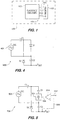
- FIG. 1 is a schematic diagram of a piece of process control instrumentation 101 within a hazardous environment 100.
- Instrumentation 101 is comprised of flameproof enclosure 102 which is connected to intrinsically safe circuit ("IS circuit") 103 through connections 104.
- IS circuit intrinsically safe circuit
- An intrinsically safe circuit is a circuit in which any spark or any thermal effect produced by the circuit is not capable of causing ignition of a given explosive atmosphere such as hazardous environment 100.
- Various standards organizations around the World have defined what a hazardous environment is and set standards for the design of instrumentation to be used in such areas.
- European Standard EN 50020 (“Electrical apparatus for potentially explosive atmospheres - Intrinsic safety 'i'”) is an example of such a standard.
- Standards such as European Standard EN 50020 define the instantaneous power (in terms of current and voltage levels) of all signals over connections 104 to IS circuit 103. These standards also define the allowable amount of stored energy in IS circuit 103.
- misapplications of IS circuit 103, or countable and non-countable faults as prescribed in such standards, that might occur in IS circuit 103 or circuits contained within flameproof enclosure 102, must not result in enough energy available at IS circuit 103 to cause the ignition of a certain explosive atmosphere such as exists in hazardous environment 100.
- FIG. 2 depicts the interface between IS circuit 103 and flameproof enclosure 102 in more detail.
- Elements 200-205 comprise a power supply which is external to IS circuit 103 and which provides an intrinsically safe source of power over lines IS_PWR+ and IS_PWR- to IS circuit 103.
- Transformer 201 provides the fundamental galvanic isolation for IS_PWR supplied to IS circuit 103.
- Fuse 200 protects transformer 201 from heat rise and provides an upper limit to the current on the secondary of transformer 201.
- Rectifier 202 rectifies the AC voltage on the secondary of transformer 201.
- Regulator 203 takes the rectified AC voltage from rectifier 202 as input and outputs a regulated DC voltage. In a preferred embodiment of the present invention the output of voltage regulator 203 is 11V.
- Intrinsic Safety ("I.S.) barrier 205 includes zener diodes arranged to limit the output voltage of I.S. Barrier 205 over IS_PWR+ and IS_PWR-.
- the charge pump circuit of the present invention is used to provide power for an LCD display.
- IS_PWR is manipulated, as described below, to provide the necessary and various power supplies.
- Signals are sent to the LCD display and received from the LCD display via lines IS_TX and IS_RX, respectively. These lines are isolated from the remaining circuitry (not shown) within flameproof enclosure 102 by opto-couplers 206 and 207 and interfaces 208 and 209.
- the selection and operation of elements 200-209 are not pertinent to the present invention. They are described here only for purposes of providing the context for the origination of IS_PWR whose use is described in the remainder of the specification.
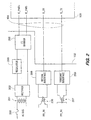
- FIG. 3 depicts a block diagram of a power supply and contrast control circuit 300 within IS circuit 103.
- a single fixed, intrinsically safe power source, IS_PWR is provided over lines IS_PWR+ and IS_PWR-.
- IS_PWR is generated externally to IS circuit 103.
- IS_TX and IS_RX the transmit and receive signals communicated from and to, respectively, the circuit contained within flameproof enclosure 102 are received over lines 301 by microprocessor 302.
- Microprocessor 302 processes these signals to produce human-readable output on LCD 303.
- the operation of microprocessor 302 to produce output on LCD 303 is well-known to those skilled in the art and does not form part of the present invention.
- LCD 303 requires three different power supplies for proper operation. All three supplies, V CC , V EE and V bl , are generated, as described below, from IS_PWR.
- IS_PWR is designed for nominal operation at 150 milliamps (mA) at 9 volts to optimally satisfy both the intrinsic safety requirements of European Standard EN 50020 as well as the operational requirements of circuit 300 and LCD 303.
- European Standard EN 50020 specifies the maximum allowable short circuit current for each value of open circuit voltage, e.g. IS_PWR, V CC , V EE and V bl , implicitly limiting the instantaneous amount of energy available in the hazardous area.
- the values of various protection devices are determined in such a way as to deliver the maximum amount of power at the desired operational output voltage and output current while simultaneously remaining below the energy limits dictated by European Standard EN 50020.
- V CC is the supply for the digital circuitry of circuit 300. In the preferred embodiment of the present invention, V CC is about 5V and must supply about 30mA maximum current.
- V EE is the voltage applied to LCD 303 to control the contrast of LCD 303. In the preferred embodiment of the present invention, V EE is variable from -4V to about -12V and must supply about 20mA maximum current.
- V bl is the voltage applied to LCD 303 to power backlight array 311 of LCD 303. Typically backlighting for an LCD display is accomplished with an array 311 of diodes which emit light when an appropriate voltage is applied across the array 311. In the preferred embodiment of the present invention V bl is about 8.5V and must supply about 100mA maximum current. Thus, in the preferred embodiment of the present invention, IS_PWR must supply about 150mA at about 9V.
- Negative voltage regulator 304 is coupled between IS_PWR+and IS_PWR-. Voltage regulator 304 effectively derives ground 5V below IS_PWR+ to provide a V CC of 5V at the V CC input to LCD 303. There are other topologies by which one can derive a ground but using negative voltage regulator 304 has the advantage of not wasting the voltage overhead of the regulator. The stringent intrinsic safety requirements require that IS_PWR be carefully manipulated with a minimum of wasted power. As discussed more fully below, the voltage overhead of regulator 304 is effectively summed with the output of charge pump 305 to produce V EE .
- IS_PWR is applied directly to the V bl+ and V bl- inputs of LCD 303 in order to power the backlight LED array.
- Backlight control 306 is a switched current sink allowing a user to turn backlighting for LCD 303 on and off.
- Contrast control 307 is adjustable by a user to control the contrast level on LCD 303. Contrast control 307 receives input digitally over path 310 from microprocessor 302 and controls the amplitude of V EE , as described more fully below.
- Zener diodes 308-309 function as shunt voltage imiters to the capacitive energy storage elements in circuit 300. Zener diodes 308-309 effectively limit the capacitive energy storage capability of circuit 300. Additional zener diodes (not shown) in I.S. Barrier 205, with reference to FIG. 2, provide the same protection for V bl . Use of zener diodes to establish "clamp" voltages is well-known by those skilled in the art of intrinsically safe designs.
- FIG. 4 depicts a simplified schematic of a well-known charge pump circuit 400, such as the charge pump circuit described in U.S. Patent No. 5,410,465 issued to Tan.
- diodes are used to direct current flow, although analog switches can also be used,
- the given implementation is an inverting converter, but a voltage doubling configuration provides equivalent applicability of the current invention.
- Oscillator 401 produces a square wave signal which, during its on half-cycle, charges charging capacitor C 1 to a voltage level substantially equal to the amplitude of the output of oscillator 401.
- Circuit 400 is an inverting charge pump thus V out asymptotically approaches -V osc where V osc is the voltage of oscillator 401, assuming the rate of charge loss due to loading is less than the rate at which oscillator 401 supplies charge.
- Charge pump circuit 400 provides a mechanism whereby a certain voltage is converted to another voltage level by the transfer of charge from charging capacitor C 1 to filter capacitor C 2 .
- the amount of charge in coulombs across a capacitor is equal to the product of the capacitance in Farads and the voltage in Volts. Since more charge is present at a given voltage on a large capacitor than a small one, it is generally beneficial to maximize size of the capacitors of a charge pump in order to be able to deliver maximum charge.
- Current delivery charge per unit time
- the operating frequency of charge pump circuit 400 is maximized to provide maximum current drive.
- FIG. 5 depicts a simplified schematic for a charge pump circuit 500 according to the present invention.
- the output of charge pump 305 (V out in FIG. 5) is summed to the overhead voltage of negative regulator 304 to directly produce V EE without any secondary pass element and associated intrinsic safety problems.
- V out is adjusted by controlling the amount of charge deposited on, and hence the voltage across, charging capacitor C 1 . This may be accomplished by various means, including but not limited to the controllable limitation of current flow through charging capacitor C 1 during the fixed charging interval determined by oscillator 401.
- Controlling the amount of charge deposited on charging capacitor C 1 may also be accomplished by the introduction of a variable element that consumes a portion of the voltage supplied by oscillator 401, leaving a controllable deficit of voltage on charging capacitor C 1 .
- a variable element that consumes a portion of the voltage supplied by oscillator 401, leaving a controllable deficit of voltage on charging capacitor C 1 .
- Such an element could consist, for example, of a variable resistor, variable capacitor, or dependent voltage source.
- dependent current sink 501 serves to limit the charge deposited on charging capacitor C 1 .
- circuit 500 operates in the same fashion as circuit 400 of FIG. 4. However, impedance introduced by dependent current sink 501 effectively "steals" voltage from charging capacitor C 1 causing charging capacitor C 1 to charge to a voltage less than that of oscillator 503.
- V out the voltage on filter capacitor C 2 (V out ) depends on the voltage on charging capacitor C 1 .
- a control loop including op-amp 504 and feedback 505 provides control over control line 506 of dependent current sink 501 for controlling the level of Vout.
- Control input 502 is the analog contrast control level set by a digital-to-analog converter controlled by microprocessor 302 in response to user and environmental input.
- V EE is equal to -4V summed with V out (a negative voltage).
- V out has a maximum value of about -8V therefore V EE is adjustable from about -4V to about -12V.
- V EE is adjusted by directly controlling the output of charge pump circuit 500 through control input 502.
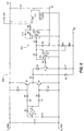
- FIG. 6 is a detailed schematic of a power supply and contrast control circuit 600 for an LCD display utilizing the present invention.
- Capacitors C 1 and C 2 provide filtering of IS_PWR and V CC , respectively.
- Elements U1, C3-C5, R1-R3, D1-D2 and Q1-Q2 form the oscillator for the charge pump of circuit 600.
- Schmitt trigger inverter U1, resistor R1 and capacitor C3 operate as a Schmitt trigger oscillator to generate a 5V square wave at about 600kHz at the output of Schmitt trigger inverter U 1.
- the 5V square wave at the output of Schmitt trigger inverter U 1 is AC coupled to the base-emitter diode of transistor Q1 and IS_PWR+ via diode D1 and capacitor C4.
- the 5V square wave at the output of Schmitt trigger inverter U is AC coupled to the base-emitter diode of transistor Q2 and IS_PWR- via diode D2 and capacitor C5.
- the single square output from Schmitt trigger inverter U1 drives both transistor Q1 and transistor Q2.
- the time constant formed by capacitor C4 and resistor R2 and by capacitor C5 and resistor R3 should be much longer than the oscillator period (approximately 1.6 ⁇ S) so that a clean square wave is presented to the bases of transistors Q1 and Q2.
- Resistors R2 and R3 also serve to limit the base current in transistors Q1 and Q2, respectively, to approximately 1mA.
- Transistors Q1 and Q2 form a push-pull driver. Since the same waveform drives the base of each, and transistor Q2 is NPN and transistor Q1 is PNP, they will turn on during alternate half-cycles of the base voltage. For purposes of describing the operation of the charge pump, assume that transistor Q3 is fully on. When transistor Q1 is on, capacitor C6 is charged up to IS_PWR (approximately 9V) less the collector-emitter saturation voltage of transistor Q1 and the forward voltage of diode D3. The sum of the two losses is approximately 0.7V.
- IS_PWR approximately 9V
- transistor Q1 When transistor Q1 turns off and transistor Q2 turns on, transistor Q2's collector is forced to ground and since no current can flow in the reverse direction through diode D3, the voltage across capacitor C6 is maintained and the cathode of diode D4 is forced to -9V. Current can then flow in the forward direction through diode D4, thus charge is transferred between capacitor C6 and capacitor C7.
- the output of the charge pump, V EE is dependent upon the voltage stored across capacitor C6 on the charging stroke of the oscillator.
- the output voltage V EE can be reduced by dropping the voltage at the collector of transistor Q 1 across an element in addition to capacitor C6.
- transistor Q3 is the additional element across which voltage is dropped to control the voltage across capacitor C6.
- the base voltage of transistor Q3 is determined by the output of op-amp U2 through resistor R4.
- V EE is divided down through resistors R5 and R6 as the feedback path to op-amp U2.
- a digital signal from a microprocessor (not shown) over path LDC_ADJ feeds a amplifier/filter stage 601 comprised of op-amp U3 resistors R7-R9 and capacitors C9-C10.
- the output of amplifier/filter stage 601 feeds the negative input of op-amp U2 while the divided down VEE voltage feeds the positive input of op-amp U2.
- the LCD contrast is thereby controlled to a desired level by controlling the voltage drop across transistor Q3.
- Negative voltage regulator VR1 provides an output of +5V at V CC .
- the overhead voltage (approximately -4V) of voltage regulator VR1 is added to the output of the charge pump circuit to produce V EE .
- Table 1 provides exemplary values for the preferred embodiment of circuit 600.
- An adjustable inverting voltage converter is described whereby the output of an inverting charge pump is controlled through a variable element that consumes a portion of the voltage supplied by the charge pump oscillator thereby leaving a controllable deficit of voltage on the charging capacitor.
- the inverting voltage converter is advantageously applied to contrast control of an LCD display.
Landscapes
- Engineering & Computer Science (AREA)
- Power Engineering (AREA)
- Dc-Dc Converters (AREA)
- Control Of Indicators Other Than Cathode Ray Tubes (AREA)
- Liquid Crystal Display Device Control (AREA)
- Control Of Electrical Variables (AREA)
- Control Of Positive-Displacement Pumps (AREA)
Claims (13)
- Einstellbarer Spannungswandler mit einem Oszillator (503), der zum Erzeugen eines oszillierenden Signals betrieben werden kann, und mit einer Ladungspumpe (500), die zum Erzeugen einer einstellbaren Ausgangsspannung aus einer im wesentlichen fixen externen Versorgungsspannung in Reaktion auf das oszillierende Signal sowie auf ein Steuersignal betrieben werden kann, wobei der Wandler umfasst:ein Ladungselement (C1) in der Ladungspumpe (500), das zum periodischen Entwickeln einer Ladungsspannung aus der externen Versorgungsspannung in Übereinstimmung mit dem oszillierenden Signal betrieben werden kann,ein Filterelement (C2) in der Ladungspumpe (500), das zum Empfangen der Ladung aus dem Ladungselement und zum Entwickeln der Ausgangsspannung aus derselben betrieben werden kann,eine Spannungssteuereinrichtung (501, 504) in der Ladungspumpe (500), die zusammen mit dem Ladungselement und in Reaktion auf das Steuersignal betrieben werden kann, um die Höhe der Ladungsspannung, die durch das Ladungselement empfangen wird, in Übereinstimmung mit dem Steuersignal einzustellen, um die Höhe der Ausgangsspannung aus dem Filterelement zu steuern.
- Spannungswandler nach Anspruch 1, wobei die Ladungspumpe umfasst:eine erste Schalteinrichtung (Q1, Q2) zum Anlegen der externen Versorgungsspannung an dem Ladungselement (C1) während eines ersten Halbzyklus des oszillierenden Signals, wodurch das Ladungselement (C1) auf die Ladungsspannung aufgeladen wird, undeine zweite Schalteinrichtung (Q1, Q2) zum Verbinden des Ladungselements (C1) mit dem Filterelement (C2) während eines zweiten Halbzyklus des oszillierenden Signals, um das Filterelement (C2) aufzuladen und dadurch die Ausgangsspannung an dem Filterelement (C2) zu erzeugen.
- Spannungswandler nach Anspruch 2, wobei die erste und die zweite Schalteinrichtung jeweils einen ersten und einen zweiten Transistor (Q1, Q2) umfassen.
- Spannungswandler nach Anspruch 2, wobei die erste und die zweite Schaiteinrichtung jeweils einen ersten und einen zweiten analogen Schalter (U1, U2) umfassen.
- Spannungswandler nach Anspruch 2:wobei die erste Schalteinrichtung einen PNP-Transistor (Q1) umfasst, dessen Emitter für die Verbindung mit einer ersten Leitung einer externen Stromversorgung konfiguriert ist, dessen Basis mit einem ersten Ausgang des Oszillators verbunden ist und dessen Kollektor mit einem Anschluss des Ladungselements verbunden ist, undwobei die zweite Schalteinrichtung einen NPN-Transistor (Q2) umfasst, dessen Emitter für die Verbindung mit einer zweiten Leitung der externen Stromversorgung konfiguriert ist, dessen Basis mit einem zweiten Ausgang des Oszillators verbunden ist und dessen Kollektor mit dem Anschluss des Ladungselements verbunden ist.
- Spannungswandler nach Anspruch 1, wobei die Spannungssteuereinrichtung umfasst:eine Einrichtung (504) zum Vergleichen der Ausgangsspannung mit einer Sollwertspannung, um ein Ausgabesteuersignal zu erzeugen, undeine Einrichtung (501), die auf die Vergleichseinrichtung reagiert, indem sie die Höhe der Ladungsspannung in Übereinstimmung mit dem Ausgabesteuersignal einstellt.
- Spannungswandler nach Anspruch 6, wobei die Spannungssteuereinrichtung eine abhängige Stromsenke (501) umfasst, die in Reihe mit dem Ladungselement (C1) geschaltet ist.
- Spannungswandler nach Anspruch 7, wobei die abhängige Stromsenke (501) einen Steuertransistor (Q3) umfasst, der in Reihe mit dem Ladungselement (C1) verbunden ist und auf das Ausgabesteuersignal reagiert, um die Spannung über den Steuertransistor zu variieren, so dass eine Erhöhung der Spannung über den Steuertransistor die Ladungsspannung reduziert.
- Spannungswandler nach Anspruch 6, wobei die Spannungsteuereinrichtung wenigstens einen variablen Widerstand (R4), einen variablen Kondensator (C6) und eine abhängige Spannungsquelle umfasst, die in Reihe mit dem Ladungselement verbunden sind.
- Spannungswandler nach Anspruch 6, der weiterhin eine Zener-Diode (D4) umfasst, die betrieben werden kann, um das Fließen von Ladung zu dem Ladungselement (C1) zu verhindern, wenn die zweite Schalteinrichtung geschlossen ist, wobei die Zener-Diode eine Anode, die mit dem Ladungselement verbunden ist, und eine Kathode aufweist, die mit der Spannungssteuereinrichtung verbunden ist.
- Spannungswandler nach Anspruch 1, der weiterhin eine Erdableitungseinrichtung zum Ableiten einer Erde in Bezug auf die externe Versorgungsspannung umfasst.
- Spannungswandler nach Anspruch 11, wobei die Erdungsableitungseinrichtung umfasst:
einen Spannungsregler, der konfiguriert ist, um die externe Versorgungsspannung zu empfangen und um eine geregelte Gleichstromspannung zu erzeugen, deren Erde eine fixe Spannung in Bezug auf die externe Versorgungsspannung aufweist. - Spannungswandler nach Anspruch 6, der weiterhin eine Erdableitungseinrichtung zum Ableiten einer Erde auf einem kontrollierten Pegel in Bezug auf die externe Stromversorgung umfasst, wobei die Erdableitungseinrichtung eine Überschussspannung erzeugt, die zu der Ausgabespannung addiert wird, um eine negative Spannung zu erzeugen, die zwischen der Überschussspannung und der Summe aus der Überschussspannung und der Ausgangsspannung eingestellt werden kann.
Applications Claiming Priority (3)
| Application Number | Priority Date | Filing Date | Title |
|---|---|---|---|
| US865052 | 1997-05-29 | ||
| US08/865,052 US5841648A (en) | 1997-05-29 | 1997-05-29 | Adjustable voltage converter utilizing a charge pump |
| PCT/US1998/009728 WO1998054825A1 (en) | 1997-05-29 | 1998-05-13 | Adjustable voltage converter utilizing a charge pump |
Publications (2)
| Publication Number | Publication Date |
|---|---|
| EP1016201A1 EP1016201A1 (de) | 2000-07-05 |
| EP1016201B1 true EP1016201B1 (de) | 2001-10-24 |
Family
ID=25344613
Family Applications (1)
| Application Number | Title | Priority Date | Filing Date |
|---|---|---|---|
| EP98921168A Expired - Lifetime EP1016201B1 (de) | 1997-05-29 | 1998-05-13 | Regelbarer spannungswandler mit ladungspumpe |
Country Status (9)
| Country | Link |
|---|---|
| US (1) | US5841648A (de) |
| EP (1) | EP1016201B1 (de) |
| JP (1) | JP3429009B2 (de) |
| CN (1) | CN1134884C (de) |
| AR (1) | AR012869A1 (de) |
| AU (1) | AU7384198A (de) |
| DE (1) | DE69802207T2 (de) |
| MY (1) | MY120744A (de) |
| WO (1) | WO1998054825A1 (de) |
Cited By (1)
| Publication number | Priority date | Publication date | Assignee | Title |
|---|---|---|---|---|
| RU2453029C1 (ru) * | 2011-03-30 | 2012-06-10 | Государственное образовательное учреждение высшего профессионального образования "Сибирский государственный индустриальный университет" | Регулируемый умножитель напряжения жмакина |
Families Citing this family (23)
| Publication number | Priority date | Publication date | Assignee | Title |
|---|---|---|---|---|
| US6574652B2 (en) * | 1994-10-18 | 2003-06-03 | M-I L.L.C. | Intrinsically safe communication and control system for use in hazardous locations including monotoring device with intrinsically safe fluorescent tube backlit |
| US6233285B1 (en) * | 1997-12-23 | 2001-05-15 | Honeywell International Inc. | Intrinsically safe cable drive circuit |
| US6466188B1 (en) * | 2000-01-20 | 2002-10-15 | International Business Machines Corporation | DC-DC converter with current sensing for use with non-linear devices |
| US6397322B1 (en) * | 2000-03-31 | 2002-05-28 | Schneider Automation, Inc. | Integrated intrinsically safe input-output module |
| DE10036283A1 (de) * | 2000-07-26 | 2002-02-07 | Bosch Gmbh Robert | Laserdiodenanordnung |
| JP4288849B2 (ja) * | 2000-12-06 | 2009-07-01 | ソニー株式会社 | アクティブマトリクス型表示装置およびこれを用いた携帯端末 |
| US6697402B2 (en) * | 2001-07-19 | 2004-02-24 | Analog Modules, Inc. | High-power pulsed laser diode driver |
| CN100353458C (zh) * | 2003-12-10 | 2007-12-05 | 上海华虹Nec电子有限公司 | 用于非挥发性存储器电路的电荷泵 |
| ATE410814T1 (de) * | 2004-05-07 | 2008-10-15 | Dialog Semiconductor Gmbh | Einsatz einer ladungspumpe mit tätiger entladefunktion |
| KR101061855B1 (ko) * | 2004-10-01 | 2011-09-02 | 삼성전자주식회사 | 구동 전압 생성 회로 및 이를 포함하는 표시 장치 |
| KR20070085048A (ko) * | 2004-12-03 | 2007-08-27 | 로무 가부시키가이샤 | 차지 펌프 회로의 구동 회로와 전원 장치 및 발광 장치 |
| US7687791B2 (en) | 2006-05-05 | 2010-03-30 | Pepperl & Fuchs (De) | Ethernet data signal transmission apparatus |
| FI120477B (fi) * | 2006-09-27 | 2009-10-30 | Vacon Oyj | Sähkömoottorin suojausjärjestely |
| US7330020B1 (en) * | 2006-10-11 | 2008-02-12 | Macronix International Co., Ltd. | Voltage regulation unit with zener diode and voltage regulation device thereof |
| US7898786B2 (en) * | 2007-01-26 | 2011-03-01 | Siemens Industry, Inc. | Intrinsically safe galvanically isolated barrier device and method thereof |
| US7868558B2 (en) * | 2007-11-21 | 2011-01-11 | General Electric Company | Organic light emitting diode power converter |
| TWI397044B (zh) * | 2008-08-06 | 2013-05-21 | Chunghwa Picture Tubes Ltd | 背光模組控制系統及其控制方法 |
| TWI399732B (zh) * | 2008-08-13 | 2013-06-21 | Sitronix Technology Corp | And a control chip for a color order type liquid crystal display device |
| US8207711B2 (en) * | 2008-08-15 | 2012-06-26 | Analog Modules, Inc. | Biphase laser diode driver and method |
| US8729870B2 (en) | 2008-08-15 | 2014-05-20 | Analog Modules, Inc. | Biphase laser diode driver and method |
| US20110278952A1 (en) | 2008-11-10 | 2011-11-17 | Nxp B.V. | Capacitive dc-dc converter |
| US8665577B2 (en) * | 2010-12-28 | 2014-03-04 | Lockheed Martin Corporation | Safe area voltage regulator |
| EP2824816A1 (de) | 2013-07-11 | 2015-01-14 | Dialog Semiconductor GmbH | DC/DC Wandler mit geschalteten Kapazitäten und niedrigem Eingangsstromrippel |
Family Cites Families (13)
| Publication number | Priority date | Publication date | Assignee | Title |
|---|---|---|---|---|
| US4236199A (en) * | 1978-11-28 | 1980-11-25 | Rca Corporation | Regulated high voltage power supply |
| JPS61281293A (ja) * | 1985-06-07 | 1986-12-11 | 株式会社東芝 | 液晶表示制御装置 |
| US4777577A (en) * | 1985-10-01 | 1988-10-11 | Maxim Integrated Products, Inc. | Integrated dual charge pump power supply and RS-232 transmitter/receiver |
| US4888677A (en) * | 1989-01-27 | 1989-12-19 | Teledyne Industries, Inc. | Three reservoir capacitor |
| US5132895A (en) * | 1990-12-11 | 1992-07-21 | Motorola, Inc. | Variable charge pumping DC-to-DC converter |
| US5306954A (en) * | 1992-06-04 | 1994-04-26 | Sipex Corporation | Charge pump with symmetrical +V and -V outputs |
| US5262934A (en) * | 1992-06-23 | 1993-11-16 | Analogic Corporation | Bipolar voltage doubler circuit |
| US5410465A (en) * | 1993-06-11 | 1995-04-25 | Tan; Charles M. C. | Integrated circuit charge pump voltage level converter |
| US5526253A (en) * | 1993-09-22 | 1996-06-11 | Advanced Micro Devices, Inc. | Low power voltage boost circuit with regulated output |
| US5486992A (en) * | 1995-01-09 | 1996-01-23 | The United States Of America As Represented By The Secretary Of The Army | High voltage direct current power supply with feedback control and circuit protection |
| US5606491A (en) * | 1995-06-05 | 1997-02-25 | Analog Devices, Inc. | Multiplying and inverting charge pump |
| US5699312A (en) * | 1996-04-18 | 1997-12-16 | Altera Corporation | Programmable voltage supply circuitry |
| US5625544A (en) * | 1996-04-25 | 1997-04-29 | Programmable Microelectronics Corp. | Charge pump |
-
1997
- 1997-05-29 US US08/865,052 patent/US5841648A/en not_active Expired - Lifetime
-
1998
- 1998-05-13 DE DE69802207T patent/DE69802207T2/de not_active Expired - Lifetime
- 1998-05-13 AU AU73841/98A patent/AU7384198A/en not_active Abandoned
- 1998-05-13 WO PCT/US1998/009728 patent/WO1998054825A1/en not_active Ceased
- 1998-05-13 EP EP98921168A patent/EP1016201B1/de not_active Expired - Lifetime
- 1998-05-13 JP JP50071399A patent/JP3429009B2/ja not_active Expired - Lifetime
- 1998-05-13 CN CNB988055627A patent/CN1134884C/zh not_active Expired - Lifetime
- 1998-05-27 AR ARP980102460A patent/AR012869A1/es active IP Right Grant
- 1998-05-28 MY MYPI98002384A patent/MY120744A/en unknown
Cited By (1)
| Publication number | Priority date | Publication date | Assignee | Title |
|---|---|---|---|---|
| RU2453029C1 (ru) * | 2011-03-30 | 2012-06-10 | Государственное образовательное учреждение высшего профессионального образования "Сибирский государственный индустриальный университет" | Регулируемый умножитель напряжения жмакина |
Also Published As
| Publication number | Publication date |
|---|---|
| JP3429009B2 (ja) | 2003-07-22 |
| EP1016201A1 (de) | 2000-07-05 |
| CN1258392A (zh) | 2000-06-28 |
| JP2002500858A (ja) | 2002-01-08 |
| WO1998054825A1 (en) | 1998-12-03 |
| HK1027684A1 (en) | 2001-01-19 |
| AU7384198A (en) | 1998-12-30 |
| US5841648A (en) | 1998-11-24 |
| AR012869A1 (es) | 2000-11-22 |
| MY120744A (en) | 2005-11-30 |
| DE69802207T2 (de) | 2002-04-18 |
| DE69802207D1 (de) | 2001-11-29 |
| CN1134884C (zh) | 2004-01-14 |
Similar Documents
| Publication | Publication Date | Title |
|---|---|---|
| EP1016201B1 (de) | Regelbarer spannungswandler mit ladungspumpe | |
| US4209826A (en) | Regulated switching mode power supply | |
| US5151017A (en) | Variable speed hydromassage pump control | |
| US7030572B2 (en) | Lighting arrangement | |
| US7019474B2 (en) | Constant current regulator using IGBT's with simplified timing | |
| EP0189221B1 (de) | Elektrische Schaltung für Regelung von Entladungslampen | |
| US3737756A (en) | Converter circuit with balanced parallel switching paths | |
| US5394017A (en) | Circuit for sustaining output power during input power interruption | |
| EP0165087A1 (de) | Getaktete Stromversorgung | |
| US4595977A (en) | Switched mode power supply | |
| US4755922A (en) | DC to DC converter for ethernet transceiver | |
| US4099099A (en) | Method of and switching device for reducing feedback from a consumer periodically connected to an A.C. line | |
| US5283441A (en) | Low-power current mirror having feedback with optical isolation | |
| US3736496A (en) | Energy pump voltage regulator | |
| GB2141563A (en) | Switching regulator off-line starting circuit | |
| GB2205699A (en) | Safety barriers for 2-wire transmitters | |
| WO1986001048A1 (en) | Switch-mode power supply | |
| EP0622890A2 (de) | Schaltnetzteilsystem für ferngesteuerte Fernsehempfänger oder dergleichen | |
| US5754415A (en) | Constant current flyback power supply having forward converter mode-configured auxiliary secondary windings producing constant voltage output | |
| US4922399A (en) | DC-to-DC converter having improved power supply arrangement | |
| US4755723A (en) | Strobe flash lamp power supply with afterglow prevention circuit | |
| EP0915611B1 (de) | Übertragerlose Speiseschaltung für digitale Teilnehmerleitungen | |
| EP0247407B1 (de) | Leistungsversorgung der Schaltungsart | |
| HK1027684B (en) | Adjustable voltage converter utilizing a charge pump | |
| US4924369A (en) | Regulated blocking converter wherein switch conduction time increases with higher output voltages |
Legal Events
| Date | Code | Title | Description |
|---|---|---|---|
| PUAI | Public reference made under article 153(3) epc to a published international application that has entered the european phase |
Free format text: ORIGINAL CODE: 0009012 |
|
| 17P | Request for examination filed |
Effective date: 19991025 |
|
| AK | Designated contracting states |
Kind code of ref document: A1 Designated state(s): DE |
|
| GRAG | Despatch of communication of intention to grant |
Free format text: ORIGINAL CODE: EPIDOS AGRA |
|
| 17Q | First examination report despatched |
Effective date: 20010108 |
|
| GRAG | Despatch of communication of intention to grant |
Free format text: ORIGINAL CODE: EPIDOS AGRA |
|
| GRAH | Despatch of communication of intention to grant a patent |
Free format text: ORIGINAL CODE: EPIDOS IGRA |
|
| GRAH | Despatch of communication of intention to grant a patent |
Free format text: ORIGINAL CODE: EPIDOS IGRA |
|
| GRAA | (expected) grant |
Free format text: ORIGINAL CODE: 0009210 |
|
| AK | Designated contracting states |
Kind code of ref document: B1 Designated state(s): DE |
|
| REF | Corresponds to: |
Ref document number: 69802207 Country of ref document: DE Date of ref document: 20011129 |
|
| PLBE | No opposition filed within time limit |
Free format text: ORIGINAL CODE: 0009261 |
|
| STAA | Information on the status of an ep patent application or granted ep patent |
Free format text: STATUS: NO OPPOSITION FILED WITHIN TIME LIMIT |
|
| 26N | No opposition filed | ||
| PGFP | Annual fee paid to national office [announced via postgrant information from national office to epo] |
Ref country code: DE Payment date: 20170530 Year of fee payment: 20 |
|
| REG | Reference to a national code |
Ref country code: DE Ref legal event code: R071 Ref document number: 69802207 Country of ref document: DE |