EP1015130B1 - Electroforming method for making a squeegee blade - Google Patents
Electroforming method for making a squeegee blade Download PDFInfo
- Publication number
- EP1015130B1 EP1015130B1 EP97923561A EP97923561A EP1015130B1 EP 1015130 B1 EP1015130 B1 EP 1015130B1 EP 97923561 A EP97923561 A EP 97923561A EP 97923561 A EP97923561 A EP 97923561A EP 1015130 B1 EP1015130 B1 EP 1015130B1
- Authority
- EP
- European Patent Office
- Prior art keywords
- squeegee blade
- stencil
- electroformed
- squeegee
- nickel
- Prior art date
- Legal status (The legal status is an assumption and is not a legal conclusion. Google has not performed a legal analysis and makes no representation as to the accuracy of the status listed.)
- Expired - Lifetime
Links
- 238000000034 method Methods 0.000 title claims abstract description 45
- 238000005323 electroforming Methods 0.000 title claims abstract description 12
- 229910000679 solder Inorganic materials 0.000 claims abstract description 71
- 239000000463 material Substances 0.000 claims abstract description 69
- 238000007639 printing Methods 0.000 claims abstract description 66
- 239000000758 substrate Substances 0.000 claims abstract description 26
- 238000004519 manufacturing process Methods 0.000 claims abstract description 18
- PXHVJJICTQNCMI-UHFFFAOYSA-N Nickel Chemical compound [Ni] PXHVJJICTQNCMI-UHFFFAOYSA-N 0.000 claims description 36
- 238000000151 deposition Methods 0.000 claims description 18
- 229910052759 nickel Inorganic materials 0.000 claims description 16
- XEEYBQQBJWHFJM-UHFFFAOYSA-N Iron Chemical compound [Fe] XEEYBQQBJWHFJM-UHFFFAOYSA-N 0.000 claims description 10
- 239000010935 stainless steel Substances 0.000 claims description 10
- 229910001220 stainless steel Inorganic materials 0.000 claims description 10
- VYZAMTAEIAYCRO-UHFFFAOYSA-N Chromium Chemical compound [Cr] VYZAMTAEIAYCRO-UHFFFAOYSA-N 0.000 claims description 6
- RYGMFSIKBFXOCR-UHFFFAOYSA-N Copper Chemical compound [Cu] RYGMFSIKBFXOCR-UHFFFAOYSA-N 0.000 claims description 6
- 239000011651 chromium Substances 0.000 claims description 6
- 229910052804 chromium Inorganic materials 0.000 claims description 6
- 239000010949 copper Substances 0.000 claims description 6
- 229910052802 copper Inorganic materials 0.000 claims description 6
- 229910052782 aluminium Inorganic materials 0.000 claims description 5
- XAGFODPZIPBFFR-UHFFFAOYSA-N aluminium Chemical compound [Al] XAGFODPZIPBFFR-UHFFFAOYSA-N 0.000 claims description 5
- 229910052742 iron Inorganic materials 0.000 claims description 5
- KDLHZDBZIXYQEI-UHFFFAOYSA-N Palladium Chemical compound [Pd] KDLHZDBZIXYQEI-UHFFFAOYSA-N 0.000 claims description 4
- RTAQQCXQSZGOHL-UHFFFAOYSA-N Titanium Chemical compound [Ti] RTAQQCXQSZGOHL-UHFFFAOYSA-N 0.000 claims description 4
- 239000010936 titanium Substances 0.000 claims description 4
- 229910052719 titanium Inorganic materials 0.000 claims description 4
- 229910045601 alloy Inorganic materials 0.000 claims description 3
- 239000000956 alloy Substances 0.000 claims description 3
- YOCUPQPZWBBYIX-UHFFFAOYSA-N copper nickel Chemical compound [Ni].[Cu] YOCUPQPZWBBYIX-UHFFFAOYSA-N 0.000 claims description 3
- -1 nickel-polytetrafluoroethylene Chemical group 0.000 claims description 3
- 229910000881 Cu alloy Inorganic materials 0.000 claims description 2
- 229910001252 Pd alloy Inorganic materials 0.000 claims description 2
- BQCADISMDOOEFD-UHFFFAOYSA-N Silver Chemical compound [Ag] BQCADISMDOOEFD-UHFFFAOYSA-N 0.000 claims description 2
- ATJFFYVFTNAWJD-UHFFFAOYSA-N Tin Chemical compound [Sn] ATJFFYVFTNAWJD-UHFFFAOYSA-N 0.000 claims description 2
- HCHKCACWOHOZIP-UHFFFAOYSA-N Zinc Chemical compound [Zn] HCHKCACWOHOZIP-UHFFFAOYSA-N 0.000 claims description 2
- QDWJUBJKEHXSMT-UHFFFAOYSA-N boranylidynenickel Chemical compound [Ni]#B QDWJUBJKEHXSMT-UHFFFAOYSA-N 0.000 claims description 2
- 229910017052 cobalt Inorganic materials 0.000 claims description 2
- 239000010941 cobalt Substances 0.000 claims description 2
- GUTLYIVDDKVIGB-UHFFFAOYSA-N cobalt atom Chemical compound [Co] GUTLYIVDDKVIGB-UHFFFAOYSA-N 0.000 claims description 2
- 239000002131 composite material Substances 0.000 claims description 2
- PCHJSUWPFVWCPO-UHFFFAOYSA-N gold Chemical compound [Au] PCHJSUWPFVWCPO-UHFFFAOYSA-N 0.000 claims description 2
- 229910052737 gold Inorganic materials 0.000 claims description 2
- 239000010931 gold Substances 0.000 claims description 2
- 239000011133 lead Substances 0.000 claims description 2
- 229910052763 palladium Inorganic materials 0.000 claims description 2
- 229910052709 silver Inorganic materials 0.000 claims description 2
- 239000004332 silver Substances 0.000 claims description 2
- 229910052718 tin Inorganic materials 0.000 claims description 2
- 239000011135 tin Substances 0.000 claims description 2
- 229910052725 zinc Inorganic materials 0.000 claims description 2
- 239000011701 zinc Substances 0.000 claims description 2
- 229920002120 photoresistant polymer Polymers 0.000 claims 2
- 229910000570 Cupronickel Inorganic materials 0.000 claims 1
- BHEPBYXIRTUNPN-UHFFFAOYSA-N hydridophosphorus(.) (triplet) Chemical compound [PH] BHEPBYXIRTUNPN-UHFFFAOYSA-N 0.000 claims 1
- 229910052751 metal Inorganic materials 0.000 abstract description 27
- 239000002184 metal Substances 0.000 abstract description 27
- 230000008021 deposition Effects 0.000 abstract description 14
- 230000008569 process Effects 0.000 description 16
- 229920002635 polyurethane Polymers 0.000 description 8
- 239000004814 polyurethane Substances 0.000 description 8
- 238000000576 coating method Methods 0.000 description 6
- 238000012360 testing method Methods 0.000 description 6
- 238000003486 chemical etching Methods 0.000 description 5
- 230000007547 defect Effects 0.000 description 5
- 230000009467 reduction Effects 0.000 description 5
- 229910021586 Nickel(II) chloride Inorganic materials 0.000 description 4
- 229910000831 Steel Inorganic materials 0.000 description 4
- KGBXLFKZBHKPEV-UHFFFAOYSA-N boric acid Chemical compound OB(O)O KGBXLFKZBHKPEV-UHFFFAOYSA-N 0.000 description 4
- 238000005516 engineering process Methods 0.000 description 4
- 238000011049 filling Methods 0.000 description 4
- 150000002500 ions Chemical class 0.000 description 4
- QMMRZOWCJAIUJA-UHFFFAOYSA-L nickel dichloride Chemical compound Cl[Ni]Cl QMMRZOWCJAIUJA-UHFFFAOYSA-L 0.000 description 4
- 229910001453 nickel ion Inorganic materials 0.000 description 4
- 238000007747 plating Methods 0.000 description 4
- 239000010959 steel Substances 0.000 description 4
- KFZMGEQAYNKOFK-UHFFFAOYSA-N Isopropanol Chemical compound CC(C)O KFZMGEQAYNKOFK-UHFFFAOYSA-N 0.000 description 3
- 230000008901 benefit Effects 0.000 description 3
- 238000007796 conventional method Methods 0.000 description 3
- 238000013461 design Methods 0.000 description 3
- 150000003071 polychlorinated biphenyls Chemical class 0.000 description 3
- 238000002360 preparation method Methods 0.000 description 3
- 238000012545 processing Methods 0.000 description 3
- 239000000047 product Substances 0.000 description 3
- 238000005476 soldering Methods 0.000 description 3
- 238000012546 transfer Methods 0.000 description 3
- 239000002699 waste material Substances 0.000 description 3
- 239000000654 additive Substances 0.000 description 2
- 239000011248 coating agent Substances 0.000 description 2
- 230000002860 competitive effect Effects 0.000 description 2
- 230000003247 decreasing effect Effects 0.000 description 2
- 239000012153 distilled water Substances 0.000 description 2
- 238000005530 etching Methods 0.000 description 2
- 238000007667 floating Methods 0.000 description 2
- 239000011888 foil Substances 0.000 description 2
- 230000006872 improvement Effects 0.000 description 2
- 238000003754 machining Methods 0.000 description 2
- 238000001465 metallisation Methods 0.000 description 2
- 150000002739 metals Chemical class 0.000 description 2
- 239000004033 plastic Substances 0.000 description 2
- 229920003023 plastic Polymers 0.000 description 2
- 238000007650 screen-printing Methods 0.000 description 2
- 239000002356 single layer Substances 0.000 description 2
- 238000005406 washing Methods 0.000 description 2
- XLYOFNOQVPJJNP-UHFFFAOYSA-N water Chemical compound O XLYOFNOQVPJJNP-UHFFFAOYSA-N 0.000 description 2
- 229920001875 Ebonite Polymers 0.000 description 1
- 239000004593 Epoxy Substances 0.000 description 1
- 229910001374 Invar Inorganic materials 0.000 description 1
- GRYLNZFGIOXLOG-UHFFFAOYSA-N Nitric acid Chemical compound O[N+]([O-])=O GRYLNZFGIOXLOG-UHFFFAOYSA-N 0.000 description 1
- DBMJMQXJHONAFJ-UHFFFAOYSA-M Sodium laurylsulphate Chemical compound [Na+].CCCCCCCCCCCCOS([O-])(=O)=O DBMJMQXJHONAFJ-UHFFFAOYSA-M 0.000 description 1
- XSTXAVWGXDQKEL-UHFFFAOYSA-N Trichloroethylene Chemical group ClC=C(Cl)Cl XSTXAVWGXDQKEL-UHFFFAOYSA-N 0.000 description 1
- JUWOETZNAMLKMG-UHFFFAOYSA-N [P].[Ni].[Cu] Chemical compound [P].[Ni].[Cu] JUWOETZNAMLKMG-UHFFFAOYSA-N 0.000 description 1
- 150000001450 anions Chemical class 0.000 description 1
- 230000003466 anti-cipated effect Effects 0.000 description 1
- 239000011230 binding agent Substances 0.000 description 1
- 239000006172 buffering agent Substances 0.000 description 1
- 239000000969 carrier Substances 0.000 description 1
- 238000005266 casting Methods 0.000 description 1
- 239000003054 catalyst Substances 0.000 description 1
- 150000001768 cations Chemical class 0.000 description 1
- 239000003153 chemical reaction reagent Substances 0.000 description 1
- 239000003795 chemical substances by application Substances 0.000 description 1
- 238000004140 cleaning Methods 0.000 description 1
- 230000000052 comparative effect Effects 0.000 description 1
- 230000000295 complement effect Effects 0.000 description 1
- 229920001940 conductive polymer Polymers 0.000 description 1
- 239000004020 conductor Substances 0.000 description 1
- 230000007797 corrosion Effects 0.000 description 1
- 238000005260 corrosion Methods 0.000 description 1
- 238000005520 cutting process Methods 0.000 description 1
- 230000000593 degrading effect Effects 0.000 description 1
- 238000005238 degreasing Methods 0.000 description 1
- 238000005137 deposition process Methods 0.000 description 1
- 238000011161 development Methods 0.000 description 1
- 238000011143 downstream manufacturing Methods 0.000 description 1
- 230000000694 effects Effects 0.000 description 1
- 230000008030 elimination Effects 0.000 description 1
- 238000003379 elimination reaction Methods 0.000 description 1
- 125000003700 epoxy group Chemical group 0.000 description 1
- 239000012467 final product Substances 0.000 description 1
- 230000004907 flux Effects 0.000 description 1
- 239000002529 flux (metallurgy) Substances 0.000 description 1
- 238000000227 grinding Methods 0.000 description 1
- 229910001026 inconel Inorganic materials 0.000 description 1
- 239000000976 ink Substances 0.000 description 1
- 238000003698 laser cutting Methods 0.000 description 1
- 239000010410 layer Substances 0.000 description 1
- 230000007246 mechanism Effects 0.000 description 1
- 239000000203 mixture Substances 0.000 description 1
- 238000012986 modification Methods 0.000 description 1
- 230000004048 modification Effects 0.000 description 1
- 238000000465 moulding Methods 0.000 description 1
- 238000009740 moulding (composite fabrication) Methods 0.000 description 1
- 229910017604 nitric acid Inorganic materials 0.000 description 1
- 238000004806 packaging method and process Methods 0.000 description 1
- OFNHPGDEEMZPFG-UHFFFAOYSA-N phosphanylidynenickel Chemical compound [P].[Ni] OFNHPGDEEMZPFG-UHFFFAOYSA-N 0.000 description 1
- 229920000647 polyepoxide Polymers 0.000 description 1
- 230000008439 repair process Effects 0.000 description 1
- 238000011160 research Methods 0.000 description 1
- 150000003839 salts Chemical class 0.000 description 1
- 238000012216 screening Methods 0.000 description 1
- 238000010008 shearing Methods 0.000 description 1
- 235000019333 sodium laurylsulphate Nutrition 0.000 description 1
- 239000002904 solvent Substances 0.000 description 1
- IIACRCGMVDHOTQ-UHFFFAOYSA-M sulfamate Chemical compound NS([O-])(=O)=O IIACRCGMVDHOTQ-UHFFFAOYSA-M 0.000 description 1
- FZUJWWOKDIGOKH-UHFFFAOYSA-N sulfuric acid hydrochloride Chemical compound Cl.OS(O)(=O)=O FZUJWWOKDIGOKH-UHFFFAOYSA-N 0.000 description 1
- 239000004094 surface-active agent Substances 0.000 description 1
- 231100000331 toxic Toxicity 0.000 description 1
- 230000002588 toxic effect Effects 0.000 description 1
- 239000010891 toxic waste Substances 0.000 description 1
- UBOXGVDOUJQMTN-UHFFFAOYSA-N trichloroethylene Natural products ClCC(Cl)Cl UBOXGVDOUJQMTN-UHFFFAOYSA-N 0.000 description 1
- 238000007740 vapor deposition Methods 0.000 description 1
- 238000011179 visual inspection Methods 0.000 description 1
Images

Classifications
-
- B—PERFORMING OPERATIONS; TRANSPORTING
- B41—PRINTING; LINING MACHINES; TYPEWRITERS; STAMPS
- B41C—PROCESSES FOR THE MANUFACTURE OR REPRODUCTION OF PRINTING SURFACES
- B41C1/00—Forme preparation
- B41C1/14—Forme preparation for stencil-printing or silk-screen printing
-
- B—PERFORMING OPERATIONS; TRANSPORTING
- B41—PRINTING; LINING MACHINES; TYPEWRITERS; STAMPS
- B41F—PRINTING MACHINES OR PRESSES
- B41F15/00—Screen printers
- B41F15/14—Details
- B41F15/40—Inking units
- B41F15/42—Inking units comprising squeegees or doctors
-
- B—PERFORMING OPERATIONS; TRANSPORTING
- B41—PRINTING; LINING MACHINES; TYPEWRITERS; STAMPS
- B41N—PRINTING PLATES OR FOILS; MATERIALS FOR SURFACES USED IN PRINTING MACHINES FOR PRINTING, INKING, DAMPING, OR THE LIKE; PREPARING SUCH SURFACES FOR USE AND CONSERVING THEM
- B41N10/00—Blankets or like coverings; Coverings for wipers for intaglio printing
- B41N10/005—Coverings for wipers
-
- H—ELECTRICITY
- H05—ELECTRIC TECHNIQUES NOT OTHERWISE PROVIDED FOR
- H05K—PRINTED CIRCUITS; CASINGS OR CONSTRUCTIONAL DETAILS OF ELECTRIC APPARATUS; MANUFACTURE OF ASSEMBLAGES OF ELECTRICAL COMPONENTS
- H05K3/00—Apparatus or processes for manufacturing printed circuits
- H05K3/10—Apparatus or processes for manufacturing printed circuits in which conductive material is applied to the insulating support in such a manner as to form the desired conductive pattern
- H05K3/12—Apparatus or processes for manufacturing printed circuits in which conductive material is applied to the insulating support in such a manner as to form the desired conductive pattern using thick film techniques, e.g. printing techniques to apply the conductive material or similar techniques for applying conductive paste or ink patterns
- H05K3/1216—Apparatus or processes for manufacturing printed circuits in which conductive material is applied to the insulating support in such a manner as to form the desired conductive pattern using thick film techniques, e.g. printing techniques to apply the conductive material or similar techniques for applying conductive paste or ink patterns by screen printing or stencil printing
- H05K3/1233—Methods or means for supplying the conductive material and for forcing it through the screen or stencil
-
- H—ELECTRICITY
- H05—ELECTRIC TECHNIQUES NOT OTHERWISE PROVIDED FOR
- H05K—PRINTED CIRCUITS; CASINGS OR CONSTRUCTIONAL DETAILS OF ELECTRIC APPARATUS; MANUFACTURE OF ASSEMBLAGES OF ELECTRICAL COMPONENTS
- H05K2203/00—Indexing scheme relating to apparatus or processes for manufacturing printed circuits covered by H05K3/00
- H05K2203/01—Tools for processing; Objects used during processing
- H05K2203/0104—Tools for processing; Objects used during processing for patterning or coating
- H05K2203/0139—Blade or squeegee, e.g. for screen printing or filling of holes
Definitions
- the present invention relates to a method of fabricating an electroformed squeegee blade used for the uniform deposition of printing material on printed wiring boards and/or printed circuit boards (PWBs or PCBs).
- PWBs or PCBs printed circuit boards
- the printing apparatus typically comprises a screen printer, a stencil, and a squeegee blade assembly.
- Various printing materials may be applied to a substrate by the application of printing material through stencil apertures on to the substrate.
- stencil apertures match the shape of PWB/PCB pads and are at the same locations as the PWB/PCB pad image array to be applied.
- the stencil images are aligned with the PWB/PCB images to be applied, placed in intimate contact with the PWB/PCB and held firmly together with the PWB/PCB until after the print stroke is completed.
- solder paste that forms the solder pads is applied to the top surface of the stencil.
- the squeegee blade is then used to draw the solder paste over the entire stencil image area, push the solder paste into the corresponding apertures of the stencil and form the solder deposition on the PWB pads.
- the component to be mounted is then placed directly into the wet solder paste.
- U.S. Patent No. 5,254,362 to Shaffer et al. relates to a method and apparatus for depositing solder paste on a printed wiring board. The method involves the vibration of a squeegee blade assembly by a vibrator to produce a slight circular motion in addition to the planar motion of the squeegee blade.
- U.S. patent No. 5,044,306 to Erdmann relates to a method of using two squeegee blades for wiping solder paste onto a printed wiring board.
- the method involves using a first squeegee to wipe solder paste across a stencil in combination with a second squeegee that cooperates with a tray to deposit solder paste at the beginning of a wiping stroke.
- the tray also cooperates with the first squeegee to pick up excess solder paste at the end of a wiping stroke.
- the squeegee blades available in the market place today are typically manufactured from high density polyurethane or stainless steel in a stamping, cutting or etching process. These squeegee blades are sometimes treated with alternate coatings and processes with the intention of improving the solder paste deposition process.
- polyurethane squeegee blades are designed to be somewhat flexible, thereby readily deforming to the stencil surface.
- the inherent compliance of polyurethane squeegee blades is desirable in certain applications, for example, step or multi-level stencils. In the use of step or multi-level stencils, compliance with the stencil surface has proven advantageous.
- deformation of the blade edge is disadvantageous due to aperture scooping occurring during the printing process. scooping is the result of polyurethane blade material compliance or deformation extending beyond the top plane of the stencil into an aperture and removing (scooping) solder paste out of the aperture during the squeegee print stroke. Scooping is a major cause of insufficient solder joints and the associated problems that result from insufficient solder joints.
- Reduced squeegee compliance, deformation and scooping are achieved by using a less flexible blade material.
- the more rigid, less compliant material of choice for squeegee blades has been stainless steel.
- print quality is improved by using metal squeegee blades, thereby yielding a more controlled and consistent print height across the entire image area, a better definition of the solder paste deposition on the PCB/PWB pads, a minimized amount of "scooping" and an overall improved aperture filling.
- Many of the negative effects of polyurethane squeegee blades are thus overcome with metal blades.
- metal squeegee blades offer improved printing results, they are not ideal in all aspects due to sticking or adhesion of printing material to the metal blade.
- Research to combat the inherent incompatibility of the metal squeegee blade with metal stencils as well as the tendency of printing materials and solder paste to stick to the metal squeegee blade has thus been conducted.
- various alternative and specialty coatings as well as secondary plating process steps have been explored to minimize the adherence or sticking of solder paste to the squeegee blades.
- the adherence of print material or solder paste to the squeegee blade has a profound negative impact on the consistency and quality of the resultant deposition on the PWB/PCB.
- Additional conventional methods of fabricating squeegee blades include casting from a mold and machining. These methods may require a finishing step to produce the final product.
- chemical etching a subtractive fabrication process, wherein characteristic surface features are formed when a polished metal surface is etched by suitable reagents, has been used. Chemical etching as a manufacturing process has characteristics that limit its use in high, tolerance, high precision applications.
- electropolishing Another conventional technique is electropolishing. This technique starts with a chemically etched squeegee blade as described earlier. and adds. an electrochemical etching process that, in theory, smooths the surface of the, squeegee blade. The electropolished surface does help solder paste release, to a certain degree when compared to a non-electropolished surface.
- a typical electropolished squeegee blade still has most of the drawbacks associated with a chemically etched squeegee blade.
- electropolishing minimizes the imperfections introduced by chemical etching, it is unable to completely compensate for them and the drawbacks associated with chemical etching are carried forward to the finished product even after electropolishing.
- solder paste adhering or sticking to the blade causes the solder paste to be pulled out of the previously filled aperture, thereby showing signs of lifting or "tailing" of printing material out of the aperture on the trailing edge of the print stroke.
- Incompatibility between metal squeegee blade and printing material, lower solder paste shearing forces, lower lubricity and a tendency toward solder paste sticking introduce significant inconsistency into the printing process.
- Control of the solder paste can become a problem depending on the ratio of the aperture width and thickness of the stencil. This is because up to 70% of the printing material or solder paste adheres to the squeegee blade rather than depositing on the board.
- stencil offset is caused by friction between the squeegee blade and the stencil. During the printing cycle, the stencil can be offset in the direction of the squeegee blade print stroke, thus offsetting the stencil aperture image relative to the PCB/PWB pads with which they are intended to register.
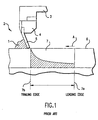
- FIG. 1 depicts a prior art application of solder paste 1 by a solder paste application machine 2.
- the solder paste application machine 2 can be a Model SP 200 screen printer by MPM Corporation (Franklin, MA) or an equivalent.
- FIG. 1 depicts the machine 2, which is connected to and controls squeegee blade assembly 3 including squeegee blade holder 4 and squeegee blade 5 made of stainless steel, plated stainless steel, propriety specialty coated stainless steel or polyurethane.
- Squeegee blade assembly 3 may be either a floating or non-floating head assembly.
- the squeegee blade 5 is shown in position, after having been drawn across the stencil 6.
- An amount of solder paste 1 is shown still adjacent to the squeegee blade 5. This solder paste 1 is in excess of the amount deposited and has been drawn across the stencil 6 in the direction indicated by the arrow A.
- the stencil aperture 7 is filled with solder paste 1.
- the amount of solder paste 1 is much less than the amount of solder paste 1 at the trailing edge 7b (i.e., the last edge of an aperture to be contacted by the squeegee blade 5) of the stencil aperture 7.
- surface mounted components (not shown), which are mounted to a printed wiring board (not shown) upon which solder paste 1 has been deposited may move, losing effective electrical contact with the desired circuit(s) or even becoming disconnected from solder paste 1 due to uneven application of solder paste 1. Therefore, such application of solder paste 1 is inappropriate to securely and effectively fasten surface mounted components to printed wiring boards.
- printing material or solder paste should be deposited evenly across the entire stencil image area. If the solder paste deposition is not uniform, components mounted in such an arrangement may shift, move or become dislodged with subsequent PWB processing.
- the invention is directed to a method of fabricating an electroformed squeegee blade according to claim 1, suitable for screen printing and other applications in which a smooth squeegee blade is suitable.
- the method for preparing the electroformed squeegee blade according to the invention involves electroforming at least one uniform layer of metal. A variety of blade edge designs and various blade edge thicknesses that allow for user definable printing characteristics could be prepared. Thus, electroformed squeegee blades permit the manufacture and use of multiple layer designs and a wide variety of blade edges that are custom fit to the printing application and printing materials being used.
- the method according to the invention eliminates any requirement for secondary processing, additional finishing, specialty coating or plating steps.
- the method thus produces smooth, planar, and flat surfaces without additional lapping, grinding, forming, or machining to obtain flatness or planarity.
- the electroformed squeegee blade prepared according to the invention is more compatible with stencil materials due to increased lubricity and decreased friction between the electroformed squeegee blade and the stencil.
- Electroformed squeegee blades are used in the printing operation of the electronics packaging industry, and more particularly in surface mount manufacturing. Unlike conventional methods of producing squeegee blades, squeegee blades made according to the invention are grown atom by atom with an electroforming process that utilizes specialized chemistries and process conditions that render the squeegee blade with improved properties and characteristics related to the squeegee blade application.
- Print tests using the electroformed squeegee blade made according to the invention show a minimum 75% reduction in the amount of residual print material left on the stencil after each print cycle. The result is a reduction in the build-up of dzied material clogging stencil apertures and improved print definition.
- the enhanced printing consistency that results from the use of an electroformed squeegee blade made according to the invention reduces the occurrence of bridging, bleed-out and insufficient aperture filling, key causes of manufacturing defects. By reducing the number of defects associated with stencil printing, a reduction in manufacturing costs is achieved.
- stencil wear normally associated with the printing operation is reduced. printing tests performed with current technology metal squeegee blades show stencil coining and wear by visual inspection, while electroformed squeegee blades exhibit little or no wear at all after an equal number of printing cycles on a test stencil.
- a major cause of the coining and wear seen for the current technology metal squeegee blades introduced during the manufacturing process is a lack of blade edge planarity.
- the electroformed squeegee blade fabricated according to the invention provides enhanced squeegee blade edge planarity that has been unachievable under current chemical etching, laser cutting, molding or secondary processing steps.
- the life expectancy of the stencil is anticipated to increase by 200%.
- Another benefit of the electroformed squeegee blade fabricated according to the invention is that as the surface tension attributed to the squeegee blade is reduced, the tendency of the printing material to stick to the squeegee blade is minimized. This is a problem most noticeable during the use of two squeegee blades as the direction of squeegee blade travel is changed and a switch from front to rear or rear to front squeegee blades is made. The result is often a smearing of the printing material, presenting an opportunity for the introduction of printing defects. With an electroformed squeegee blade, the printing material has a tendency to roll into a uniform cylindrical mass ahead of the squeegee blade during printing.
- the cylindrical mass of printing material is left on the stencil, precisely aligned for the next print stroke. As a result, 30% less printing material is required to be applied to the stencil and waste is reduced. This more efficient use of printing material or solder paste reduces waste and improves the overall print deposition quality, uniformity and consistency.
- an electroformed squeegee blade made in accordance with the invention required a reduced amount of solder paste printing material relative to that of conventional squeegee blades. This is due to a minimization of sticking of the printing material to the squeegee blade, an elimination of accumulating or piling of printing material along the side of the stencil image outside of the squeegee's reach, and an overall cleaner stencil surface. In addition, improvement is achieved due to a consistent volume of paste being available across the whole stencil image area, which further enhances printing performance.
- the method of the invention which is a variation of the method disclosed in U.S. Patent No. 5,478,699 to Blessington deceased, et al., involves electrodepositing metal on a conductive substrate.
- Typical substrate materials include stainless steel, iron plated with chromium or nickel, nickel, copper, titanium, aluminum, aluminum plated with chromium or nickel, titanium palladium alloys, nickel-copper alloys such as Inconel® 600 and Invar® (available from Inco, Saddle Brook, New Jersey and the like.
- Non-metallic substrates can also be used if they have been made conductive, for example, by being appropriately metallized using metallization techniques known to the art, such as electroless metallization, vapor deposition, and the like. A conductive substrate is first cleaned by methods well known to those of skill in the art.
- the sequence of cleaning steps can include washing with isopropyl alcohol, vapor degreasing in trichloroethylene, electrocleaning, rinsing in distilled water, washing in nitric acid, and final rinsing in distilled water.
- the process takes place within an electroforming zone comprising an anode, a cathode, and an electroforming bath.
- the bath may be composed of: ions or salts of ions of the layer-forming material, the concentration of which can range from trace to saturation, which ions can be in the form of anions or cations; a solvent; a buffering agent, the concentration of which can range from zero to saturation; an anode corrosion agent, the concentration of which can range from zero to saturation; and, optionally, grain refiners, levelers, catalysts, surfactants, and other additives known in the art.
- the preferred concentration ranges may readily be established by those of skill in the art without undue experimentation.
- a preferred electroforming bath to plate nickel on a substrate comprises about 70-90 mg/ml of nickel ion in solution, about 20-40 mg/ml of H 3 BO 3 , about 3.0 mg/ml of NiCl 2 ⁇ 6H 2 O and about 4.0-6.0 ml/liter of sodium lauryl sulfate.
- electroforming bath compositions include, but are not limited to, Watts nickel: about 68-88 mg/ml of nickel ion, about 50-70 mg/ml of NiCl 2 ⁇ 6H 2 O and about 20-40 mg/ml of H 3 BO 3 ; chloride sulfate: about 70-100 mg/ml of nickel ion, about 145-170 mg/ml of NiCl 2 ⁇ 6H 2 O and about 30-45 mg/ml H 3 BO 3 ; and concentrated sulfamate: about 100-120 mg/ml of nickel ion, about 3-10 mg/ml of NiCl 2 ⁇ 6H 2 O and about 30-45 mg/ml of H 3 BO 3 .
- Electroless baths such as electroless. nickel baths can also be employed. Various types are available depending upon the properties required in the electroform deposition. These electroless baths are well known to those skilled in the art.
- metals that can be electroformed onto the surface of a substrate include, but are not limited to, nickel, copper, gold, silver, palladium, tin, lead, chromium, zinc, cobalt, iron, and alloys thereof.
- Preferred metals are nickel and copper.
- Any suitable conductor or material that can be electrochemically deposited can be used, such as conductive polymers, plastics, and electroless nickel deposits.
- suitable autocatalytic electroless nickel deposits include, but are not limited to, nickel-phosphorus, nickel-boron, poly-alloys, such as copper-nickel phosphorus, nickel-polytetrafluoroethylene, composite coatings, and the like. Methods of preparing electroless nickel deposits employed within the scope of this invention are well known to those skilled in the art of electroforming.
- the electrolytic bath is energized using a suitable electrical source.
- Layer-forming ions from the solution are electroformed onto the conductive surface of the substrate.
- the process is allowed to proceed until a single layer has deposited on the substrate preferably ranging in thickness from about 0.200 to about 0.385mm.
- the substrate is removed from the solution.
- a squeegee blade having desired features can be prepared using a pattern of resist having a design complementary to the desired features in accordance with the process disclosed in U.S. Patent No. 5,478,699.
- the electroformed squeegee blade 5 made according to the invention causes the solder paste 1 to be applied to a uniform vertical height in the stencil apertures 7 regardless of their orientation.
- the solder pads 8 are uniformly deposited on the printed wiring board 9 of FIG. 2.
- the printed wiring board 9 is. firmly held in place beneath the stencil 6 by, e.g., suction, tooling holes, adjustable mechanical fixturing or dedicated mechanical fixturing and after the deposition of the solder paste 1 is then released to the next operation in the printed wiring board manufacturing process.
- the printed wiring board 9 with solder pads 8 produced according to the invention will more firmly hold surface mounted integrated circuits and/or components to the printed wiring board 9 for subsequent mounting and soldering flow operations.
- the electroformed squeegee blade made according to the invention which has an HK 500 hardness preferably about 200 to 600, and more preferably of about 390 to 450, permits a more uniform deposition of solder paste on the printed wiring board. As a result, the number of printed wiring boards that must be reworked for solder pad faults and integrated circuit mountings is minimal.
Landscapes
- Engineering & Computer Science (AREA)
- Manufacturing & Machinery (AREA)
- Microelectronics & Electronic Packaging (AREA)
- Mechanical Engineering (AREA)
- Screen Printers (AREA)
- Electric Connection Of Electric Components To Printed Circuits (AREA)
- Mechanical Treatment Of Semiconductor (AREA)
- Manufacturing Of Printed Wiring (AREA)
- Crystals, And After-Treatments Of Crystals (AREA)
- Physical Vapour Deposition (AREA)
- Polishing Bodies And Polishing Tools (AREA)
- Electrolytic Production Of Metals (AREA)
- Electrodes For Compound Or Non-Metal Manufacture (AREA)
Abstract
Description
- The present invention relates to a method of fabricating an electroformed squeegee blade used for the uniform deposition of printing material on printed wiring boards and/or printed circuit boards (PWBs or PCBs).
- Screen printing apparatus, which have a wide variety of uses in the electronic substrate fabrication and electronic assembly industries, are well known as exemplified by U.S. Patents Nos. 5,478,699; 3,930,455; 5,387,044; 5,357,856 and 5,323,700. These uses include, but are not limited to, the deposition of printing material, such as solder paste, conductive epoxies, thermal set plastics, conductive/resistive inks and the like, in the preparation of surface mount PCBs, Flip Chip Bumping, Co-Fired Via Fill, BGA, conductive/resistive circuit applications and the like.
- The printing apparatus typically comprises a screen printer, a stencil, and a squeegee blade assembly. Various printing materials may be applied to a substrate by the application of printing material through stencil apertures on to the substrate. For example, in the preparation of printed wiring boards (PWBs) for the placement of surface mounted components, solder paste is deposited on the PWB through stencil apertures. The stencil apertures match the shape of PWB/PCB pads and are at the same locations as the PWB/PCB pad image array to be applied. The stencil images are aligned with the PWB/PCB images to be applied, placed in intimate contact with the PWB/PCB and held firmly together with the PWB/PCB until after the print stroke is completed. An amount of solder paste that forms the solder pads is applied to the top surface of the stencil. The squeegee blade is then used to draw the solder paste over the entire stencil image area, push the solder paste into the corresponding apertures of the stencil and form the solder deposition on the PWB pads. The component to be mounted is then placed directly into the wet solder paste.
- As the electronics industry has progressed over the past few years, the trend has been towards the use of more complex devices and smaller circuits. A concern in the soldering of components is to consistently provide the precise volume of solder to the PWB/PCB pad sites to form effective solder joints. It is imperative that the amount/volume of solder paste applied to each PCB/PWB soldering pad is consistent and uniform so that the lowest possible defect levels in manufacturing is maintained. An inadequate amount of solder due to incomplete aperture filling during the squeegee printing stroke can lead to problems in forming consistent, uniform and reliable electromechanical solder joints. Excessive solder due to the overfilling of stencil apertures during the squeegee printing stroke can result in shorting or "bridging" between complex components, for example, QFPs, TSOPs, etc., pins or leads, resulting in problems in forming consistent, uniform and reliable solder joints. Both insufficient and excessive solder paste deposits lead to increased repair, and rework requirements, high overall. manufacturing costs, as well as finished product quality/reliability issues due to random variation from documented industry standard solder joint specifications.
- Efforts have thus focused on the development of materials that are better suited for fine pitch screening processes. One example is the introduction of new types of apparatus to aid movement of the solder paste over the aperture. For example, U.S. Patent No. 5,254,362 to Shaffer et al. relates to a method and apparatus for depositing solder paste on a printed wiring board. The method involves the vibration of a squeegee blade assembly by a vibrator to produce a slight circular motion in addition to the planar motion of the squeegee blade. U.S. patent No. 5,044,306 to Erdmann relates to a method of using two squeegee blades for wiping solder paste onto a printed wiring board. The method involves using a first squeegee to wipe solder paste across a stencil in combination with a second squeegee that cooperates with a tray to deposit solder paste at the beginning of a wiping stroke. The tray also cooperates with the first squeegee to pick up excess solder paste at the end of a wiping stroke.
- Another example of such efforts is the introduction of new types of sgueegee blades. See, for example, U.S. Patent No. 5,078,082 to van Dyk Soerewn and Hall, Developing a Low PPM Defect Level Ultra-Fine Pitch Process, New Technologies for Perfect Printing, User's Guide to More precise SMT Printing, MPM Corporation, pp. 12-21 (1994).
- In place of the traditional hard rubber blades, the squeegee blades available in the market place today are typically manufactured from high density polyurethane or stainless steel in a stamping, cutting or etching process. These squeegee blades are sometimes treated with alternate coatings and processes with the intention of improving the solder paste deposition process.
- The use of stainless steel squeegee blades has enabled a more controlled and consistent print height across the entire board area. However, as disclosed in Freeman, New Technologies for Perfect Printing, User's Guide to More Precise SMT Printing, MPM Corporation, pp. 22-29 (1994), "any irregularities in the circuit board surface can cause damage to the fine webs in the fine pitch areas, since steel is not 'forgiving.' In addition, steel lacks lubricity, causing greater wear on the stencil." Thus, room for improvement remains.
- polyurethane squeegee blades are designed to be somewhat flexible, thereby readily deforming to the stencil surface. The inherent compliance of polyurethane squeegee blades is desirable in certain applications, for example, step or multi-level stencils. In the use of step or multi-level stencils, compliance with the stencil surface has proven advantageous. At the same time, however, deformation of the blade edge is disadvantageous due to aperture scooping occurring during the printing process. scooping is the result of polyurethane blade material compliance or deformation extending beyond the top plane of the stencil into an aperture and removing (scooping) solder paste out of the aperture during the squeegee print stroke. Scooping is a major cause of insufficient solder joints and the associated problems that result from insufficient solder joints.
- Reduced squeegee compliance, deformation and scooping are achieved by using a less flexible blade material. The more rigid, less compliant material of choice for squeegee blades has been stainless steel. print quality is improved by using metal squeegee blades, thereby yielding a more controlled and consistent print height across the entire image area, a better definition of the solder paste deposition on the PCB/PWB pads, a minimized amount of "scooping" and an overall improved aperture filling. Many of the negative effects of polyurethane squeegee blades are thus overcome with metal blades.
- Although metal squeegee blades offer improved printing results, they are not ideal in all aspects due to sticking or adhesion of printing material to the metal blade. Research to combat the inherent incompatibility of the metal squeegee blade with metal stencils as well as the tendency of printing materials and solder paste to stick to the metal squeegee blade has thus been conducted. For example, various alternative and specialty coatings as well as secondary plating process steps have been explored to minimize the adherence or sticking of solder paste to the squeegee blades. The adherence of print material or solder paste to the squeegee blade has a profound negative impact on the consistency and quality of the resultant deposition on the PWB/PCB. Printing material additives such as tackifiers, binders, carriers and fluxes added for improved downstream process performance, increase the adherence of print material to the squeegee blade. Secondary surface preparation steps such as plating and specialty coatings improve the release characteristics of metal squeegee blades to some degree. The drawback of current metal squeegee blades that are processed through a secondary step is that with repeated use, the specialty coating or plating is worn away exposing the underlying bare metal and causing the recurrence of solder paste sticking or adhesion problems. The exposed bare metal increases the occurrence of insufficient or excessive solder paste, which in turn, affects the performance of the metal squeegee blade, thereby degrading the consistency, reliability and overall quality of the printing process.
- Additional conventional methods of fabricating squeegee blades include casting from a mold and machining. These methods may require a finishing step to produce the final product. In addition, chemical etching, a subtractive fabrication process, wherein characteristic surface features are formed when a polished metal surface is etched by suitable reagents, has been used. Chemical etching as a manufacturing process has characteristics that limit its use in high, tolerance, high precision applications.
- Another conventional technique is electropolishing. This technique starts with a chemically etched squeegee blade as described earlier. and adds. an electrochemical etching process that, in theory, smooths the surface of the, squeegee blade. The electropolished surface does help solder paste release, to a certain degree when compared to a non-electropolished surface. However, a typical electropolished squeegee blade still has most of the drawbacks associated with a chemically etched squeegee blade. Thus, although electropolishing minimizes the imperfections introduced by chemical etching, it is unable to completely compensate for them and the drawbacks associated with chemical etching are carried forward to the finished product even after electropolishing.
- Difficulties observed during the use of conventional squeegee blades include negative wear characteristics, incompatibility with stencil materials, incompatibility with printing materials and ineffectiveness of material transfer.
- Negative wear characteristics and incompatibility with stencil materials associated with the use of conventional metal squeegee blades include, but are not limited to, the deformation of the stencil foil material due to the unforgiving nature of steel. Also, "coining" or streaking of the base stencil foil material is more prevalent with conventional metal squeegee blades due to the friction that occurs between the metal squeegee blade and the stencil. Stencil fatigue occurs at an earlier point in life cycle testing and is most easily noticed as printing material deposition definition becomes less well-defined. Increased stencil wear, shorter stencil life, dsmage to fine aperture areas, and coining and streaking of the stencil are the result of a lower lubricity and an incompatibility between stencil materials and conventional metal squeegee blades.
- Incompatibility with printing materials and ineffective material transfer of conventional squeegee blades is most evident in the, observed high volume of printing material sticking to the squeegee blade, incomplete aperture filling, redistribution of printing material away from the stencil image area, inconsistent printing deposition volumes and piling of solder paste along the sides of the squeegee print stroke. Ineffective material transfer is best illustrated by the pulling of printing material or solder paste out of stencil apertures by the trailing edge of the squeegee blade during the print stroke. As the squeegee blade passes over an aperture, solder paste adhering or sticking to the blade causes the solder paste to be pulled out of the previously filled aperture, thereby showing signs of lifting or "tailing" of printing material out of the aperture on the trailing edge of the print stroke. Incompatibility between metal squeegee blade and printing material, lower solder paste shearing forces, lower lubricity and a tendency toward solder paste sticking introduce significant inconsistency into the printing process.
- Control of the solder paste can become a problem depending on the ratio of the aperture width and thickness of the stencil. This is because up to 70% of the printing material or solder paste adheres to the squeegee blade rather than depositing on the board. Another problem is stencil offset, which is caused by friction between the squeegee blade and the stencil. During the printing cycle, the stencil can be offset in the direction of the squeegee blade print stroke, thus offsetting the stencil aperture image relative to the PCB/PWB pads with which they are intended to register.
- FIG. 1 depicts a prior art application of solder paste 1 by a solder paste application machine 2. The solder paste application machine 2 can be a Model SP 200 screen printer by MPM Corporation (Franklin, MA) or an equivalent. FIG. 1 depicts the machine 2, which is connected to and controls squeegee blade assembly 3 including squeegee blade holder 4 and
squeegee blade 5 made of stainless steel, plated stainless steel, propriety specialty coated stainless steel or polyurethane. Squeegee blade assembly 3 may be either a floating or non-floating head assembly. Thesqueegee blade 5 is shown in position, after having been drawn across thestencil 6. An amount of solder paste 1 is shown still adjacent to thesqueegee blade 5. This solder paste 1 is in excess of the amount deposited and has been drawn across thestencil 6 in the direction indicated by the arrow A. - The
stencil aperture 7 is filled with solder paste 1. At the leading edge 7a (i.e., the first edge of an aperture to be contacted by the squeegee blade 5) of thestencil aperture 7, the amount of solder paste 1 is much less than the amount of solder paste 1 at the trailingedge 7b (i.e., the last edge of an aperture to be contacted by the squeegee blade 5) of thestencil aperture 7. As a result, surface mounted components (not shown), which are mounted to a printed wiring board (not shown) upon which solder paste 1 has been deposited may move, losing effective electrical contact with the desired circuit(s) or even becoming disconnected from solder paste 1 due to uneven application of solder paste 1. Therefore, such application of solder paste 1 is inappropriate to securely and effectively fasten surface mounted components to printed wiring boards. - Ideally, printing material or solder paste should be deposited evenly across the entire stencil image area. If the solder paste deposition is not uniform, components mounted in such an arrangement may shift, move or become dislodged with subsequent PWB processing.
- It is thus highly desirable to select or specify an improved means for consistently applying printing material evenly to a PWB through the apertures of a stencil.
- The invention is directed to a method of fabricating an electroformed squeegee blade according to claim 1, suitable for screen printing and other applications in which a smooth squeegee blade is suitable. The method for preparing the electroformed squeegee blade according to the invention involves electroforming at least one uniform layer of metal. A variety of blade edge designs and various blade edge thicknesses that allow for user definable printing characteristics could be prepared. Thus, electroformed squeegee blades permit the manufacture and use of multiple layer designs and a wide variety of blade edges that are custom fit to the printing application and printing materials being used.
- The method according to the invention eliminates any requirement for secondary processing, additional finishing, specialty coating or plating steps. The method thus produces smooth, planar, and flat surfaces without additional lapping, grinding, forming, or machining to obtain flatness or planarity.
- The electroformed squeegee blade prepared according to the invention is more compatible with stencil materials due to increased lubricity and decreased friction between the electroformed squeegee blade and the stencil.
- Further embodiments of the invention include a method for uniformly depositing solder paste on a printed wiring board using the electroformed squeegee blade.
- Other features and advantages of the invention will become more fully apparent from the following detailed description of preferred embodiments, the appended claims, and the accompanying drawings.
- The invention will be described in conjunction with the following drawings in which like reference numerals designate like elements and wherein:
- FIG. 1 is a side view depicting the application of solder paste to an aperture of a stencil in accordance with the prior art.
- FIG. 2 is an exploded perspective view of a printed wiring board and a stencil employed in the application of solder paste onto the board in accordance with an embodiment of the invention.
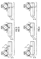
- FIGS. 3 and 4 are sequential, schematic views showing the mechanism during the printing stroke and the solder collected at the end of the wiping stroke of a squeegee blade in the art (FIG. 3) and a squeegee blade fabricated according to an embodiment of the invention (FIG. 4).
-
- Electroformed squeegee blades are used in the printing operation of the electronics packaging industry, and more particularly in surface mount manufacturing. Unlike conventional methods of producing squeegee blades, squeegee blades made according to the invention are grown atom by atom with an electroforming process that utilizes specialized chemistries and process conditions that render the squeegee blade with improved properties and characteristics related to the squeegee blade application.
- Print tests using the electroformed squeegee blade made according to the invention show a minimum 75% reduction in the amount of residual print material left on the stencil after each print cycle. The result is a reduction in the build-up of dzied material clogging stencil apertures and improved print definition. The enhanced printing consistency that results from the use of an electroformed squeegee blade made according to the invention reduces the occurrence of bridging, bleed-out and insufficient aperture filling, key causes of manufacturing defects. By reducing the number of defects associated with stencil printing, a reduction in manufacturing costs is achieved.
- Due to the enhanced material compatibility between the stencil and the electroformed squeegee blade, stencil wear normally associated with the printing operation is reduced. printing tests performed with current technology metal squeegee blades show stencil coining and wear by visual inspection, while electroformed squeegee blades exhibit little or no wear at all after an equal number of printing cycles on a test stencil.
- A major cause of the coining and wear seen for the current technology metal squeegee blades introduced during the manufacturing process is a lack of blade edge planarity. The electroformed squeegee blade fabricated according to the invention provides enhanced squeegee blade edge planarity that has been unachievable under current chemical etching, laser cutting, molding or secondary processing steps. As a result of the reduced wear, the life expectancy of the stencil is anticipated to increase by 200%. By increasing the number of print cycles due to decreased stencil wear, manufacturing quality remains consistent for an extended period of time, thus improving overall manufacturing yields. In comparative testing, after an egual number of print cycles with an electroformed versus a conventional metal squeegee blade, significant wear and coining can be observed with the conventional squeegee blade, while no wear can be detected with the electroformed squeegee blade.
- Another benefit of the electroformed squeegee blade fabricated according to the invention is that as the surface tension attributed to the squeegee blade is reduced, the tendency of the printing material to stick to the squeegee blade is minimized. This is a problem most noticeable during the use of two squeegee blades as the direction of squeegee blade travel is changed and a switch from front to rear or rear to front squeegee blades is made. The result is often a smearing of the printing material, presenting an opportunity for the introduction of printing defects. With an electroformed squeegee blade, the printing material has a tendency to roll into a uniform cylindrical mass ahead of the squeegee blade during printing. Because of the lowered surface tension associated with the electroformed squeegee blade, the cylindrical mass of printing material is left on the stencil, precisely aligned for the next print stroke. As a result, 30% less printing material is required to be applied to the stencil and waste is reduced. This more efficient use of printing material or solder paste reduces waste and improves the overall print deposition quality, uniformity and consistency.
- During printing trials, an electroformed squeegee blade made in accordance with the invention required a reduced amount of solder paste printing material relative to that of conventional squeegee blades. This is due to a minimization of sticking of the printing material to the squeegee blade, an elimination of accumulating or piling of printing material along the side of the stencil image outside of the squeegee's reach, and an overall cleaner stencil surface. In addition, improvement is achieved due to a consistent volume of paste being available across the whole stencil image area, which further enhances printing performance.
- The advantages of the invention extend beyond the actual printing process. After printing is completed and the clean-up process begins, a significant savings is realized in time, materials, and toxic material disposal costs. After each test printing run with an electroformed squeegee blade, clean-up has been reduced to less than 5 minutes, while printing with competitive squeegee blades including stainless steel, plated stainless steel, propriety specialty coated steel, and 80, 85 and 90 durometer polyurethane squeegee blades, requires anywhere from 15 to 30 minutes for clean-up. The number of clean-up wipes required after use of an electroformed squeegee blade is reduced to one from the fifteen to twenty required for competitive products. More efficient use of printing materials, reduced waste, and overall reduction in clean-up requirements, results in a dramatic reduction in toxic waste disposal costs.
- The method of the invention, which is a variation of the method disclosed in U.S. Patent No. 5,478,699 to Blessington deceased, et al., involves electrodepositing metal on a conductive substrate.
- Typical substrate materials include stainless steel, iron plated with chromium or nickel, nickel, copper, titanium, aluminum, aluminum plated with chromium or nickel, titanium palladium alloys, nickel-copper alloys such as Inconel® 600 and Invar® (available from Inco, Saddle Brook, New Jersey and the like. Non-metallic substrates can also be used if they have been made conductive, for example, by being appropriately metallized using metallization techniques known to the art, such as electroless metallization, vapor deposition, and the like. A conductive substrate is first cleaned by methods well known to those of skill in the art. The sequence of cleaning steps can include washing with isopropyl alcohol, vapor degreasing in trichloroethylene, electrocleaning, rinsing in distilled water, washing in nitric acid, and final rinsing in distilled water.
- The process takes place within an electroforming zone comprising an anode, a cathode, and an electroforming bath. The bath may be composed of: ions or salts of ions of the layer-forming material, the concentration of which can range from trace to saturation, which ions can be in the form of anions or cations; a solvent; a buffering agent, the concentration of which can range from zero to saturation; an anode corrosion agent, the concentration of which can range from zero to saturation; and, optionally, grain refiners, levelers, catalysts, surfactants, and other additives known in the art. The preferred concentration ranges may readily be established by those of skill in the art without undue experimentation.
- A preferred electroforming bath to plate nickel on a substrate comprises about 70-90 mg/ml of nickel ion in solution, about 20-40 mg/ml of H3BO3, about 3.0 mg/ml of NiCl2·6H2O and about 4.0-6.0 ml/liter of sodium lauryl sulfate. Other suitable electroforming bath compositions include, but are not limited to, Watts nickel: about 68-88 mg/ml of nickel ion, about 50-70 mg/ml of NiCl2·6H2O and about 20-40 mg/ml of H3BO3; chloride sulfate: about 70-100 mg/ml of nickel ion, about 145-170 mg/ml of NiCl2·6H2O and about 30-45 mg/ml H3BO3; and concentrated sulfamate: about 100-120 mg/ml of nickel ion, about 3-10 mg/ml of NiCl2·6H2O and about 30-45 mg/ml of H3BO3. Electroless baths such as electroless. nickel baths can also be employed. Various types are available depending upon the properties required in the electroform deposition. These electroless baths are well known to those skilled in the art.
- Examples of metals that can be electroformed onto the surface of a substrate include, but are not limited to, nickel, copper, gold, silver, palladium, tin, lead, chromium, zinc, cobalt, iron, and alloys thereof. Preferred metals are nickel and copper. Any suitable conductor or material that can be electrochemically deposited can be used, such as conductive polymers, plastics, and electroless nickel deposits. Examples of suitable autocatalytic electroless nickel deposits include, but are not limited to, nickel-phosphorus, nickel-boron, poly-alloys, such as copper-nickel phosphorus, nickel-polytetrafluoroethylene, composite coatings, and the like. Methods of preparing electroless nickel deposits employed within the scope of this invention are well known to those skilled in the art of electroforming.
- The electrolytic bath is energized using a suitable electrical source. Layer-forming ions from the solution are electroformed onto the conductive surface of the substrate. The process is allowed to proceed until a single layer has deposited on the substrate preferably ranging in thickness from about 0.200 to about 0.385mm. After the single layer of metal is electroformed onto the surface of the substrate, the substrate is removed from the solution.
- In addition, a squeegee blade having desired features can be prepared using a pattern of resist having a design complementary to the desired features in accordance with the process disclosed in U.S. Patent No. 5,478,699.
- Referring to FIGS. 2 and 3, the
electroformed squeegee blade 5 made according to the invention causes the solder paste 1 to be applied to a uniform vertical height in thestencil apertures 7 regardless of their orientation. As a result of the uniform deposition of the solder paste into each of theapertures 7, thesolder pads 8 are uniformly deposited on the printedwiring board 9 of FIG. 2. The printedwiring board 9 is. firmly held in place beneath thestencil 6 by, e.g., suction, tooling holes, adjustable mechanical fixturing or dedicated mechanical fixturing and after the deposition of the solder paste 1 is then released to the next operation in the printed wiring board manufacturing process. - As a result, the printed
wiring board 9 withsolder pads 8 produced according to the invention will more firmly hold surface mounted integrated circuits and/or components to the printedwiring board 9 for subsequent mounting and soldering flow operations. - Referring to FIGS. 3 and 4, 80, 85 and 90 durometer polyurethane squeegee blades have been used as comparison materials against the electroformed squeegee blade of the invention. As can be seen, the electroformed squeegee blade made according to the invention, which has an HK500 hardness preferably about 200 to 600, and more preferably of about 390 to 450, permits a more uniform deposition of solder paste on the printed wiring board. As a result, the number of printed wiring boards that must be reworked for solder pad faults and integrated circuit mountings is minimal.
- While this invention has been described in conjunction with specific embodiments thereof, it is evident that many alternatives, modifications and variations will be apparent to those skilled in the art. Accordingly, the preferred embodiments of the invention as set forth herein are intended to be illustrative, not limiting. Various changes may be made.
Claims (9)
- A method of making an electroformed squeegee blade (5) comprising: electroforming a layer of material onto a substrate to provide the electroformed squeegee blade.
- The method of claim 1, wherein said electroformed layer of material comprises material selected from the group consisting of nickel, copper, gold, silver, palladium, tin, lead, chromium, zinc, cobalt, iron, and alloys thereof.
- The method of claim 2, wherein said electroformed layer of material comprises material selected from the group consisting of nickel and copper.
- The method of claim 1, wherein said electroformed layer of material comprises at least one material selected from the group consisting of nickel-phosphorous, nickel-boron, copper-nickel phosphorous, nickel-polytetrafluoroethylene, and composites thereof.
- The method of claim 1, said method comprising providing a conductive substrate core patterned with photoresist in a form of the squeegee blade and electroforming said layer of material onto said conductive substrate core to provide the electroformed squeegee blade.
- The method of claim 5, wherein said conductive substrate is a conductive substrate core patterned with photoresist in a form of the squeegee blade and electroforming said layer of material onto said conductive substrate core to provide the electroformed squeegee blade.
- The method of claim 6, wherein said conductive substrate core is selected from the group consisting of stainless steel, iron plated with chromium, iron plated with nickel, nickel, copper, titanium, aluminum, aluminum plated with chromium, aluminum plated with nickel, titanium palladium alloys and nickel-copper alloys.
- A method for depositing a printing material (1) on a substrate (9) using a squeegee blade (5), said method comprising:characterized in thatplacing a stencil having a plurality of apertures (7) therethrough in contact with said substrate;depositing said printing material (1) onto said stencil; andmoving the squeegee blade (5) across said stencil to spread said printing material (1) across said stencil and deposit said printing material on said substrate,
the squeegee blade (5) is made with a method in accordance with claim 1. - The method of claim 8, wherein solder paste (1) is provided as the printing material and a printed wiring board (9) is provided as the substrate.
Applications Claiming Priority (3)
| Application Number | Priority Date | Filing Date | Title |
|---|---|---|---|
| US08/646,380 US5746127A (en) | 1996-05-03 | 1996-05-03 | Electroformed squeegee blade for surface mount screen printing |
| US646380 | 1996-05-03 | ||
| PCT/US1997/007630 WO1997041969A1 (en) | 1996-05-03 | 1997-05-05 | Electroformed squeegee blade for surface mount screen printing |
Publications (3)
| Publication Number | Publication Date |
|---|---|
| EP1015130A1 EP1015130A1 (en) | 2000-07-05 |
| EP1015130A4 EP1015130A4 (en) | 2000-07-05 |
| EP1015130B1 true EP1015130B1 (en) | 2002-11-20 |
Family
ID=24592816
Family Applications (1)
| Application Number | Title | Priority Date | Filing Date |
|---|---|---|---|
| EP97923561A Expired - Lifetime EP1015130B1 (en) | 1996-05-03 | 1997-05-05 | Electroforming method for making a squeegee blade |
Country Status (9)
| Country | Link |
|---|---|
| US (1) | US5746127A (en) |
| EP (1) | EP1015130B1 (en) |
| AT (1) | ATE228037T1 (en) |
| AU (1) | AU2933597A (en) |
| DE (1) | DE69717319T2 (en) |
| DK (1) | DK1015130T3 (en) |
| ES (1) | ES2187777T3 (en) |
| PT (1) | PT1015130E (en) |
| WO (1) | WO1997041969A1 (en) |
Families Citing this family (17)
| Publication number | Priority date | Publication date | Assignee | Title |
|---|---|---|---|---|
| FR2754474B1 (en) * | 1996-10-15 | 1999-04-30 | Novatec | DEVICE FOR DEPOSITING A VISCOUS OR PASTA ON A SUBSTRATE THROUGH THE OPENINGS OF A STENCIL |
| EP0848586B1 (en) * | 1996-12-10 | 2007-01-24 | Matsushita Electric Industrial Co., Ltd. | Apparatus and method for printing solder paste |
| US5947021A (en) * | 1997-11-04 | 1999-09-07 | Photo Stencil, Inc. | Metal squeegee blade with a titanium nitride coating |
| TW409490B (en) * | 1998-12-31 | 2000-10-21 | World Wiser Electronics Inc | The equipment for plug hole process and the method thereof |
| US6550662B2 (en) * | 2001-04-03 | 2003-04-22 | Kyocera Wireless Corporation | Chip rework solder tool |
| US6659002B2 (en) * | 2001-10-31 | 2003-12-09 | International Business Machines Corporation | Screening apparatus with trailing squeegee and method of screening |
| DE60312947T2 (en) * | 2002-09-24 | 2007-12-13 | Matsushita Electric Industrial Co., Ltd., Kadoma | PRESSURE PLATE, PCB AND METHOD FOR PRINTING A PCB |
| US7726239B2 (en) * | 2005-08-24 | 2010-06-01 | Seagate Technology Llc | Controlled deposition of printing material |
| US20070232055A1 (en) * | 2006-03-31 | 2007-10-04 | Richard Earl Corley | Methods and Apparatuses for Applying a Protective Material to an Interconnect Associated with a Component |
| US20130213247A1 (en) * | 2012-02-17 | 2013-08-22 | Samsung Electronics Co., Ltd. | Stencil apparatus for printing solder paste |
| CN103287063B (en) * | 2012-02-29 | 2015-11-18 | 三星电子株式会社 | For the stencil equipment of Printing Paste |
| JP6517216B2 (en) | 2013-12-31 | 2019-05-22 | ジョンソン・アンド・ジョンソン・コンシューマー・インコーポレイテッド | Single pass method for forming multilayer shaped film products |
| KR102396906B1 (en) | 2013-12-31 | 2022-05-13 | 존슨 앤드 존슨 컨수머 인코포레이티드 | Process for forming a multi layered shaped film |
| CN105873573B (en) | 2013-12-31 | 2020-11-24 | 强生消费者公司 | Method of forming a formed film product |
| JP6913248B2 (en) * | 2018-06-05 | 2021-08-04 | ヤマハ発動機株式会社 | Printing equipment |
| US10960607B2 (en) * | 2018-12-13 | 2021-03-30 | General Electric Company | Systems and methods for monitoring powder spreading in additive manufacturing systems |
| TWI698287B (en) * | 2019-08-27 | 2020-07-11 | 華碩電腦股份有限公司 | Method of coating liquid metal heat-dissipatng paste and heat-dissipatng module using liquid metal heat-dissipatng paste |
Family Cites Families (9)
| Publication number | Priority date | Publication date | Assignee | Title |
|---|---|---|---|---|
| US3930455A (en) * | 1974-09-19 | 1976-01-06 | Harry Bremer | Boat hull construction |
| JPH0288787A (en) * | 1988-09-27 | 1990-03-28 | Matsushita Electric Works Ltd | Electroformed blade |
| US5078082A (en) * | 1989-08-16 | 1992-01-07 | Smt East Corporation | Method and apparatus for applying bonding material to a populated mounting surface |
| US5044306A (en) * | 1990-06-11 | 1991-09-03 | Gunter Erdmann | Solder applying mechanism |
| JP3004416B2 (en) * | 1991-09-13 | 2000-01-31 | 理想科学工業株式会社 | Squeegee device for ink supply of stencil printing machine |
| JP3025361B2 (en) * | 1992-02-07 | 2000-03-27 | 理想科学工業株式会社 | Blade type squeegee device for stencil printing machine |
| US5478699A (en) * | 1992-03-12 | 1995-12-26 | Amtx, Inc. | Method for preparing a screen printing stencil |
| US5254362A (en) * | 1992-10-23 | 1993-10-19 | Motorola, Inc. | Method and apparatus for deposition of solder paste on a printed wiring board |
| US5387044A (en) * | 1993-12-15 | 1995-02-07 | Accardo; Thomas A. | Screen filler applicator for the screen printing industry |
-
1996
- 1996-05-03 US US08/646,380 patent/US5746127A/en not_active Expired - Lifetime
-
1997
- 1997-05-05 EP EP97923561A patent/EP1015130B1/en not_active Expired - Lifetime
- 1997-05-05 DE DE69717319T patent/DE69717319T2/en not_active Expired - Fee Related
- 1997-05-05 DK DK97923561T patent/DK1015130T3/en active
- 1997-05-05 WO PCT/US1997/007630 patent/WO1997041969A1/en not_active Ceased
- 1997-05-05 AU AU29335/97A patent/AU2933597A/en not_active Abandoned
- 1997-05-05 PT PT97923561T patent/PT1015130E/en unknown
- 1997-05-05 ES ES97923561T patent/ES2187777T3/en not_active Expired - Lifetime
- 1997-05-05 AT AT97923561T patent/ATE228037T1/en not_active IP Right Cessation
Also Published As
| Publication number | Publication date |
|---|---|
| DK1015130T3 (en) | 2003-03-17 |
| ATE228037T1 (en) | 2002-12-15 |
| AU2933597A (en) | 1997-11-26 |
| PT1015130E (en) | 2003-03-31 |
| EP1015130A1 (en) | 2000-07-05 |
| WO1997041969A1 (en) | 1997-11-13 |
| ES2187777T3 (en) | 2003-06-16 |
| DE69717319T2 (en) | 2003-04-03 |
| US5746127A (en) | 1998-05-05 |
| EP1015130A4 (en) | 2000-07-05 |
| DE69717319D1 (en) | 2003-01-02 |
Similar Documents
| Publication | Publication Date | Title |
|---|---|---|
| US5746127A (en) | Electroformed squeegee blade for surface mount screen printing | |
| US5359928A (en) | Method for preparing and using a screen printing stencil having raised edges | |
| CN1077040C (en) | Squeegee for screen printing and its production method | |
| US7469635B2 (en) | Method and apparatus for performing operations within a stencil printer | |
| US5984166A (en) | Process for creating fine and coarse pitch solder deposits on printed ciruit boards | |
| US5478699A (en) | Method for preparing a screen printing stencil | |
| KR100557549B1 (en) | Flip chip bump pad forming method and structure | |
| US5813331A (en) | Method of printing with a differential thickness stencil | |
| JP2006347165A (en) | Metal mask for making pattern | |
| US5947021A (en) | Metal squeegee blade with a titanium nitride coating | |
| JP3120130B2 (en) | Manufacturing method of metal mask plate for printing | |
| EP0784914B1 (en) | Method of manufacturing a printed circuit board | |
| US6398935B1 (en) | Method for manufacturing pcb's | |
| JP4186900B2 (en) | Circuit forming board manufacturing equipment | |
| JP6894141B2 (en) | Metal mask and its manufacturing method | |
| JPH0243356B2 (en) | ||
| JPH10323962A (en) | Method of manufacturing mesh-integrated metal mask | |
| JP4113906B2 (en) | Manufacturing method of mesh-integrated metal mask | |
| JPH09174809A (en) | Squeegee for screen printing | |
| JPH07276842A (en) | Metal mask | |
| Manessis et al. | Latest technological advancements in stencil printing processes for ultra-fine-pitch flip-chip bumping down to 60 mm pitch | |
| KR20090062793A (en) | Elastic printing master and its manufacturing method | |
| WO2000048845A1 (en) | Improved stencil | |
| JP3600340B2 (en) | Screen printing squeegee | |
| JP2020150136A (en) | Manufacturing method of conductive ball stationary mask |
Legal Events
| Date | Code | Title | Description |
|---|---|---|---|
| PUAI | Public reference made under article 153(3) epc to a published international application that has entered the european phase |
Free format text: ORIGINAL CODE: 0009012 |
|
| 17P | Request for examination filed |
Effective date: 19990301 |
|
| A4 | Supplementary search report drawn up and despatched |
Effective date: 19990611 |
|
| AK | Designated contracting states |
Kind code of ref document: A4 Designated state(s): AT BE CH DE DK ES FI FR GB GR IE IT LI LU MC NL PT SE Kind code of ref document: A1 Designated state(s): AT BE CH DE DK ES FI FR GB GR IE IT LI LU MC NL PT SE |
|
| 17Q | First examination report despatched |
Effective date: 20010612 |
|
| RTI1 | Title (correction) |
Free format text: ELECTROFORMING METHOD FOR MAKING A SQUEEGEE BLADE |
|
| GRAG | Despatch of communication of intention to grant |
Free format text: ORIGINAL CODE: EPIDOS AGRA |
|
| GRAG | Despatch of communication of intention to grant |
Free format text: ORIGINAL CODE: EPIDOS AGRA |
|
| GRAH | Despatch of communication of intention to grant a patent |
Free format text: ORIGINAL CODE: EPIDOS IGRA |
|
| GRAH | Despatch of communication of intention to grant a patent |
Free format text: ORIGINAL CODE: EPIDOS IGRA |
|
| GRAA | (expected) grant |
Free format text: ORIGINAL CODE: 0009210 |
|
| AK | Designated contracting states |
Kind code of ref document: B1 Designated state(s): AT BE CH DE DK ES FI FR GB GR IE IT LI LU MC NL PT SE |
|
| REF | Corresponds to: |
Ref document number: 228037 Country of ref document: AT Date of ref document: 20021215 Kind code of ref document: T |
|
| REG | Reference to a national code |
Ref country code: GB Ref legal event code: FG4D |
|
| REG | Reference to a national code |
Ref country code: CH Ref legal event code: NV Representative=s name: E. BLUM & CO. PATENTANWAELTE Ref country code: CH Ref legal event code: EP |
|
| REG | Reference to a national code |
Ref country code: IE Ref legal event code: FG4D |
|
| REF | Corresponds to: |
Ref document number: 69717319 Country of ref document: DE Date of ref document: 20030102 |
|
| REG | Reference to a national code |
Ref country code: DK Ref legal event code: T3 |
|
| REG | Reference to a national code |
Ref country code: GR Ref legal event code: EP Ref document number: 20030400397 Country of ref document: GR |
|
| REG | Reference to a national code |
Ref country code: PT Ref legal event code: SC4A Free format text: AVAILABILITY OF NATIONAL TRANSLATION Effective date: 20030120 |
|
| ET | Fr: translation filed | ||
| REG | Reference to a national code |
Ref country code: ES Ref legal event code: FG2A Ref document number: 2187777 Country of ref document: ES Kind code of ref document: T3 |
|
| PLBE | No opposition filed within time limit |
Free format text: ORIGINAL CODE: 0009261 |
|
| STAA | Information on the status of an ep patent application or granted ep patent |
Free format text: STATUS: NO OPPOSITION FILED WITHIN TIME LIMIT |
|
| 26N | No opposition filed |
Effective date: 20030821 |
|
| REG | Reference to a national code |
Ref country code: CH Ref legal event code: PFA Owner name: XEROX CORPORATION Free format text: XEROX CORPORATION#XEROX SQUARE - 20A#ROCHESTER, NEW YORK 14644 (US) -TRANSFER TO- XEROX CORPORATION#XEROX SQUARE - 20A#ROCHESTER, NEW YORK 14644 (US) |
|
| PGFP | Annual fee paid to national office [announced via postgrant information from national office to epo] |
Ref country code: LU Payment date: 20080606 Year of fee payment: 12 Ref country code: ES Payment date: 20080526 Year of fee payment: 12 Ref country code: DK Payment date: 20080528 Year of fee payment: 12 Ref country code: CH Payment date: 20080530 Year of fee payment: 12 |
|
| PGFP | Annual fee paid to national office [announced via postgrant information from national office to epo] |
Ref country code: AT Payment date: 20080421 Year of fee payment: 12 |
|
| PGFP | Annual fee paid to national office [announced via postgrant information from national office to epo] |
Ref country code: MC Payment date: 20080418 Year of fee payment: 12 Ref country code: PT Payment date: 20080421 Year of fee payment: 12 Ref country code: FI Payment date: 20080530 Year of fee payment: 12 |
|
| PGFP | Annual fee paid to national office [announced via postgrant information from national office to epo] |
Ref country code: SE Payment date: 20080529 Year of fee payment: 12 Ref country code: NL Payment date: 20080524 Year of fee payment: 12 Ref country code: IE Payment date: 20080528 Year of fee payment: 12 Ref country code: DE Payment date: 20080630 Year of fee payment: 12 |
|
| PGFP | Annual fee paid to national office [announced via postgrant information from national office to epo] |
Ref country code: IT Payment date: 20080528 Year of fee payment: 12 |
|
| PGFP | Annual fee paid to national office [announced via postgrant information from national office to epo] |
Ref country code: GR Payment date: 20080530 Year of fee payment: 12 |
|
| REG | Reference to a national code |
Ref country code: PT Ref legal event code: MM4A Free format text: LAPSE DUE TO NON-PAYMENT OF FEES Effective date: 20091105 |
|
| PG25 | Lapsed in a contracting state [announced via postgrant information from national office to epo] |
Ref country code: MC Free format text: LAPSE BECAUSE OF NON-PAYMENT OF DUE FEES Effective date: 20090531 |
|
| REG | Reference to a national code |
Ref country code: CH Ref legal event code: PL |
|
| REG | Reference to a national code |
Ref country code: DK Ref legal event code: EBP |
|
| PG25 | Lapsed in a contracting state [announced via postgrant information from national office to epo] |
Ref country code: LI Free format text: LAPSE BECAUSE OF NON-PAYMENT OF DUE FEES Effective date: 20090531 Ref country code: FI Free format text: LAPSE BECAUSE OF NON-PAYMENT OF DUE FEES Effective date: 20090505 Ref country code: CH Free format text: LAPSE BECAUSE OF NON-PAYMENT OF DUE FEES Effective date: 20090531 Ref country code: AT Free format text: LAPSE BECAUSE OF NON-PAYMENT OF DUE FEES Effective date: 20090505 |
|
| NLV4 | Nl: lapsed or anulled due to non-payment of the annual fee |
Effective date: 20091201 |
|
| PG25 | Lapsed in a contracting state [announced via postgrant information from national office to epo] |
Ref country code: NL Free format text: LAPSE BECAUSE OF NON-PAYMENT OF DUE FEES Effective date: 20091201 |
|
| REG | Reference to a national code |
Ref country code: FR Ref legal event code: ST Effective date: 20100129 |
|
| REG | Reference to a national code |
Ref country code: IE Ref legal event code: MM4A |
|
| PG25 | Lapsed in a contracting state [announced via postgrant information from national office to epo] |
Ref country code: PT Free format text: LAPSE BECAUSE OF NON-PAYMENT OF DUE FEES Effective date: 20091105 |
|
| PG25 | Lapsed in a contracting state [announced via postgrant information from national office to epo] |
Ref country code: IE Free format text: LAPSE BECAUSE OF NON-PAYMENT OF DUE FEES Effective date: 20090505 Ref country code: FR Free format text: LAPSE BECAUSE OF NON-PAYMENT OF DUE FEES Effective date: 20090602 Ref country code: DK Free format text: LAPSE BECAUSE OF NON-PAYMENT OF DUE FEES Effective date: 20090531 |
|
| PGFP | Annual fee paid to national office [announced via postgrant information from national office to epo] |
Ref country code: FR Payment date: 20080519 Year of fee payment: 12 |
|
| PG25 | Lapsed in a contracting state [announced via postgrant information from national office to epo] |
Ref country code: GR Free format text: LAPSE BECAUSE OF NON-PAYMENT OF DUE FEES Effective date: 20091202 Ref country code: DE Free format text: LAPSE BECAUSE OF NON-PAYMENT OF DUE FEES Effective date: 20091201 |
|
| REG | Reference to a national code |
Ref country code: ES Ref legal event code: FD2A Effective date: 20090506 |
|
| PG25 | Lapsed in a contracting state [announced via postgrant information from national office to epo] |
Ref country code: ES Free format text: LAPSE BECAUSE OF NON-PAYMENT OF DUE FEES Effective date: 20090506 |
|
| PG25 | Lapsed in a contracting state [announced via postgrant information from national office to epo] |
Ref country code: IT Free format text: LAPSE BECAUSE OF NON-PAYMENT OF DUE FEES Effective date: 20090505 |
|
| PG25 | Lapsed in a contracting state [announced via postgrant information from national office to epo] |
Ref country code: LU Free format text: LAPSE BECAUSE OF NON-PAYMENT OF DUE FEES Effective date: 20090505 |
|
| PG25 | Lapsed in a contracting state [announced via postgrant information from national office to epo] |
Ref country code: SE Free format text: LAPSE BECAUSE OF NON-PAYMENT OF DUE FEES Effective date: 20090506 |
|
| PGFP | Annual fee paid to national office [announced via postgrant information from national office to epo] |
Ref country code: BE Payment date: 20111028 Year of fee payment: 15 |
|
| PGFP | Annual fee paid to national office [announced via postgrant information from national office to epo] |
Ref country code: GB Payment date: 20120905 Year of fee payment: 16 |
|
| BERE | Be: lapsed |
Owner name: *XEROX CORP. Effective date: 20120531 |
|
| PG25 | Lapsed in a contracting state [announced via postgrant information from national office to epo] |
Ref country code: BE Free format text: LAPSE BECAUSE OF NON-PAYMENT OF DUE FEES Effective date: 20120531 |
|
| GBPC | Gb: european patent ceased through non-payment of renewal fee |
Effective date: 20130505 |
|
| PG25 | Lapsed in a contracting state [announced via postgrant information from national office to epo] |
Ref country code: GB Free format text: LAPSE BECAUSE OF NON-PAYMENT OF DUE FEES Effective date: 20130505 |