EP1006697A2 - Parellel signal processing for equalisation on fibre channels - Google Patents
Parellel signal processing for equalisation on fibre channels Download PDFInfo
- Publication number
- EP1006697A2 EP1006697A2 EP99309305A EP99309305A EP1006697A2 EP 1006697 A2 EP1006697 A2 EP 1006697A2 EP 99309305 A EP99309305 A EP 99309305A EP 99309305 A EP99309305 A EP 99309305A EP 1006697 A2 EP1006697 A2 EP 1006697A2
- Authority
- EP
- European Patent Office
- Prior art keywords
- signal
- channel
- adaptive
- equalizer
- clock rate
- Prior art date
- Legal status (The legal status is an assumption and is not a legal conclusion. Google has not performed a legal analysis and makes no representation as to the accuracy of the status listed.)
- Withdrawn
Links
Images
Classifications
-
- H—ELECTRICITY
- H03—ELECTRONIC CIRCUITRY
- H03M—CODING; DECODING; CODE CONVERSION IN GENERAL
- H03M1/00—Analogue/digital conversion; Digital/analogue conversion
- H03M1/06—Continuously compensating for, or preventing, undesired influence of physical parameters
- H03M1/0602—Continuously compensating for, or preventing, undesired influence of physical parameters of deviations from the desired transfer characteristic
- H03M1/0609—Continuously compensating for, or preventing, undesired influence of physical parameters of deviations from the desired transfer characteristic at two points of the transfer characteristic, i.e. by adjusting two reference values, e.g. offset and gain error
-
- H—ELECTRICITY
- H04—ELECTRIC COMMUNICATION TECHNIQUE
- H04L—TRANSMISSION OF DIGITAL INFORMATION, e.g. TELEGRAPHIC COMMUNICATION
- H04L25/00—Baseband systems
- H04L25/02—Details ; arrangements for supplying electrical power along data transmission lines
- H04L25/03—Shaping networks in transmitter or receiver, e.g. adaptive shaping networks
- H04L25/03006—Arrangements for removing intersymbol interference
- H04L25/03012—Arrangements for removing intersymbol interference operating in the time domain
-
- H—ELECTRICITY
- H03—ELECTRONIC CIRCUITRY
- H03M—CODING; DECODING; CODE CONVERSION IN GENERAL
- H03M1/00—Analogue/digital conversion; Digital/analogue conversion
- H03M1/12—Analogue/digital converters
- H03M1/1205—Multiplexed conversion systems
- H03M1/121—Interleaved, i.e. using multiple converters or converter parts for one channel
- H03M1/1215—Interleaved, i.e. using multiple converters or converter parts for one channel using time-division multiplexing
-
- H—ELECTRICITY
- H04—ELECTRIC COMMUNICATION TECHNIQUE
- H04L—TRANSMISSION OF DIGITAL INFORMATION, e.g. TELEGRAPHIC COMMUNICATION
- H04L25/00—Baseband systems
- H04L25/02—Details ; arrangements for supplying electrical power along data transmission lines
- H04L25/03—Shaping networks in transmitter or receiver, e.g. adaptive shaping networks
- H04L25/03006—Arrangements for removing intersymbol interference
- H04L2025/0335—Arrangements for removing intersymbol interference characterised by the type of transmission
- H04L2025/03356—Baseband transmission
-
- H—ELECTRICITY
- H04—ELECTRIC COMMUNICATION TECHNIQUE
- H04L—TRANSMISSION OF DIGITAL INFORMATION, e.g. TELEGRAPHIC COMMUNICATION
- H04L25/00—Baseband systems
- H04L25/02—Details ; arrangements for supplying electrical power along data transmission lines
- H04L25/03—Shaping networks in transmitter or receiver, e.g. adaptive shaping networks
- H04L25/03006—Arrangements for removing intersymbol interference
- H04L2025/03433—Arrangements for removing intersymbol interference characterised by equaliser structure
- H04L2025/03439—Fixed structures
- H04L2025/03445—Time domain
Definitions
- the present invention relates generally to channel equalization techniques, and more particularly, to channel equalization techniques for reducing dispersion problems in fiber channels.
- the transmission rates for local area networks have progressively increased from 10 Megabits-per-second (Mbps) using twisted pair conductors to 1 Gigabit-per-second (Gbps) using multi-mode fiber channels.
- LANs local area networks
- Gbps gigabit-per-second
- a result of delay spread in a multi-mode fiber channel is that it considerably reduces the distance over which digital data can be accurately transmitted.
- Typical fibers used for gigabit transmission have a cutoff frequency specification of 200 Megahertz kilometer (MHz-km). Thus, there is a trade-off between channel lengths and bandwidth.
- the cable length should be limited to approximately 200 meters.
- the Gigabit Ethernet standard operates at a bit rate of 1.25 Gigabits-per-second (GBps), has a corresponding bandwidth of 612.5 MHz and thus has a maximum channel length of 326.5 meters.
- the Gigabit Ethernet standard limits the maximum channel length to 275 meters,. It is desirable, however, to transmit digital signals on a fiber channel over distances of one kilometer or more.
- fiber channel lengths for high speed digital signals could be increased by implementing channel equalization techniques in the receiver, such as those channel equalization techniques applied to more non-fiber based channels, e.g., twisted pair conductors
- typical fiber receivers have not implemented any kind of sophisticated channel equalization. This is because of the practical difficulty of implementing a channel equalizer that operates at such high clock rates, e.g., on the order of one Gigahertz.
- a method and apparatus for reducing delay spread problems in data signals received over a channel, such as a fiber channel, by processing the received data on parallel branches at a rate that is slower than the original clock rate.
- the present invention makes channel equalization possible, despite the very high clock rates of the received signal.
- the original clock rate of the received signal is reduced by an arbitrary factor, N.
- the received signal is sampled and digitized using N parallel paths that are each triggered with a clock that is 1/N-times as fast as the original clock rate.
- the converted samples are processed using digital signal processing (DSP) techniques.
- DSP digital signal processing
- the incoming signal is sampled and digitized in parallel at a clock rate that is 1/N-times as fast as the incoming clock rate.
- the analog samples are digitized in parallel before digital signal processing (DSP) techniques are applied by an adaptive digital signal processor to perform data detection.
- DSP digital signal processing
- the adaptive digital signal processor may be embodied, for example, as an adaptive channel equalizer that utilizes an adaptive feed forward equalizer (FFE), as a combined adaptive feed forward equalizer (FFE) with a decision feedback equalizer (DFE), or as a maximum likelihood sequence estimator (MLSE), such as a Viterbi detector, combined with channel estimation.
- FFE adaptive feed forward equalizer
- FFE combined adaptive feed forward equalizer
- DFE decision feedback equalizer
- MBE maximum likelihood sequence estimator
- FIG. 1 illustrates a receiver 100 in accordance with the present invention that reduces dispersion problems in data signals received over a fiber channel 110.
- the receiver 100 processes different portions of the received data on parallel branches at a rate that is slower than the original clock rate.
- the present invention makes channel equalization possible for fiber channels despite the very high clock rates of the received signal and appears to perform channel equalization at the original clock rate.
- N trigger clocks, ⁇ 1 through ⁇ N are generated from the clock rate of the received signal.
- the clock rate of each of the trigger clocks, ⁇ 1 through ⁇ N is reduced by an arbitrary factor N for sampling and digitizing the analog signal at the output of the fiber channel 110, and then processing the converted samples using digital signal processing (DSP) techniques.
- DSP digital signal processing
- the bit rate is 1.25 Gigabits-per-second (Gbps)
- the signals can be sampled, digitized and processed using a 1/N-times as fast clock rate of 125 Megahertz (MHz).
- each bit can be processed for 8 nanoseconds, which is achievable with currently available technology.
- the energy of the received signal is increased by a preamplifier 115 before being sampled by a series of N track and hold circuits 120-1 through 120-N that are each triggered by a respective trigger clock, ⁇ 1 through ⁇ N , that is 1/N-times as fast as the incoming clock rate.
- the incoming clock, clk, associated with the received data, and the various 1/N-times slower clocks, ⁇ 1 through ⁇ N are shown in FIG. 2.
- the received data can be processed in parallel at a rate that is 1/N-times as fast as the incoming clock rate.
- the parallel analog samples are then converted to a digital signal by N analog-to-digital converters 130-1 through 130-N before digital signal processing (DSP) techniques are applied by an adaptive digital signal processor 140 in order to perform data detection, discussed below.
- DSP digital signal processing
- FIG. 3 illustrates one suitable implementation of the receiver 100 in accordance with the present invention.
- the analog data from the output of the preamplifier 115 (FIG. 1) is applied to N analog-to-digital converters 320-1 through 320-N that are each triggered by a respective trigger clock, ⁇ 1 through ⁇ N , that is 1/N-times as fast as the incoming clock rate.
- a digital phase locked loop (DPLL) 325 performs clock recovery of the incoming clock signal, clk, associated with the received data, and generates the various 1/N-times faster clocks, ⁇ 1 through ⁇ N .
- the received data is processed in parallel at a rate that is 1/N-times as fast as the incoming clock rate.
- the digital outputs of the analog-to-digital converters 320-1 through 320-N are stored in N registers 330-1 through 330-N that are all triggered by the same 1/N-times as fast digital clock to resynchronize the parallel branches.
- the receiver 100 optionally includes error estimation circuits 340-1 through 340-N, gain control circuits 350-1 through 350-N and offset cancellation circuits 360-1 through 360-N for each of the N parallel branches.
- error estimation circuit 340-k, gain control circuits 350-k and offset cancellation circuits 360-k are only shown in detail in FIG. 3 for the k-th branch of the receiver 100, corresponding error estimation circuits 340-1 through 340-N, gain control circuits 350-1 through 350-N and offset cancellation circuits 360-1 through 360-N would be included in each of the N parallel branches.
- a reference signal is applied, and the error estimation circuits 340-1 through 340-N measure the error and generate an error signal, e N .
- the error signal is generated by comparing the detected value, X, to a two level quantized value produced by a quantizer 370-1 through 370-N.
- the quantizer 370-1 through 370-N receives the value X, and generates an applied reference signal indicating the sign of X (having a value equal to positive or negative 1).
- the error signal, e N is 1.
- the error signal, e N is used to update the gain control circuits 350-1 through 350-N and offset cancellation circuits 360-1 through 360-N.
- the raw output of the analog-to-digital converter 320-k is D k
- the gain correction circuit 350-k produces a signal A k , that is gain error free.
- the corrected and calibrated digital data is referred to as X k .
- Each of the individual gain and offset errors are corrected since the incoming symbol on each path is random and cyclostationary (a random variable that periodically has the same statistical properties).
- the digital data, X k is operated on by an adaptive digital signal processor 370 that performs channel equalization and data detection to produce the output symbols or bits, b 1 though b n .
- the adaptive digital signal processor 370 may be embodied, for example, as an adaptive channel equalizer 500 or a maximum likelihood sequence estimator (MLSE) 650, such as a Viterbi detector.
- MSE maximum likelihood sequence estimator
- FIG. 4 illustrates one suitable implementation of a receiver 100 in accordance with the present invention.
- the receiver 100 includes an analog whitening matched filter (WMF) 410 that preprocesses the analog signal prior to digitization by an analog-to-digital (A/D) converter 420.
- the digitized data is then processed by an adaptive channel equalizer 500, discussed further below in conjunction with FIG. 5, that produces the output symbols or bits, b 1 though b n .
- the feedback loop includes a channel estimator 440 that determines appropriate tap weight values to perform clock recovery.
- the channel estimator 440 uses the decided symbols from the adaptive channel equalizer 500 to perform blind or decision-directed tap adaptation.
- the channel estimator 440 is discussed further below in a section entitled PARALLEL IMPLEMENTATION OF A CHANNEL EQUALIZER.
- the tap weights, h k determined by the channel estimator 440 are applied in the clock recovery loop by a phase detector 450 and a low pass filter 460 to select a clock phase and generate the 1/N clocks. Each time the tap weights, h k , are adjusted, a new clock phase is selected in the clock recovery loop.
- FIG. 5 illustrates the adaptive channel equalizer 500 of FIG. 4.
- the adaptive channel equalizer 500 includes an adaptive feed forward equalizer (FFE) 510 in parallel form, and a slicer 520 that quantizes the digital data.
- FFE adaptive feed forward equalizer
- An implementation of the adaptive feed forward equalizer (FFE) 510 is discussed further below in a section entitled PARALLEL IMPLEMENTATION OF A CHANNEL EQUALIZER.
- An error signal, e k is generated in the feedback loop by a summer 530 that adapt the taps of the adaptive feed forward equalizer (FFE) 510.
- DFE decision feedback equalizer
- DFEs parallel decision feedback equalizers
- FIG. 6 illustrates an alternate implementation of a receiver 100 in accordance with the present invention.
- the receiver 100 includes an analog whitening matched filter (WMF) 610 that preprocesses the analog signal prior to digitization by an analog-to-digital (A/D) converter 620.
- the digitized data is then processed by a maximum likelihood sequence estimator (MLSE) 650, such as a Viterbi detector, that performs data detection without equalization to produce the output symbols or bits, b 1 though b n .
- Maximum likelihood sequence estimators (MLSE) 650 consider a number of possible sequences and determines which sequence was actually received, in a known manner.
- the feedback loop includes a channel estimator 640 that determines appropriate tap weight values to perform maximum likelihood sequence estimation.
- the channel estimator 640 uses the decided symbols from the maximum likelihood sequence estimator (MLSE) 630 to perform blind or decision-directed tap adaptation.
- the channel estimator 640 is discussed further below in a section entitled PARALLEL IMPLEMENTATION OF A CHANNEL EQUALIZER.
- the tap weights, h k determined by the channel estimator 640 are applied in the clock recovery loop by a phase detector 650 and a low pass filter 660 to select a clock phase and generate the 1/N times as fast clocks. Each time the tap weights, h k , are adjusted, a new clock phase is selected in the clock recovery loop, in a known manner.
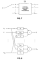
- FIG. 7 illustrates a schematic block diagram of a parallel channel equalizer.
- Let X represent the input of the channel equalizer 700 and Y the output, and (X 0 , X 1 , .... X N ) and (Y 0 , Y 1 , ... Y N ) the parallel representation of X and Y, respectively, where each of the X k or Y k values are clocked 1/N-times as fast as X and Y.
- X(z) X 0 (z) + z -1 X 1 (z) + ... + z -N+1 X N-1 (z)
- H(z) H 0 (z) + z -1 H 1 (z) + ... + z -N+1 H N-1 (z)
- H j and X j are given by: and m is the number of taps for the equalizer.
- Xj(Z) is the subsample at phase j of the input signal X, as shown in FIG. 7.
- FIG. 8 illustrates a parallel finite impulse response (FIR) filter 800 that implements Equation 6.
Landscapes
- Engineering & Computer Science (AREA)
- Theoretical Computer Science (AREA)
- Power Engineering (AREA)
- Computer Networks & Wireless Communication (AREA)
- Signal Processing (AREA)
- Dc Digital Transmission (AREA)
- Cable Transmission Systems, Equalization Of Radio And Reduction Of Echo (AREA)
Abstract
Description


Claims (14)
- A method for receiving a signal from a dispersible channel, said signal having an incoming clock rate, said method comprising the steps of:equalizing said channel using a plurality of parallel paths, each of said paths having a clock rate slower than said incoming clock rate; anddetecting said signal using a digital signal processor (DSP) that processes said signal using said parallel paths.
- The method according to claim 1, further comprising the step of sampling said signal on each of said plurality of parallel paths.
- The method according to claim 1, further comprising the step of digitizing said signal on each of said plurality of parallel paths.
- The method according to claim 2, wherein said sampling is performed using interleaved analog-to-digital converters.
- The method according to any of the preceding claims, wherein said equalizing step is performed using N parallel paths, each triggered by a clock that is 1/N-times as fast as said incoming clock rate.
- The method according to any of the preceding claims, wherein said equalizing and detecting steps are performed using an adaptive channel equalizer.
- The method according to claim 6, wherein said adapative channel equalizer includes an adaptive feed forward equalizer (FFE).
- The method according to claim 6, wherein the performance of said adaptive channel equalizer is improved using a decision feedback equalizer (DFE).
- The method according to any of claims 1 to 5, wherein said detecting step is performed using a maximum likelihood sequence estimator.
- The method according to claim 9, wherein said maximum likelihood sequence estimator is implemented as a Viterbi detector.
- A receiver adapted to receive a signal from a channel, said signal having an incoming clock rate, said receiver comprising means for carrying out each step of a method as claimed in any of the preceding claims.
- A method for calibrating an interleaved analog-to-digital converter to produce a calibrated output of said interleaved analog-to-digital converter, said method comprising the steps of:generating an error signal for each path of said interleaved analog-to-digital converter by comparing said calibrated output with a quantized version of said calibrated output; andadjusting a gain control circuit as a function of said error signal.
- A method for calibrating an interleaved analog-to-digital converter to produce a calibrated output of said interleaved analog-to-digital converter, said method comprising the steps of:generating an error signal for each path of said interleaved analog-to-digital converter by comparing said calibrated output with a quantized version of said calibrated output; andadjusting an offset correction circuit as a function of said error signal.
- The method according to claim 12 or claim 13, wherein said quantizer provides a two level signal indicating whether said calibrated output is higher or lower than an expected value.
Applications Claiming Priority (2)
| Application Number | Priority Date | Filing Date | Title |
|---|---|---|---|
| US203969 | 1988-06-08 | ||
| US20396998A | 1998-12-02 | 1998-12-02 |
Publications (2)
| Publication Number | Publication Date |
|---|---|
| EP1006697A2 true EP1006697A2 (en) | 2000-06-07 |
| EP1006697A3 EP1006697A3 (en) | 2004-01-02 |
Family
ID=22756035
Family Applications (1)
| Application Number | Title | Priority Date | Filing Date |
|---|---|---|---|
| EP99309305A Withdrawn EP1006697A3 (en) | 1998-12-02 | 1999-11-23 | Parellel signal processing for equalisation on fibre channels |
Country Status (1)
| Country | Link |
|---|---|
| EP (1) | EP1006697A3 (en) |
Cited By (21)
| Publication number | Priority date | Publication date | Assignee | Title |
|---|---|---|---|---|
| WO2002071713A2 (en) | 2001-03-01 | 2002-09-12 | Broadcom Corporation | Compensation of distortion due to channel and to receiver, in a parallel transmission system |
| WO2002071616A3 (en) * | 2001-03-01 | 2003-10-16 | Broadcom Corp | Methods and systems for dsp-based receivers |
| US6995594B2 (en) | 2000-04-28 | 2006-02-07 | Broadcom Corporation | Phase interpolator device and method |
| WO2007041601A2 (en) | 2005-10-03 | 2007-04-12 | Clariphy Communications, Inc. | Multi-channel equalization to compensate for impairments introduced by interleaved devices |
| US7245638B2 (en) | 2000-07-21 | 2007-07-17 | Broadcom Corporation | Methods and systems for DSP-based receivers |
| WO2007092067A2 (en) | 2005-11-15 | 2007-08-16 | Clariphy Communications, Inc. | High-speed receiver architecture |
| EP1892909A1 (en) | 2006-08-25 | 2008-02-27 | Broadcom Corporation | Electronic dispersion compensation utilizing interleaved architecture and channel identification for assisting timing recovery |
| US7525470B2 (en) | 2006-08-25 | 2009-04-28 | Broadcom Corporation | Phase control for interleaved analog-to-digital conversion for electronic dispersion compensation |
| US7525462B2 (en) | 2006-08-25 | 2009-04-28 | Broadcom Corporation | Gain control for interleaved analog-to-digital conversion for electronic dispersion compensation |
| US7560986B2 (en) | 2006-08-25 | 2009-07-14 | Broadcom Corporation | Variable gain amplifier and method for achieving variable gain amplification with high bandwidth and linearity |
| WO2009137007A3 (en) * | 2008-05-08 | 2010-03-04 | Altera Corporation | Digital equalizer for high-speed serial communications |
| US7933341B2 (en) * | 2000-02-28 | 2011-04-26 | Broadcom Corporation | System and method for high speed communications using digital signal processing |
| CN101179305B (en) * | 2006-08-25 | 2011-09-07 | 美国博通公司 | System and method for electronic dispersion compensation |
| US8094056B2 (en) | 2006-02-02 | 2012-01-10 | Clariphy Communications, Inc. | Analog-to-digital converter |
| US8139630B2 (en) | 2005-10-03 | 2012-03-20 | Clariphy Communications, Inc. | High-speed receiver architecture |
| US8300685B2 (en) | 2006-08-25 | 2012-10-30 | Broadcom Corporation | Non-linear decision feedback equalizer |
| US8483343B2 (en) | 2005-10-03 | 2013-07-09 | Clariphy Communications, Inc. | High-speed receiver architecture |
| US8750320B2 (en) | 1997-01-23 | 2014-06-10 | Broadcom Corporation | Fibre channel arbitrated loop bufferless switch circuitry to increase bandwidth without significant increase in cost |
| US8798091B2 (en) | 1998-11-19 | 2014-08-05 | Broadcom Corporation | Fibre channel arbitrated loop bufferless switch circuitry to increase bandwidth without significant increase in cost |
| US8831074B2 (en) | 2005-10-03 | 2014-09-09 | Clariphy Communications, Inc. | High-speed receiver architecture |
| US9160405B1 (en) | 2009-04-16 | 2015-10-13 | Altera Corporation | Self-tuning high speed transceiver for IC wireline channel |
Family Cites Families (6)
| Publication number | Priority date | Publication date | Assignee | Title |
|---|---|---|---|---|
| JPH065822B2 (en) * | 1989-01-19 | 1994-01-19 | 日本電気株式会社 | Parallel processing transversal equalizer |
| US5495501A (en) * | 1992-09-02 | 1996-02-27 | Fujitsu Limited | Communication system including a digital roll-off filter |
| DE4332735C2 (en) * | 1993-09-25 | 2002-04-04 | Bosch Gmbh Robert | Method for digitally generating a complex baseband signal |
| SE9501679D0 (en) * | 1995-05-05 | 1995-05-05 | Centek | Detector device |
| US6167082A (en) * | 1997-03-06 | 2000-12-26 | Level One Communications, Inc. | Adaptive equalizers and methods for carrying out equalization with a precoded transmitter |
| CA2201834A1 (en) * | 1997-04-04 | 1998-10-04 | Gennum Corporation | Serial digital data communications receiver with improved automatic cable equalizer, agc system, and dc restorer |
-
1999
- 1999-11-23 EP EP99309305A patent/EP1006697A3/en not_active Withdrawn
Cited By (51)
| Publication number | Priority date | Publication date | Assignee | Title |
|---|---|---|---|---|
| US8750320B2 (en) | 1997-01-23 | 2014-06-10 | Broadcom Corporation | Fibre channel arbitrated loop bufferless switch circuitry to increase bandwidth without significant increase in cost |
| US8774199B2 (en) | 1997-01-23 | 2014-07-08 | Broadcom Corporation | Fibre channel arbitrated loop bufferless switch circuitry to increase bandwidth without significant increase in cost |
| US8767756B2 (en) | 1997-01-23 | 2014-07-01 | Broadcom Corporation | Fibre channel arbitrated loop bufferless switch circuitry to increase bandwidth without significant increase in cost |
| US8798091B2 (en) | 1998-11-19 | 2014-08-05 | Broadcom Corporation | Fibre channel arbitrated loop bufferless switch circuitry to increase bandwidth without significant increase in cost |
| US7933341B2 (en) * | 2000-02-28 | 2011-04-26 | Broadcom Corporation | System and method for high speed communications using digital signal processing |
| US6995594B2 (en) | 2000-04-28 | 2006-02-07 | Broadcom Corporation | Phase interpolator device and method |
| US7058150B2 (en) | 2000-04-28 | 2006-06-06 | Broadcom Corporation | High-speed serial data transceiver and related methods |
| US7016449B2 (en) | 2000-04-28 | 2006-03-21 | Broadcom Corporation | Timing recovery and frequency tracking system and method |
| US8223828B2 (en) | 2000-04-28 | 2012-07-17 | Broadcom Corporation | Methods and systems for adaptive receiver equalization |
| US7012983B2 (en) | 2000-04-28 | 2006-03-14 | Broadcom Corporation | Timing recovery and phase tracking system and method |
| US7286597B2 (en) | 2000-04-28 | 2007-10-23 | Broadcom Corporation | Methods and systems for adaptive receiver equalization |
| US8824538B2 (en) | 2000-04-28 | 2014-09-02 | Broadcom Corporation | Methods and systems for adaptive receiver equalization |
| US8433020B2 (en) | 2000-04-28 | 2013-04-30 | Broadcom Corporation | High-speed serial data transceiver and related methods |
| US8472512B2 (en) | 2000-04-28 | 2013-06-25 | Broadcom Corporation | Methods and systems for adaptive receiver equalization |
| US8798219B2 (en) | 2000-04-28 | 2014-08-05 | Broadcom Corporation | High-speed serial data transceiver and related methods |
| US7564866B2 (en) * | 2000-07-21 | 2009-07-21 | Broadcom Corporation | Methods and systems for digitally processing optical data signals |
| US7778286B2 (en) | 2000-07-21 | 2010-08-17 | Broadcom Corporation | Methods and systems for DSP-based receivers |
| US8363683B2 (en) | 2000-07-21 | 2013-01-29 | Broadcom Corporation | Methods and systems for DSP-based receivers |
| US7245638B2 (en) | 2000-07-21 | 2007-07-17 | Broadcom Corporation | Methods and systems for DSP-based receivers |
| US7835387B2 (en) | 2000-07-21 | 2010-11-16 | Broadcom Corporation | Methods and systems for digitally processing data signals |
| WO2002071713A2 (en) | 2001-03-01 | 2002-09-12 | Broadcom Corporation | Compensation of distortion due to channel and to receiver, in a parallel transmission system |
| US7336729B2 (en) | 2001-03-01 | 2008-02-26 | Broadcom Corporation | Digital signal processing based de-serializer |
| WO2002071713A3 (en) * | 2001-03-01 | 2003-05-01 | Broadcom Corp | Compensation of distortion due to channel and to receiver, in a parallel transmission system |
| WO2002071616A3 (en) * | 2001-03-01 | 2003-10-16 | Broadcom Corp | Methods and systems for dsp-based receivers |
| US10841013B2 (en) | 2005-10-03 | 2020-11-17 | Inphi Corporation | High-speed receiver architecture |
| US10505638B2 (en) | 2005-10-03 | 2019-12-10 | Inphi Corporation | High-speed receiver architecture |
| US8483343B2 (en) | 2005-10-03 | 2013-07-09 | Clariphy Communications, Inc. | High-speed receiver architecture |
| US9882648B2 (en) | 2005-10-03 | 2018-01-30 | Inphi Corporation | High-speed receiver architecture |
| US8139630B2 (en) | 2005-10-03 | 2012-03-20 | Clariphy Communications, Inc. | High-speed receiver architecture |
| US9531475B2 (en) | 2005-10-03 | 2016-12-27 | Clariphy Communications, Inc. | High-speed receiver architecture |
| US8265134B2 (en) | 2005-10-03 | 2012-09-11 | Clariphy Communications, Inc. | Multi-channel equalization to compensate for impairments introduced by interleaved devices |
| WO2007041601A2 (en) | 2005-10-03 | 2007-04-12 | Clariphy Communications, Inc. | Multi-channel equalization to compensate for impairments introduced by interleaved devices |
| US8831074B2 (en) | 2005-10-03 | 2014-09-09 | Clariphy Communications, Inc. | High-speed receiver architecture |
| EP1941690A4 (en) * | 2005-10-03 | 2011-06-08 | Clariphy Comm Inc | MULTICANAL EQUALIZATION TO COMPENSATE THE WEAKNESSES INTRODUCED BY INTERLACED DEVICES |
| US10097273B2 (en) | 2005-10-03 | 2018-10-09 | Inphi Corporation | High-speed receiver architecture |
| EP1972054A4 (en) * | 2005-11-15 | 2011-06-08 | Clariphy Comm Inc | HIGH SPEED RECEIVER ARCHITECTURE |
| WO2007092067A2 (en) | 2005-11-15 | 2007-08-16 | Clariphy Communications, Inc. | High-speed receiver architecture |
| US8094056B2 (en) | 2006-02-02 | 2012-01-10 | Clariphy Communications, Inc. | Analog-to-digital converter |
| US7525462B2 (en) | 2006-08-25 | 2009-04-28 | Broadcom Corporation | Gain control for interleaved analog-to-digital conversion for electronic dispersion compensation |
| US8300685B2 (en) | 2006-08-25 | 2012-10-30 | Broadcom Corporation | Non-linear decision feedback equalizer |
| CN101179305B (en) * | 2006-08-25 | 2011-09-07 | 美国博通公司 | System and method for electronic dispersion compensation |
| US7961781B2 (en) | 2006-08-25 | 2011-06-14 | Broadcom Corporation | Electronic dispersion compensation utilizing interleaved architecture and channel identification for assisting timing recovery |
| US7755426B2 (en) | 2006-08-25 | 2010-07-13 | Broadcom Corporation | Variable gain amplifier and method for achieving variable gain amplification with high bandwidth and linearity |
| KR100912046B1 (en) | 2006-08-25 | 2009-08-12 | 브로드콤 코포레이션 | Electronic dispersion compensation utilizing interleaved architecture and channel identification for assisting timing recovery |
| EP1892909A1 (en) | 2006-08-25 | 2008-02-27 | Broadcom Corporation | Electronic dispersion compensation utilizing interleaved architecture and channel identification for assisting timing recovery |
| US7525470B2 (en) | 2006-08-25 | 2009-04-28 | Broadcom Corporation | Phase control for interleaved analog-to-digital conversion for electronic dispersion compensation |
| US7560986B2 (en) | 2006-08-25 | 2009-07-14 | Broadcom Corporation | Variable gain amplifier and method for achieving variable gain amplification with high bandwidth and linearity |
| WO2009137007A3 (en) * | 2008-05-08 | 2010-03-04 | Altera Corporation | Digital equalizer for high-speed serial communications |
| CN102089992B (en) * | 2008-05-08 | 2014-12-10 | 阿尔特拉公司 | Digital equalizer for high-speed serial communications |
| US8654898B2 (en) | 2008-05-08 | 2014-02-18 | Altera Corporation | Digital equalizer for high-speed serial communications |
| US9160405B1 (en) | 2009-04-16 | 2015-10-13 | Altera Corporation | Self-tuning high speed transceiver for IC wireline channel |
Also Published As
| Publication number | Publication date |
|---|---|
| EP1006697A3 (en) | 2004-01-02 |
Similar Documents
| Publication | Publication Date | Title |
|---|---|---|
| EP1006697A2 (en) | Parellel signal processing for equalisation on fibre channels | |
| KR100318801B1 (en) | Detector system having an equalizer | |
| US8472512B2 (en) | Methods and systems for adaptive receiver equalization | |
| US9071479B2 (en) | High-speed parallel decision feedback equalizer | |
| US8743945B2 (en) | Shift register based downsampled floating tap decision feedback equalization | |
| US8301036B2 (en) | High-speed adaptive decision feedback equalizer | |
| CN113472708B (en) | Eye monitor for parallel digital equalizer | |
| US7339990B2 (en) | Processing a received signal at a detection circuit | |
| EP1938537B1 (en) | Data communication circuit with equalization control | |
| US9935800B1 (en) | Reduced complexity precomputation for decision feedback equalizer | |
| US9215107B1 (en) | Dual loop clock and data recovery | |
| CN110858824B (en) | Pre-compensator based quantization for clock recovery | |
| US6618436B2 (en) | Digital base-band receiver | |
| EP1089484A2 (en) | Method and apparatus for fast burst mode data recovery | |
| CN112187683B (en) | Apparatus and method for parallel mixed signal equalization for high speed serial links | |
| US10833895B2 (en) | Receiver with selectable digital equalization filter options | |
| US11570024B2 (en) | Equalizer with perturbation effect based adaptation | |
| US8432960B2 (en) | Digital adaptive channel equalizer | |
| CN109873778A (en) | Linear feedback is balanced | |
| US11231740B2 (en) | Clock recovery using between-interval timing error estimation | |
| WO2005067236A1 (en) | Feedback filter | |
| US20050111559A1 (en) | Selection of pre-computed equalizer based on channel characteristic | |
| US20250150312A1 (en) | Serdes with robust parameter initialization |
Legal Events
| Date | Code | Title | Description |
|---|---|---|---|
| PUAI | Public reference made under article 153(3) epc to a published international application that has entered the european phase |
Free format text: ORIGINAL CODE: 0009012 |
|
| AK | Designated contracting states |
Kind code of ref document: A2 Designated state(s): AT BE CH CY DE DK ES FI FR GB GR IE IT LI LU MC NL PT SE |
|
| AX | Request for extension of the european patent |
Free format text: AL;LT;LV;MK;RO;SI |
|
| PUAL | Search report despatched |
Free format text: ORIGINAL CODE: 0009013 |
|
| RIC1 | Information provided on ipc code assigned before grant |
Ipc: 7H 04L 25/06 B Ipc: 7H 04L 25/03 A |
|
| AK | Designated contracting states |
Kind code of ref document: A3 Designated state(s): AT BE CH CY DE DK ES FI FR GB GR IE IT LI LU MC NL PT SE |
|
| AX | Request for extension of the european patent |
Extension state: AL LT LV MK RO SI |
|
| 17P | Request for examination filed |
Effective date: 20040326 |
|
| AKX | Designation fees paid |
Designated state(s): DE FR GB |
|
| STAA | Information on the status of an ep patent application or granted ep patent |
Free format text: STATUS: THE APPLICATION IS DEEMED TO BE WITHDRAWN |
|
| 18D | Application deemed to be withdrawn |
Effective date: 20060811 |