EP1005259A3 - Circuit board - Google Patents
Circuit board Download PDFInfo
- Publication number
- EP1005259A3 EP1005259A3 EP99123344A EP99123344A EP1005259A3 EP 1005259 A3 EP1005259 A3 EP 1005259A3 EP 99123344 A EP99123344 A EP 99123344A EP 99123344 A EP99123344 A EP 99123344A EP 1005259 A3 EP1005259 A3 EP 1005259A3
- Authority
- EP
- European Patent Office
- Prior art keywords
- metallic material
- circuit board
- electrically conductive
- considerably higher
- ohmic resistance
- Prior art date
- Legal status (The legal status is an assumption and is not a legal conclusion. Google has not performed a legal analysis and makes no representation as to the accuracy of the status listed.)
- Withdrawn
Links
- 239000007769 metal material Substances 0.000 abstract 3
- 239000004020 conductor Substances 0.000 abstract 1
Classifications
-
- H—ELECTRICITY
- H05—ELECTRIC TECHNIQUES NOT OTHERWISE PROVIDED FOR
- H05K—PRINTED CIRCUITS; CASINGS OR CONSTRUCTIONAL DETAILS OF ELECTRIC APPARATUS; MANUFACTURE OF ASSEMBLAGES OF ELECTRICAL COMPONENTS
- H05K1/00—Printed circuits
- H05K1/02—Details
- H05K1/0213—Electrical arrangements not otherwise provided for
- H05K1/0216—Reduction of cross-talk, noise or electromagnetic interference
- H05K1/0218—Reduction of cross-talk, noise or electromagnetic interference by printed shielding conductors, ground planes or power plane
- H05K1/0224—Patterned shielding planes, ground planes or power planes
-
- H—ELECTRICITY
- H05—ELECTRIC TECHNIQUES NOT OTHERWISE PROVIDED FOR
- H05K—PRINTED CIRCUITS; CASINGS OR CONSTRUCTIONAL DETAILS OF ELECTRIC APPARATUS; MANUFACTURE OF ASSEMBLAGES OF ELECTRICAL COMPONENTS
- H05K1/00—Printed circuits
- H05K1/02—Details
- H05K1/0213—Electrical arrangements not otherwise provided for
- H05K1/0216—Reduction of cross-talk, noise or electromagnetic interference
- H05K1/023—Reduction of cross-talk, noise or electromagnetic interference using auxiliary mounted passive components or auxiliary substances
- H05K1/0234—Resistors or by disposing resistive or lossy substances in or near power planes
-
- H—ELECTRICITY
- H05—ELECTRIC TECHNIQUES NOT OTHERWISE PROVIDED FOR
- H05K—PRINTED CIRCUITS; CASINGS OR CONSTRUCTIONAL DETAILS OF ELECTRIC APPARATUS; MANUFACTURE OF ASSEMBLAGES OF ELECTRICAL COMPONENTS
- H05K1/00—Printed circuits
- H05K1/16—Printed circuits incorporating printed electric components, e.g. printed resistor, capacitor, inductor
- H05K1/167—Printed circuits incorporating printed electric components, e.g. printed resistor, capacitor, inductor incorporating printed resistors
-
- H—ELECTRICITY
- H05—ELECTRIC TECHNIQUES NOT OTHERWISE PROVIDED FOR
- H05K—PRINTED CIRCUITS; CASINGS OR CONSTRUCTIONAL DETAILS OF ELECTRIC APPARATUS; MANUFACTURE OF ASSEMBLAGES OF ELECTRICAL COMPONENTS
- H05K1/00—Printed circuits
- H05K1/02—Details
- H05K1/0213—Electrical arrangements not otherwise provided for
- H05K1/0216—Reduction of cross-talk, noise or electromagnetic interference
- H05K1/023—Reduction of cross-talk, noise or electromagnetic interference using auxiliary mounted passive components or auxiliary substances
-
- H—ELECTRICITY
- H05—ELECTRIC TECHNIQUES NOT OTHERWISE PROVIDED FOR
- H05K—PRINTED CIRCUITS; CASINGS OR CONSTRUCTIONAL DETAILS OF ELECTRIC APPARATUS; MANUFACTURE OF ASSEMBLAGES OF ELECTRICAL COMPONENTS
- H05K2201/00—Indexing scheme relating to printed circuits covered by H05K1/00
- H05K2201/09—Shape and layout
- H05K2201/09209—Shape and layout details of conductors
- H05K2201/0929—Conductive planes
- H05K2201/093—Layout of power planes, ground planes or power supply conductors, e.g. having special clearance holes therein
-
- H—ELECTRICITY
- H05—ELECTRIC TECHNIQUES NOT OTHERWISE PROVIDED FOR
- H05K—PRINTED CIRCUITS; CASINGS OR CONSTRUCTIONAL DETAILS OF ELECTRIC APPARATUS; MANUFACTURE OF ASSEMBLAGES OF ELECTRICAL COMPONENTS
- H05K2201/00—Indexing scheme relating to printed circuits covered by H05K1/00
- H05K2201/09—Shape and layout
- H05K2201/09209—Shape and layout details of conductors
- H05K2201/09654—Shape and layout details of conductors covering at least two types of conductors provided for in H05K2201/09218 - H05K2201/095
- H05K2201/09681—Mesh conductors, e.g. as a ground plane
Landscapes
- Engineering & Computer Science (AREA)
- Microelectronics & Electronic Packaging (AREA)
- Physics & Mathematics (AREA)
- Electromagnetism (AREA)
- Parts Printed On Printed Circuit Boards (AREA)
- Structure Of Printed Boards (AREA)
- Shielding Devices Or Components To Electric Or Magnetic Fields (AREA)
Abstract
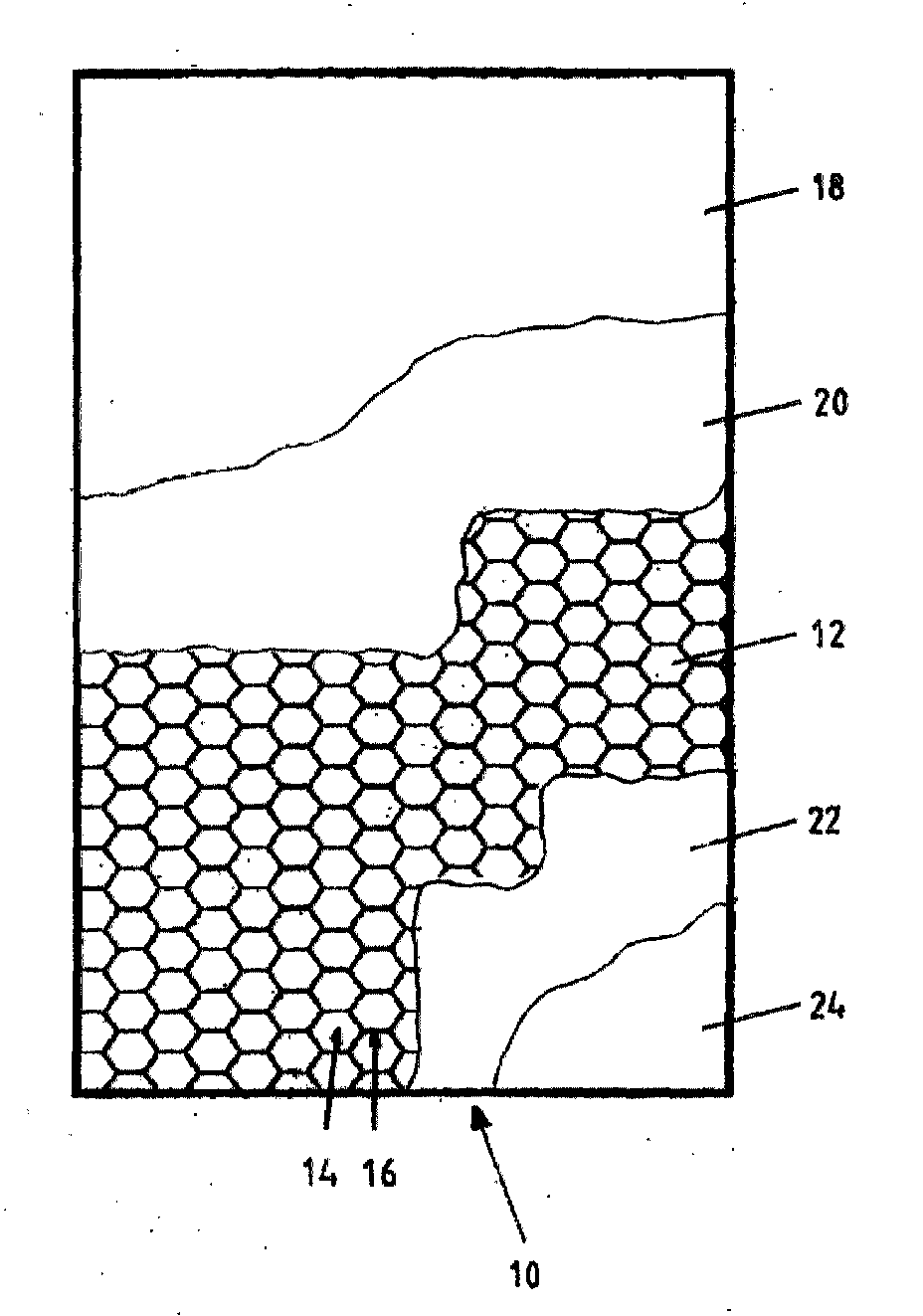
Die Leiterplatte (10) besitzt wenigstens eine elektrisch leitende
Fläche (12), die metallisches Material umfaßt.
Die Fläche ist in eine Vielzahl segmente (14) unterteilt, die durch
schmale Spalte (16) gegenseitig voneinander getrennt sind. Die Spalte
(16) sind mit einem elektrisch leitenden Material ausgefüllt, dessen
spezifischer ohmscher Widerstand wesentlich höher als der des
metallischen Materials ist. Demzufolge weist die Fläche (12) einen
mittleren Gesamtwiderstand auf, der erheblich höher ist als der ohmsche
Widerstand einer gleich großen einteiligen Fläche aus demselben
metallischen Material.
Applications Claiming Priority (2)
| Application Number | Priority Date | Filing Date | Title |
|---|---|---|---|
| DE1998154271 DE19854271A1 (en) | 1998-11-25 | 1998-11-25 | Circuit board |
| DE19854271 | 1998-11-25 |
Publications (2)
| Publication Number | Publication Date |
|---|---|
| EP1005259A2 EP1005259A2 (en) | 2000-05-31 |
| EP1005259A3 true EP1005259A3 (en) | 2002-02-20 |
Family
ID=7888903
Family Applications (1)
| Application Number | Title | Priority Date | Filing Date |
|---|---|---|---|
| EP99123344A Withdrawn EP1005259A3 (en) | 1998-11-25 | 1999-11-23 | Circuit board |
Country Status (2)
| Country | Link |
|---|---|
| EP (1) | EP1005259A3 (en) |
| DE (1) | DE19854271A1 (en) |
Families Citing this family (2)
| Publication number | Priority date | Publication date | Assignee | Title |
|---|---|---|---|---|
| AU2002308354A1 (en) * | 2001-03-08 | 2002-09-24 | Ilfa Industrieelektronik Und Leiterplattenfertigung Aller Art Gmbh | Multilayer printed circuit board |
| DE10336290A1 (en) * | 2003-08-07 | 2005-03-17 | Fraunhofer-Gesellschaft zur Förderung der angewandten Forschung e.V. | Circuit board for highest clocking frequencies, which includes a supply layer, also has damping structure attenuating waves more strongly at edges than in center |
Citations (4)
| Publication number | Priority date | Publication date | Assignee | Title |
|---|---|---|---|---|
| US5095407A (en) * | 1987-02-27 | 1992-03-10 | Hitachi, Ltd. | Double-sided memory board |
| JPH05198900A (en) * | 1992-01-23 | 1993-08-06 | Furukawa Electric Co Ltd:The | High frequency high current circuit board |
| DE4217425A1 (en) * | 1992-05-27 | 1993-12-02 | Deutsche Aerospace | Assembly carrier used to construct electronic circuits - comprising conducting pathways of resistance material to electrically connect individual electrical assemblies to carrier |
| US5364705A (en) * | 1992-06-25 | 1994-11-15 | Mcdonnell Douglas Helicopter Co. | Hybrid resistance cards and methods for manufacturing same |
-
1998
- 1998-11-25 DE DE1998154271 patent/DE19854271A1/en not_active Withdrawn
-
1999
- 1999-11-23 EP EP99123344A patent/EP1005259A3/en not_active Withdrawn
Patent Citations (4)
| Publication number | Priority date | Publication date | Assignee | Title |
|---|---|---|---|---|
| US5095407A (en) * | 1987-02-27 | 1992-03-10 | Hitachi, Ltd. | Double-sided memory board |
| JPH05198900A (en) * | 1992-01-23 | 1993-08-06 | Furukawa Electric Co Ltd:The | High frequency high current circuit board |
| DE4217425A1 (en) * | 1992-05-27 | 1993-12-02 | Deutsche Aerospace | Assembly carrier used to construct electronic circuits - comprising conducting pathways of resistance material to electrically connect individual electrical assemblies to carrier |
| US5364705A (en) * | 1992-06-25 | 1994-11-15 | Mcdonnell Douglas Helicopter Co. | Hybrid resistance cards and methods for manufacturing same |
Non-Patent Citations (2)
| Title |
|---|
| "KOHLENSTOFF STATT GOLD", ELEKTRONIK, FRANZIS VERLAG GMBH. MUNCHEN, DE, no. 1, 7 January 1997 (1997-01-07), pages 18 - 19, XP000685719, ISSN: 0013-5658 * |
| PATENT ABSTRACTS OF JAPAN vol. 017, no. 629 (E - 1462) 19 November 1993 (1993-11-19) * |
Also Published As
| Publication number | Publication date |
|---|---|
| DE19854271A1 (en) | 2000-05-31 |
| EP1005259A2 (en) | 2000-05-31 |
Similar Documents
| Publication | Publication Date | Title |
|---|---|---|
| DE2648979B2 (en) | Light emitting display device | |
| EP1233232A3 (en) | Lighting device | |
| EP0921609A3 (en) | Right angled HF coaxial connector | |
| DE3529218A1 (en) | CONNECTING DEVICE FOR CIRCUIT BOARDS | |
| DE3406093A1 (en) | PROBE FOR A ROBOT GRIPPER OR SIMILAR | |
| EP1338451A3 (en) | Electrical air heater, in particular for a motor vehicle | |
| DE102008024480A1 (en) | Electrical component arrangement | |
| EP1324063A3 (en) | Magnetoresistive sensor | |
| DE102009019285A1 (en) | Lighting system with at least one light strip | |
| EP0981177A3 (en) | Transmitting- and receiving device | |
| WO2002074025A3 (en) | Multilayer printed circuit board | |
| DE2943108A1 (en) | KEY SWITCH FOR PCB | |
| DE102008024481A1 (en) | Electrical component arrangement | |
| EP1096242A3 (en) | Pressure sensor | |
| DE60025301T2 (en) | Pushbutton Switches | |
| DE69839204T2 (en) | Conductive elastomer for grafting onto an elastic substrate | |
| EP1005259A3 (en) | Circuit board | |
| EP1079672A3 (en) | Plastic article comprising electrical contacts | |
| DE20309223U1 (en) | Basis for electronic components | |
| EP0867974A3 (en) | Electrical Contact element | |
| DE1276159B (en) | Stopper plate with an insulating base and process for its manufacture | |
| DE2523361C3 (en) | Electrical connector and method of making the same | |
| EP0829897A3 (en) | Electric fuse | |
| DE2929574A1 (en) | Flexible metallised sandwich key-pad - has flexible press-button cover with convoluted metallised underside held above baseplate contacts by insulator | |
| DE3336130A1 (en) | ELECTRIC SWITCH |
Legal Events
| Date | Code | Title | Description |
|---|---|---|---|
| PUAI | Public reference made under article 153(3) epc to a published international application that has entered the european phase |
Free format text: ORIGINAL CODE: 0009012 |
|
| AK | Designated contracting states |
Kind code of ref document: A2 Designated state(s): AT BE CH CY DE DK ES FI FR GB GR IE IT LI LU MC NL PT SE |
|
| AX | Request for extension of the european patent |
Free format text: AL;LT;LV;MK;RO;SI |
|
| PUAL | Search report despatched |
Free format text: ORIGINAL CODE: 0009013 |
|
| AK | Designated contracting states |
Kind code of ref document: A3 Designated state(s): AT BE CH CY DE DK ES FI FR GB GR IE IT LI LU MC NL PT SE |
|
| AX | Request for extension of the european patent |
Free format text: AL;LT;LV;MK;RO;SI |
|
| 17P | Request for examination filed |
Effective date: 20020412 |
|
| AKX | Designation fees paid |
Free format text: AT BE CH CY DE DK ES FI FR GB GR IE IT LI LU MC NL PT SE |
|
| 17Q | First examination report despatched |
Effective date: 20041028 |
|
| GRAP | Despatch of communication of intention to grant a patent |
Free format text: ORIGINAL CODE: EPIDOSNIGR1 |
|
| STAA | Information on the status of an ep patent application or granted ep patent |
Free format text: STATUS: THE APPLICATION IS DEEMED TO BE WITHDRAWN |
|
| 18D | Application deemed to be withdrawn |
Effective date: 20060601 |