EP1005159B1 - Switching circuit - Google Patents
Switching circuit Download PDFInfo
- Publication number
- EP1005159B1 EP1005159B1 EP99410104A EP99410104A EP1005159B1 EP 1005159 B1 EP1005159 B1 EP 1005159B1 EP 99410104 A EP99410104 A EP 99410104A EP 99410104 A EP99410104 A EP 99410104A EP 1005159 B1 EP1005159 B1 EP 1005159B1
- Authority
- EP
- European Patent Office
- Prior art keywords
- type
- region
- doped
- heavily
- metallization
- Prior art date
- Legal status (The legal status is an assumption and is not a legal conclusion. Google has not performed a legal analysis and makes no representation as to the accuracy of the status listed.)
- Expired - Lifetime
Links
Images

Classifications
-
- H—ELECTRICITY
- H03—ELECTRONIC CIRCUITRY
- H03K—PULSE TECHNIQUE
- H03K17/00—Electronic switching or gating, i.e. not by contact-making and –breaking
- H03K17/16—Modifications for eliminating interference voltages or currents
-
- H—ELECTRICITY
- H03—ELECTRONIC CIRCUITRY
- H03K—PULSE TECHNIQUE
- H03K17/00—Electronic switching or gating, i.e. not by contact-making and –breaking
- H03K17/51—Electronic switching or gating, i.e. not by contact-making and –breaking characterised by the components used
- H03K17/56—Electronic switching or gating, i.e. not by contact-making and –breaking characterised by the components used by the use, as active elements, of semiconductor devices
- H03K17/72—Electronic switching or gating, i.e. not by contact-making and –breaking characterised by the components used by the use, as active elements, of semiconductor devices having more than two PN junctions; having more than three electrodes; having more than one electrode connected to the same conductivity region
- H03K17/73—Electronic switching or gating, i.e. not by contact-making and –breaking characterised by the components used by the use, as active elements, of semiconductor devices having more than two PN junctions; having more than three electrodes; having more than one electrode connected to the same conductivity region for dc voltages or currents
- H03K17/732—Measures for enabling turn-off
Definitions
- the present invention as defined in the independent claims, relates generally to the field of switches and more particularly the realization of switches adapted to switch a circuit connected to the sector in a manner compatible with current standards relating to electromagnetic interference.
- thyristor-type switches that are normally open (which must be controlled to close) or mountings that are normally closed (which must be controlled to open) are commonly used.
- the control, on closing or opening, of these switches causes a strong variation of the current during a very short time interval. This sudden variation is likely to cause electromagnetic disturbances in neighboring equipment.
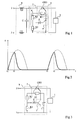
- FIG. 1 illustrates an example of a normally closed switch arrangement.
- a load 1 intended to receive a portion of the power that can provide an AC supply voltage source Vac, for example the mains voltage, applied between two terminals 2, 3.
- the power supplied to the load 1 is controlled by a switching circuit 4.
- the circuit 4 comprises a switch 5 and a control circuit 6.
- the switch 5 is a thyristor trigger (GTO), provided with anode and cathode triggers which are connected by a resistor R1.
- GTO thyristor trigger
- Figure 2 shows the shape of the current I in the load as a function of time. Thanks to the presence of the resistor R1, the GTO thyristor closes naturally at the beginning of each positive half-cycle of the voltage Vac (times t1).
- the purpose of the circuit 6 is to cause the thyristor GTO to open when the supply voltage Vac reaches a predetermined level.
- the circuit 6 comprises a reference diode or avalanche diode Z whose cathode is connected to the midpoint of a resistor bridge R2, R3.
- the values of the resistors R2, R3 are chosen so that the diode Z goes into avalanche when the voltage Vac reaches the level at which it is desired to interrupt the supply of the load 1.
- a switch 7 for example a thyristor, which closes when the diode Z becomes conducting, after which the switch 5 opens (times t2) and the current in the load drops sharply to zero, as shown in Figure 2 in dotted lines. Then, the current remains zero until the beginning of the next positive alternation where this sequence is repeated.
- a low-pass filter 8 is conventionally provided between each of the terminals 2, 3 and the circuit 4.
- the filter 8 comprises, for example, inductors L1 and L2 and a capacitor C.
- a first end of each of the inductors L1 , L2 is connected to one of the respective terminals 2, 3.
- the second ends of the inductors L1 and L2 are connected by the capacitor C and are respectively connected to the terminals of the series circuit comprising the GTO thyristor and the load 1.
- the values of inductances L1, L2 are typically of the order of 150 ⁇ H, and capacitance of capacitor C is typically 470 nF.
- a disadvantage of this type of conventional solution is that such a filter 8 is bulky, not integrable and expensive.
- US Patent 3899713 discloses a circuit comprising a switch (102, Fig. 2) which may be a cathode gate thyristor (104) (108). This thyristor is described only as an example of switches. Its gate open thyristor (GTO) function is not used. In particular, this patent describes columns 13 and 14 that the switch 102 is normally open.
- a switch 102, Fig. 2
- GTO gate open thyristor
- the present invention aims to propose a new switching circuit that can be used without a filter.
- the present invention also aims at providing such a switching circuit which is, for the most part, feasible in the form of a monolithic component.
- the present invention provides a type switching circuit comprising a trigger operable thyristor polarized to be normally closed, further comprising, between the trigger and a power line, a capacitor and a controllable switch connected in parallel.
- controllable switch is a bipolar transistor.
- the anode and cathode gates of the thyristor are interconnected via a resistor.
- a control terminal of the switch is connected to the anode of a reference diode whose cathode is connected to the midpoint of a resistor bridge.
- the present invention also provides a bidirectional switching circuit consisting of the antiparallel combination of two switching circuits according to any one of the preceding embodiments.
- the present invention also provides a switching circuit made in monolithic form in a semiconductor substrate of a first conductivity type having first and second zones delimited by first and second isolation walls, the first zone comprising the thyristor realized in form. lateral, its cathode gate being connected to the first wall, and comprising the resistor bridge; the second zone comprising the switch and the diode, the switch being a bipolar transistor formed vertically; and the rear face of the first zone being coated with an insulating layer leaving free at least part of the rear face of the first wall, a metallization covering the entire rear face and providing with the first insulation wall a connection between the cathode gate of the thyristor and the collector of the transistor.
- the second zone comprises on the side of the upper face a N-type channel stop ring heavily doped at the periphery of the box, the ring being covered with a metallization.
- the present invention also provides a switching circuit made in monolithic form in a semiconductor substrate of a first conductivity type having first and second zones delimited by isolation walls; the first zone comprising the thyristor realized in lateral form and the bridge of resistances; the second zone comprising the switch and the diode, the switch being a bipolar transistor formed laterally; the connection between the cathode gate of the thyristor and the collector of the transistor being provided on the side of the front face.
- the present invention provides for controlling the current decay at the moment of opening a normally conductive switch.
- Figure 3 illustrates an embodiment of the present invention. It is sought to limit across a load 1 the power supplied by a source of supply voltage Vac, for example the mains voltage of 220 volts, delivered between terminals 2 and 3. To do this, a circuit of switching 9 according to the present invention.
- a source of supply voltage Vac for example the mains voltage of 220 volts
- the circuit 9 comprises, like the circuit 4 of FIG. 1, a switch 5, a resistor R1, a reference diode Z and a resistor bridge R2, R3 mounted like the elements of the same references of FIG.
- the thyristor 7 is replaced by a bipolar transistor T and the circuit 9 further comprises, in parallel with the transistor T, a capacitor C '.
- the operation of the switching circuit according to the invention will appear more clearly hereinafter.
- the values of the different components are, for example, for a switched current of 1 A in a load of 50 ⁇ , a Z diode with a threshold of 10 V, a resistor R2 of 90 k ⁇ , a resistor R3 of 240 k ⁇ and a capacitor C 'with a capacitance of 22 nF.
- the switch 5 closes in the same way as in the circuit 4 of FIG. 1.
- the line current I is identical in this first phase. to that of the classic circuit.
- the capacitor C ' according to FIG. The invention discharges through the collector of the transistor T. As long as the transistor T is not saturated, this discharge is sinusoidal. Indeed, the collector current of the transistor T follows its base current which is a function of the voltage (sinusoidal) of the sector. Once the transistor T is saturated, this discharge is exponentially until the capacitor is completely discharged. Then, the current is canceled and the switch 5 is completely open. The transistor T remains saturated until the end of the positive half cycle, which keeps the switch 5 locked.
- An advantage of the present invention is therefore that the opening of the switch 5 is progressive and is accompanied by a relatively slow variation of the line current, as illustrated in FIG. 2, thus significantly limiting the electromagnetic disturbances on the neighboring equipment.
- FIG. 4 is a diagrammatic sectional view showing a first example of embodiment in monolithic form of the circuit of FIG. 3.
- the switching circuit 9 is made in monolithic form, with the exception of the capacitor C ', in a semiconductor substrate 10, for example made of silicon, of a first type of conductivity, for example N.
- this substrate are delimited a first zone surrounded by an isolation wall 11 and a second zone surrounded by an isolation wall 12.
- these zones are adjacent and a portion of the wall of Isolation 11 thus merges with a portion of the isolation wall 12.
- this isolation wall is made by deep diffusion of a dopant P from both sides of the substrate.
- a first P + type region 14 corresponds to the anode, the substrate 10 to the anode gate, the region 16 to the cathode gate and the region 18 to the cathode.
- the cathode will have a small width and a great length.
- a weakly doped P-type region 20 is formed in contact with the P + region 18, a second contact of which is formed by a another P + type region 22, itself short-circuited with an N + type region 24 formed in the substrate 10.
- lightly doped P-type regions 26 and 28 for example in the form of strips, which form the resistors R2 and R3, are also formed on the side of the upper face.
- the ends of these strips are integral with highly doped P-type regions 29, 30 and 31.
- the resistance R2 is formed, for example, between the regions 29 and 30 and the resistor R3 between the regions 30 and 31.
- the anode region 14 is coated with a metallization M1 and the cathode region 18 is coated with a metallization M2.
- a metallization M3 establishes the short-circuit between the P 22 and N 24 regions.
- the link between the anode gate of the GTO thyristor and a terminal of the resistor R2 is provided by a metallization M4 which connects the P-type region 29 to a highly doped N-type zone 33 formed in the substrate which, as previously seen, corresponds to the anode gate of the lateral thyristor GTO.
- the midpoint of resistors R2 and R3 is connected to a metallization M5 and the second terminal of the resistor R3 is connected to a metallization M6.
- the NPN transistor T and the avalanche diode Z are formed on the side of the upper face.
- a P-type box 41 has been formed in which regions of FIG. type N 42 and 43.
- the NPN transistor T is thus obtained whose emitter corresponds to the region 42, the base to the region 41 and the collector to the substrate 10 and to the N-type region 44.
- the diode Z corresponds to the junction between the N region 43 and the well P 41.
- a metallization M8 formed on the region 42 corresponds to the emitter of the transistor and a metallization M9 formed on the region 43 corresponds to the cathode of the diode Z.
- the metallization M8 is connected to the metallization M6 previously described. and to the ground while the metallization M9 is connected to the metallization M5 previously described.
- the metallizations M6 and M8 will preferably constitute one and the same metallization, as well as the metallizations M5 and M9.
- the isolation wall 11 is used. This isolation wall 11 is connected to the region 16. the embodiment shown, this connection is provided by continuity between the insulation wall and this region 16. It could also provide disjoint regions connected by a metallization.
- an insulating layer 51 is deposited opposite the first zone. This insulating layer leaves free at least part of the rear face of the wall 11.
- a metallization M10 covers the entire rear face and thus provides the aforementioned connection function.
- the monolithic embodiment described above does not include the capacitor VS'. It may be connected by a first terminal to the ground terminal connected to the metallization M8 and the second terminal to the backside metallization M10. It will also be possible to provide a metallization M14 formed on the side of the upper face of the substrate on the isolation walls and to which the second terminal of the capacitor will be connected.
- the metallization M10 has the sole function of ensuring the connection between the cathode gate of the thyristor GTO and collector of the transistor T and is not intended to be connected to an external terminal. It will simply serve to mount the component as is the case for many power components to be connected to a radiator.
- FIG. 4 is susceptible to various variations and modifications which will be apparent to those skilled in the art who can provide the various elements with conventional modifications to improve their functions or to provide additional functions.
- the structure shown in FIG. 4 can constitute the whole of a monolithic component or constitute a part of a larger monolithic component of which other elements would extend in the substrate 10 outside the parts represented and delimited by the insulating walls 11 and 12.
- FIG. 4 shows the formation of a heavily doped N-type ring from the upper surface. of the substrate having a channel stop function. This ring is designated by the reference 53 and may be coated with a metallization M12.
- FIG. 5 illustrates a second embodiment in monolithic form of the circuit of FIG. 3.
- the resistor bridge R2, R3, the resistor R1 and the thyristor GTO are formed in the same way as that described above in relation to FIG. 5.
- the region 16 constituting the cathode gate of the GTO thyristor is now separated from the isolation wall 11. It will then be possible to provide a channel stop region N '54 between the region 16 and the wall 11. It is then formed above the region 16 M7 metallization.
- the NPN type bipolar transistor T is formed laterally. Its base and its emitter, as well as the diode Z, are formed in the same way as that described above in relation to FIG. 4.
- the collector of the transistor T now corresponds to the ring N + 53 formed at the periphery of the subwoofer. base 41. M12 collector metallization is then provided on this ring 53.
- an insulating layer 55 is deposited on the side of the rear face of the substrate 10.
- An M11 metallization covers all of the rear face except possibly the rear face of the insulation walls and has the function of being used for mounting the component as is the case for many power components intended to be connected to a radiator.
- the monolithic embodiment described above does not include the capacitor C '. This will be connected between the ground terminal connected to the metallization M8 and the metallization M12.
- An advantage of this second embodiment is to completely isolate the two zones formed in the substrate, which avoids the appearance of additional parasitic junctions.
- An advantage of the present invention is that the switching circuit (9, Figure 3) is integrable, if not the capacitor C '( Figure 3).
- the capacitor C ' has a relatively small size.
- the filter conventionally used (8, FIG. 1) made use of two very bulky inductors (L1, L2) and a capacitor (C)
- the circuit according to the invention only uses one capacitor. (C 'in Figure 3) whose capacity is much lower than that of the capacitor of a conventional filter.
- the capacitor C is a filtering component whose value is calculated as a function of the inductances L1 and L2 but also as a function of the desired insertion loss (or attenuation).
- the capacitor C ' is not a filtering component but is used as a voltage generator controlled by the transistor T.
- the unidirectional circuit according to the present invention described previously with reference to FIGS. 2 to 6 may advantageously be used to produce a bidirectional switch capable of switching a circuit connected to the mains in a manner compatible with the current standards relating to electromagnetic disturbances.
- two unidirectional switches according to the present invention will be used, connected antiparallelly between two load supply terminals, in a manner that will be apparent to those skilled in the art.
- the resistor R2 may be an adjustable resistor, to allow dimmer applications or to adapt the threshold value of opening of the GTO thyristor.
- the exemplary switch in the form of a bipolar transistor (T) may be any of a variety of controllable linear closing switches known in the art.
Description
La présente invention telle que définie dans les revendications indépendante, concerne de façon genérale le domaine des commutateurs et plus particulièrement la réalisation de commutateurs propres à commuter un circuit connecté au secteur d'une façon compatible avec les normes actuelles relatives aux perturbations électromagnétiques.The present invention as defined in the independent claims, relates generally to the field of switches and more particularly the realization of switches adapted to switch a circuit connected to the sector in a manner compatible with current standards relating to electromagnetic interference.
Pour commuter une tension secteur élevée, on utilise couramment des commutateurs de type thyristor qui sont normalement ouverts (qui doivent être commandés pour se fermer) ou des montages qui sont normalement fermés (qui doivent être commandés pour s'ouvrir). La commande, à la fermeture ou à l'ouverture, de ces commutateurs entraîne une forte variation du courant pendant un intervalle de temps très bref. Cette variation brutale est susceptible de provoquer des perturbations électromagnétiques au niveau d'équipements voisins.To switch a high mains voltage, thyristor-type switches that are normally open (which must be controlled to close) or mountings that are normally closed (which must be controlled to open) are commonly used. The control, on closing or opening, of these switches causes a strong variation of the current during a very short time interval. This sudden variation is likely to cause electromagnetic disturbances in neighboring equipment.
La figure 1 illustre un exemple de montage à commutateur normalement fermé. On cherche ici à commander l'alimentation d'une charge 1 destinée à recevoir une partie de la puissance que peut fournir une source de tension d'alimentation alternative Vac, par exemple la tension du secteur, appliquée entre deux bornes 2, 3. La puissance fournie à la charge 1 est commandée par un circuit de commutation 4. Le circuit 4 comprend un commutateur 5 et un circuit de commande 6. Le commutateur 5 est un thyristor ouvrable par la gâchette (GTO), muni de gâchettes d'anode et de cathode qui sont connectées par une résistance R1.Figure 1 illustrates an example of a normally closed switch arrangement. We seek here to control the supply of a
La figure 2 représente l'allure du courant I dans la charge en fonction du temps. Grâce à la présence de la résistance R1, le thyristor GTO se ferme naturellement au début de chaque alternance positive de la tension Vac (instants tl). Le circuit 6 a pour objet de provoquer l'ouverture du thyristor GTO lorsque la tension d'alimentation Vac atteint un niveau prédéterminé. Dans l'exemple de réalisation illustré, le circuit 6 comprend une diode de référence ou diode à avalanche Z dont la cathode est connectée au point milieu d'un pont de résistances R2, R3. Les valeurs des résistances R2, R3 sont choisies pour que la diode Z passe en avalanche lorsque la tension Vac atteint le niveau auquel on souhaite interrompre l'alimentation de la charge 1. Entre la gâchette de cathode du thyristor GTO et la borne 3, est connecté un interrupteur 7, par exemple un thyristor, qui se ferme quand la diode Z devient passante, à la suite de quoi le commutateur 5 s'ouvre (instants t2) et le courant dans la charge chute brusquement à zéro, comme cela est illustré en figure 2 en pointillés. Ensuite, le courant demeure nul jusqu'au début de l'alternance positive suivante où cette séquence se répète.Figure 2 shows the shape of the current I in the load as a function of time. Thanks to the presence of the resistor R1, the GTO thyristor closes naturally at the beginning of each positive half-cycle of the voltage Vac (times t1). The purpose of the circuit 6 is to cause the thyristor GTO to open when the supply voltage Vac reaches a predetermined level. In the exemplary embodiment illustrated, the circuit 6 comprises a reference diode or avalanche diode Z whose cathode is connected to the midpoint of a resistor bridge R2, R3. The values of the resistors R2, R3 are chosen so that the diode Z goes into avalanche when the voltage Vac reaches the level at which it is desired to interrupt the supply of the
Comme cela a été mentionné précédemment, la variation brusque du courant sur la ligne d'alimentation aux instants t2 peut provoquer des perturbations électromagnétiques.As mentioned previously, the sudden change in current on the supply line at times t2 can cause electromagnetic disturbances.
Pour résoudre ce problème, on prévoit classiquement entre chacune des bornes 2, 3 et le circuit 4 un filtre passe-bas 8. Le filtre 8 comprend par exemple des inductances L1 et L2 et un condensateur C. Une première extrémité de chacune des inductances L1, L2 est connectée à une des bornes respectives 2, 3. Les secondes extrémités des inductances L1 et L2 sont connectées par le condensateur C et sont reliées respectivement aux bornes du circuit série comprenant le thyristor GTO et la charge 1. Pour un courant commuté de 1 A, les valeurs des inductances L1, L2 sont typiquement de l'ordre de 150 µH, et la capacité du condensateur C est typiquement de 470 nF. Un inconvénient de ce type de solution classique est qu'un tel filtre 8 est encombrant, non intégrable et cher.To solve this problem, a low-pass filter 8 is conventionally provided between each of the terminals 2, 3 and the circuit 4. The filter 8 comprises, for example, inductors L1 and L2 and a capacitor C. A first end of each of the inductors L1 , L2 is connected to one of the respective terminals 2, 3. The second ends of the inductors L1 and L2 are connected by the capacitor C and are respectively connected to the terminals of the series circuit comprising the GTO thyristor and the
Le brevet américain 3899713 décrit un circuit comprenant un commutateur (102, figure 2) qui peut être un thyristor (104) à gâchette de cathode (108). Ce thyristor est décrit uniquement à titre d'exemple de commutateurs. Sa fonction de thyristor ouvrable par la gâchette (GTO) n'est pas utilisée. En particulier, ce brevet décrit colonnes 13 et 14 que le commutateur 102 est normalement ouvert.US Patent 3899713 discloses a circuit comprising a switch (102, Fig. 2) which may be a cathode gate thyristor (104) (108). This thyristor is described only as an example of switches. Its gate open thyristor (GTO) function is not used. In particular, this patent describes
La présente invention vise à proposer un nouveau circuit de commutation qui puisse être utilisé sans filtre.The present invention aims to propose a new switching circuit that can be used without a filter.
La présente invention vise également à proposer un tel circuit de commutation qui soit, pour l'essentiel, réalisable sous forme d'un composant monolithique.The present invention also aims at providing such a switching circuit which is, for the most part, feasible in the form of a monolithic component.
Pour atteindre ces objets, la présente invention prévoit un circuit de commutation de type comprenant un thyristor ouvrable par la gâchette polarisé de façon à être normalement fermé, comportant en outre, entre la gâchette et une ligne d'alimentation, un condensateur et un commutateur commandable connectés en parallèle.To achieve these objects, the present invention provides a type switching circuit comprising a trigger operable thyristor polarized to be normally closed, further comprising, between the trigger and a power line, a capacitor and a controllable switch connected in parallel.
Selon un mode de réalisation de la présente invention, le commutateur commandable est un transistor bipolaire.According to one embodiment of the present invention, the controllable switch is a bipolar transistor.
Selon un mode de réalisation de la présente invention, les gâchettes d'anode et de cathode du thyristor sont interconnectées par l'intermédiaire d'une résistance.According to one embodiment of the present invention, the anode and cathode gates of the thyristor are interconnected via a resistor.
Selon un mode de réalisation de la présente invention, une borne de commande du commutateur est connectée à l'anode d'une diode de référence dont la cathode est connectée au point milieu d'un pont de résistances.According to an embodiment of the present invention, a control terminal of the switch is connected to the anode of a reference diode whose cathode is connected to the midpoint of a resistor bridge.
La présente invention prévoit également un circuit de commutation bidirectionnel constitué de l'association en antiparallèle de deux circuits de commutation selon l'un quelconque des modes de réalisation précédents.The present invention also provides a bidirectional switching circuit consisting of the antiparallel combination of two switching circuits according to any one of the preceding embodiments.
La présente invention prévoit également un circuit de commutation réalisé sous forme monolithique dans un substrat semiconducteur d'un premier type de conductivité comportant des première et seconde zones délimitées par des premier et second murs d'isolement, la première zone comprenant le thyristor réalisé sous forme latérale, sa gâchette de cathode étant connectée au premier mur, et comprenant le pont de résistances ; la deuxième zone comprenant le commutateur et la diode, le commutateur étant un transistor bipolaire formé verticalement ; et la face arrière de la première zone étant revêtue d'une couche isolante laissant libre une partie au moins de la face arrière du premier mur, une métallisation recouvrant l'ensemble de la face arrière et assurant avec le premier mur d'isolement une connexion entre la gâchette de cathode du thyristor et le collecteur du transistor.The present invention also provides a switching circuit made in monolithic form in a semiconductor substrate of a first conductivity type having first and second zones delimited by first and second isolation walls, the first zone comprising the thyristor realized in form. lateral, its cathode gate being connected to the first wall, and comprising the resistor bridge; the second zone comprising the switch and the diode, the switch being a bipolar transistor formed vertically; and the rear face of the first zone being coated with an insulating layer leaving free at least part of the rear face of the first wall, a metallization covering the entire rear face and providing with the first insulation wall a connection between the cathode gate of the thyristor and the collector of the transistor.
Selon un mode de réalisation de la présente invention, le circuit de commutation réalisé sous forme monolithique comprend du côté de la face supérieure du substrat, de type N :
- dans la première zone :
- une première région d'anode de type P fortement dopée recouverte d'une première métallisation ;
- une deuxième région de cathode de type N fortement dopée recouverte d'une deuxième métallisation ;
- une troisième région de type N fortement dopée, revêtue d'une troisième métallisation et en contact avec le substrat, correspondant à la gâchette d'anode ;
- une quatrième région de gâchette de cathode de type P fortement dopée, en contact avec le premier mur d'isolement ;
- une cinquième région de type P fortement dopée, en court-circuit, par la troisième métallisation, avec la troisième région, et en contact avec une sixième région de type P faiblement dopée, la sixième région étant en outre en contact avec la quatrième région et constituant une résistance entre les gâchettes d'anode et de cathode ;
- des régions de type P faiblement dopées, dont les extrémités sont solidaires de régions de type P fortement dopées revêtues de métallisations respectives, une des métallisations court-circuitant une région de type P, correspondant à une des résistances du pont de résistances, et une région de type N fortement dopée ; et
- dans la seconde région :
- un caisson de type P faiblement dopé, constituant la base du transistor, dans lequel sont formées des régions de type N fortement dopées, recouvertes de métallisations respectives, correspondant à l'émetteur du transistor et à la cathode de la diode ; et
- du côté de la face arrière du substrat, une région de type N fortement dopée constituant le collecteur du transistor.
- in the first zone:
- a first heavily doped P-type anode region covered with a first metallization;
- a second heavily doped N-type cathode region coated with a second metallization;
- a third heavily doped N-type region, coated with a third metallization and in contact with the substrate, corresponding to the anode gate;
- a fourth heavily doped P-type cathode gate region in contact with the first isolation wall;
- a fifth heavily doped P-type region short-circuited by the third metallization with the third region and in contact with a sixth lightly doped P-type region, the sixth region further being in contact with the fourth region; forming a resistance between the anode and cathode triggers;
- weakly doped P-type regions, the ends of which are integral with highly doped P-type regions coated with respective metallizations, one of the metallizations bypassing a P-type region, corresponding to one of the resistors of the resistance bridge, and a region strongly doped N-type; and
- in the second region:
- a lightly doped P-type well, constituting the base of the transistor, in which highly doped N-type regions are formed, covered with respective metallizations, corresponding to the emitter of the transistor and the cathode of the diode; and
- on the side of the rear face of the substrate, a strongly doped N-type region constituting the collector of the transistor.
Selon un mode de réalisation de la présente invention, la seconde zone comprend du côté de la face supérieure un anneau d'arrêt de canal de type N fortement dopé à la périphérie du caisson, l'anneau étant recouvert d'une métallisation.According to one embodiment of the present invention, the second zone comprises on the side of the upper face a N-type channel stop ring heavily doped at the periphery of the box, the ring being covered with a metallization.
La présente invention prévoit également un circuit de commutation réalisé sous forme monolithique dans un substrat semiconducteur d'un premier type de conductivité comportant des première et seconde zones délimitées par des murs d'isolement ; la première zone comprenant le thyristor réalisé sous forme latérale et le pont de résistances ; la deuxième zone comprenant le commutateur et la diode, le commutateur étant un transistor bipolaire formé latéralement ; la connexion entre la gâchette de cathode du thyristor et le collecteur du transistor étant assurée du côté de la face avant.The present invention also provides a switching circuit made in monolithic form in a semiconductor substrate of a first conductivity type having first and second zones delimited by isolation walls; the first zone comprising the thyristor realized in lateral form and the bridge of resistances; the second zone comprising the switch and the diode, the switch being a bipolar transistor formed laterally; the connection between the cathode gate of the thyristor and the collector of the transistor being provided on the side of the front face.
Selon un mode de réalisation de la présente invention, le circuit de commutation réalisé sous forme monolithique comprend du côté de la face supérieure du substrat, de type N :
- dans la première zone :
- une première région d'anode de type P fortement dopée recouverte d'une première métallisation ;
- une deuxième région de cathode de type N fortement dopée recouverte d'une deuxième métallisation ;
- une troisième région de type N fortement dopée, revêtue d'une troisième métallisation et en contact avec le substrat, correspondant à la gâchette d'anode ;
- une quatrième région de gâchette de cathode de type P fortement dopée, disjointe du premier mur d'isolement ;
- une région d'arrêt de canal entre la quatrième région et le premier mur ;
- une cinquième région de type P fortement dopée, en court-circuit, par la troisième métallisation, avec la troisième région, et en contact avec une sixième région de type P faiblement dopée, la sixième région étant en outre en contact avec la quatrième région et constituant une résistance entre les gâchettes d'anode et de cathode ;
- des régions de type P faiblement dopées, dont les extrémités sont solidaires de régions de type P fortement dopées revêtues de métallisations respectives, une des métallisations court-circuitant une région de type P, correspondant à une des résistances du pont de résistances, et une région de type N fortement dopée ; et
- dans la seconde région :
- un caisson de type P faiblement dopé, constituant la base du transistor, dans lequel sont formées des régions de type N fortement dopées, recouvertes de métallisations respectives, correspondant à l'émetteur du transistor et à la cathode de la diode ; et
- à la périphérie du caisson, un anneau de type N fortement dopé recouvert d'une métallisation, constituant le collecteur du transistor.
- in the first zone:
- a first heavily doped P-type anode region covered with a first metallization;
- a second heavily doped N-type cathode region coated with a second metallization;
- a third heavily doped N-type region, coated with a third metallization and in contact with the substrate, corresponding to the anode gate;
- a fourth heavily doped P-type cathode gate region disjoined from the first isolation wall;
- a channel stop region between the fourth region and the first wall;
- a fifth heavily doped P-type region, short-circuited, by the third metallization, with the third region, and in contact with a sixth lightly doped P-type region, the sixth region being further in contact with the fourth region and constituting resistance between the anode and cathode gates;
- weakly doped P-type regions, the ends of which are integral with highly doped P-type regions coated with respective metallizations, one of the metallizations bypassing a P-type region, corresponding to one of the resistors of the resistance bridge, and a region strongly doped N-type; and
- in the second region:
- a lightly doped P-type well, constituting the base of the transistor, in which highly doped N-type regions are formed, covered with respective metallizations, corresponding to the emitter of the transistor and to the cathode of the diode; and
- at the periphery of the box, a highly doped N-type ring coated with a metallization, constituting the collector of the transistor.
Ces objets, caractéristiques et avantages, ainsi que d'autres de la présente invention seront exposés en détail dans la description suivante de modes de réalisation particuliers faite à titre non-limitatif en relation avec les figures jointes parmi lesquelles :
- la figure 1 représente un mode de réalisation d'un circuit de commutation selon l'art antérieur ;
- La figure 2 illustre les variations du courant de ligne dans le cas du circuit de la figure 1 et dans le cas d'un circuit de commutation selon la présente invention ;
- la figure 3 représente un mode de réalisation d'un circuit de commutation selon la présente invention ;
- la figure 4 est une vue en coupe schématique représentant un premier exemple de réalisation monolithique d'un circuit selon la présente invention ; et
- la figure 5 est une vue en coupe schématique représentant un second exemple de réalisation monolithique d'un circuit selon la présente invention.
- FIG. 1 represents an embodiment of a switching circuit according to the prior art;
- FIG. 2 illustrates the variations of the line current in the case of the circuit of FIG. 1 and in the case of a switching circuit according to the present invention;
- FIG. 3 represents an embodiment of a switching circuit according to the present invention;
- Figure 4 is a schematic sectional view showing a first example of a monolithic embodiment of a circuit according to the present invention; and
- Figure 5 is a schematic sectional view showing a second example of a monolithic embodiment of a circuit according to the present invention.
Pour des raisons de clarté, les mêmes éléments ont été désignés par les mêmes références aux différentes figures. De plus, comme cela est habituel dans la représentation des circuits intégrés, les différentes vues en coupe ne sont pas à l'échelle.For the sake of clarity, the same elements have been designated by the same references in the different figures. In addition, as is usual in the representation of integrated circuits, the different sectional views are not to scale.
La présente invention prévoit de contrôler la décroissance du courant au moment de l'ouverture d'un commutateur normalement conducteur.The present invention provides for controlling the current decay at the moment of opening a normally conductive switch.
La figure 3 illustre un mode de réalisation de la présente invention. On cherche à limiter aux bornes d'une charge 1 la puissance fournie par une source de tension d'alimentation Vac, par exemple la tension secteur de 220 volts, délivrée entre des bornes 2 et 3. Pour ce faire, on utilise un circuit de commutation 9 selon la présente invention.Figure 3 illustrates an embodiment of the present invention. It is sought to limit across a
Le circuit 9 comprend, comme le circuit 4 de la figure 1, un commutateur 5, une résistance R1, une diode de référence Z et un pont de résistances R2, R3 montés comme les éléments de mêmes références de la figure 1.The
Selon la présente invention, le thyristor 7 est remplacé par un transistor bipolaire T et le circuit 9 comprend en outre, en parallèle avec le transistor T, un condensateur C'. Le fonctionnement du circuit de commutation selon l'invention apparaîtra plus clairement ci-après.According to the present invention, the thyristor 7 is replaced by a bipolar transistor T and the
Les valeurs des différents composants sont, par exemple, pour un courant commuté de 1 A dans une charge de 50 Ω, une diode Z d'un seuil de 10 V, une résistance R2 de 90 kΩ, une résistance R3 de 240 kΩ et un condensateur C' d'une capacité de 22 nF.The values of the different components are, for example, for a switched current of 1 A in a load of 50 Ω, a Z diode with a threshold of 10 V, a resistor R2 of 90 kΩ, a resistor R3 of 240 kΩ and a capacitor C 'with a capacitance of 22 nF.
Comme l'illustre la figure 2, au début d'une alternance positive de la tension Vac, le commutateur 5 se ferme de la même façon que dans le circuit 4 de la figure 1. Le courant de ligne I est identique dans cette première phase à celui du circuit classique.As illustrated in FIG. 2, at the beginning of a positive alternation of the voltage Vac, the
Une fois le commutateur 5 fermé, le condensateur C' se charge. La tension à ses bornes suit donc sensiblement la tension d'alimentation.Once the
Comme précédemment, lorsque la tension Vac atteint un niveau prédéterminé, la diode à avalanche Z devient passante et un courant apparaît sur la base du transistor T. Toutefois, comme l'illustre en trait plein la figure 2, le condensateur C' selon l'invention se décharge par le collecteur du transistor T. Tant que le transistor T n'est pas saturé, cette décharge est sinusoïdale. En effet, le courant de collecteur du transistor T suit son courant de base qui est fonction de la tension (sinusoïdale) du secteur. Une fois le transistor T saturé, cette décharge se fait exponentiellement jusqu'à ce que le condensateur soit totalement déchargé. Alors, le courant s'annule et le commutateur 5 est complètement ouvert. Le transistor T reste saturé jusqu'à la fin de l'alternance positive, ce qui maintient bloqué le commutateur 5.As before, when the voltage Vac reaches a predetermined level, the avalanche diode Z becomes conductive and a current appears on the base of the transistor T. However, as shown in solid lines in FIG. 2, the capacitor C 'according to FIG. The invention discharges through the collector of the transistor T. As long as the transistor T is not saturated, this discharge is sinusoidal. Indeed, the collector current of the transistor T follows its base current which is a function of the voltage (sinusoidal) of the sector. Once the transistor T is saturated, this discharge is exponentially until the capacitor is completely discharged. Then, the current is canceled and the
Un avantage de la présente invention est donc que l'ouverture du commutateur 5 est progressive et s'accompagne d'une variation relativement lente du courant de ligne, comme l'illustre la figure 2, limitant ainsi de façon importante les perturbations électromagnétiques sur les équipements voisins.An advantage of the present invention is therefore that the opening of the
La figure 4 est une vue en coupe schématique représentant un premier exemple de réalisation sous forme monolithique du circuit de la figure 3.FIG. 4 is a diagrammatic sectional view showing a first example of embodiment in monolithic form of the circuit of FIG. 3.
Le circuit de commutation 9 est réalisé sous forme monolithique, à l'exception du condensateur C', dans un substrat semiconducteur 10, par exemple en silicium, d'un premier type de conductivité, par exemple N.The
Dans ce substrat sont délimitées une première zone entourée d'un mur d'isolement 11 et une deuxième zone entourée d'un mur d'isolement 12. Dans l'exemple de réalisation représenté, ces zones sont adjacentes et une portion du mur d'isolement 11 se confond donc avec une portion du mur d'isolement 12. De façon classique, ce mur d'isolement est réalisé par diffusion profonde d'un dopant P à partir des deux faces du substrat.In this substrate are delimited a first zone surrounded by an
Dans la première zone sont formées, du côté de la face supérieure, une première région 14 de type P+, une deuxième région 16 de type P+ et une région 18 de type N+ à l'intérieur de la région 16. L'ensemble de ces régions constitue un thyristor latéral dans lequel la région 14 correspond à l'anode, le substrat 10 à la gâchette d'anode, la région 16 à la gâchette de cathode et la région 18 à la cathode. De façon classique, pour que le thyristor puisse facilement s'ouvrir par la gâchette, la cathode aura une faible largeur et une grande longueur. Pour rendre ce thyristor normalement passant et constituer l'équivalent de la résistance R1 représentée à la figure 3, on forme en outre, en contact avec la région P+ 18 une région 20 de type P faiblement dopée dont un deuxième contact est formé par une autre région de type P+ 22, elle-même en court-circuit avec une région de type N+ 24 formée dans le substrat 10.In the first zone are formed, on the side of the upper face, a first P + type region 14, a second P + type region 16 and an N + type region 18 within the
Dans la première zone, on forme, également du côté de la face supérieure, des régions de type P faiblement dopées 26 et 28, par exemple en forme de bandes, destinées à constituer les résistances R2 et R3. Les extrémités de ces bandes sont solidaires de régions de type P fortement dopées 29, 30 et 31. La résistance R2 est par exemple formée entre les régions 29 et 30 et la résistance R3 entre les régions 30 et 31.In the first zone, lightly doped P-
Pour réaliser les divers contacts mentionnés en figure 3, la région d'anode 14 est revêtue d'une métallisation M1 et la région de cathode 18 est revêtue d'une métallisation M2. Une métallisation M3 établit le court-circuit entre les régions P 22 et N 24. La liaison entre la gâchette d'anode du thyristor GTO et une borne de la résistance R2 est assurée par une métallisation M4 qui relie la région de type P 29 à une zone 33 de type N fortement dopée formée dans le substrat qui, comme on l'a vu précédemment, correspond à la gâchette d'anode du thyristor latéral GTO. Le point milieu des résistances R2 et R3 est relié à une métallisation M5 et la deuxième borne de la résistance R3 est reliée à une métallisation M6.To achieve the various contacts mentioned in Figure 3, the
Dans la deuxième zone, du côté droit de la figure 4, sont formés le transistor NPN T et la diode à avalanche Z. On a formé, du côté de la face supérieure, un caisson de type P 41 dans lequel sont formées des régions de type N 42 et 43. Du côté de la face arrière est formée une région 44 de type N fortement dopée. On obtient ainsi le transistor NPN T dont l'émetteur correspond à la région 42, la base à la région 41 et le collecteur au substrat 10 et à la région de type N 44. La diode Z correspond à la jonction entre la région N 43 et le caisson P 41. Une métallisation M8 formée sur la région 42 correspond à l'émetteur du transistor et une métallisation M9 formée sur la région 43 correspond à la cathode de la diode Z. La métallisation M8 est reliée à la métallisation M6 précédemment décrite et à la masse tandis que la métallisation M9 est reliée à la métallisation M5 précédemment décrite. En pratique, comme cela est connu de l'homme de l'art, les métallisations M6 et M8 constitueront de préférence une seule et même métallisation, de même que les métallisations M5 et M9.In the second zone, on the right-hand side of FIG. 4, the NPN transistor T and the avalanche diode Z are formed. On the side of the upper face, a P-
Pour assurer la connexion entre la gâchette de cathode (région 16) du thyristor GTO et le collecteur (région 44) du transistor T, on utilise le mur d'isolement 11. Ce mur d'isolement 11 est relié à la région 16. Dans le mode de réalisation représenté, cette liaison est assurée par une continuité entre le mur d'isolement et cette région 16. On pourrait également prévoir des régions disjointes connectées par une métallisation. En outre, du côté de la face arrière du substrat, une couche isolante 51 est déposée en regard de la première zone. Cette couche isolante laisse libre une partie au moins de la face arrière du mur 11. Une métallisation M10 recouvre l'ensemble de la face arrière et assure donc la fonction de connexion précédemment mentionnée.To ensure the connection between the cathode gate (region 16) of the GTO thyristor and the collector (region 44) of the transistor T, the
Comme cela a été indiqué précédemment, la réalisation monolithique décrite ci-dessus ne comprend pas le condensateur C'. Celui-ci pourra être connecté par une première borne à la borne de masse reliée à la métallisation M8 et par la deuxième borne à la métallisation de face arrière M10. On pourra également prévoir une métallisation M14 formée du côté de la face supérieure du substrat sur les murs d'isolement et à laquelle sera connectée la deuxième borne du condensateur. En ce cas, la métallisation M10 a pour seule fonction d'assurer la connexion entre gâchette de cathode du thyristor GTO et collecteur du transistor T et n'est pas destinée à être connectée à une borne externe. Elle servira simplement au montage du composant comme cela est le cas pour de nombreux composants de puissance destinés à être connectés à un radiateur.As previously indicated, the monolithic embodiment described above does not include the capacitor VS'. It may be connected by a first terminal to the ground terminal connected to the metallization M8 and the second terminal to the backside metallization M10. It will also be possible to provide a metallization M14 formed on the side of the upper face of the substrate on the isolation walls and to which the second terminal of the capacitor will be connected. In this case, the metallization M10 has the sole function of ensuring the connection between the cathode gate of the thyristor GTO and collector of the transistor T and is not intended to be connected to an external terminal. It will simply serve to mount the component as is the case for many power components to be connected to a radiator.
Le mode de réalisation de la figure 4 est susceptible de diverses variantes et modifications qui apparaîtront à l'homme de l'art qui pourra apporter aux divers éléments des modifications classiques pour améliorer leurs fonctions ou assurer des fonctions supplémentaires. D'autre part, la structure représentée en figure 4 peut constituer l'ensemble d'un composant monolithique ou constituer une partie d'un composant monolithique plus vaste dont d'autres éléments s'étendraient dans le substrat 10 en dehors des parties représentées et délimitées par les murs d'isolement 11 et 12. A titre d'exemple d'une variante possible de l'invention, on a représenté en figure 4 la formation d'un anneau de type N fortement dopé, à partir de la face supérieure du substrat ayant une fonction d'arrêt de canal. Cet anneau est désigné par la référence 53 et peut être revêtu d'une métallisation M12.The embodiment of FIG. 4 is susceptible to various variations and modifications which will be apparent to those skilled in the art who can provide the various elements with conventional modifications to improve their functions or to provide additional functions. On the other hand, the structure shown in FIG. 4 can constitute the whole of a monolithic component or constitute a part of a larger monolithic component of which other elements would extend in the
La figure 5 illustre un deuxième exemple de réalisation sous forme monolithique du circuit de la figure 3.FIG. 5 illustrates a second embodiment in monolithic form of the circuit of FIG. 3.
Du côté gauche, le pont de résistances R2, R3, la résistance R1 et le thyristor GTO sont formés de la même façon que celle décrite précédemment en relation avec la figure 5. Toutefois, la région 16 constituant la gâchette de cathode du thyristor GTO est maintenant disjointe du mur d'isolement 11. On pourra alors prévoir une région N' 54 d'arrêt de canal entre la région 16 et le mur 11. On forme alors au-dessus de la région 16 une métallisation M7.On the left side, the resistor bridge R2, R3, the resistor R1 and the thyristor GTO are formed in the same way as that described above in relation to FIG. 5. However, the
Du côté droit de la figure 5, le transistor bipolaire T de type NPN est formé latéralement. Sa base et son émetteur, ainsi que la diode Z, sont formés de la même façon que celle décrite précédemment en relation avec la figure 4. Le collecteur du transistor T correspond maintenant à l'anneau N+ 53 formé à la périphérie du caisson de base 41. On prévoit alors une métallisation de collecteur M12 sur cet anneau 53.On the right side of FIG. 5, the NPN type bipolar transistor T is formed laterally. Its base and its emitter, as well as the diode Z, are formed in the same way as that described above in relation to FIG. 4. The collector of the transistor T now corresponds to the
Les diverses connexions sont effectuées de la même façon que celle décrite précédemment en relation avec la figure 4. Toutefois, la connexion entre la gâchette de cathode du thyristor GTO (région 16) et le collecteur est maintenant effectuée par une liaison des métallisations M7 et M12.The various connections are made in the same way as that described above in relation with FIG. 4. However, the connection between the cathode gate of the GTO thyristor (region 16) and the collector is now carried out by a connection of the metallizations M7 and M12. .
En outre, du côté de la face arrière du substrat 10, une couche isolante 55 est déposée. Une métallisation M11 recouvre l'ensemble de la face arrière sauf éventuellement la face arrière des murs d'isolement et a pour fonction de servir au montage du composant comme cela est le cas pour de nombreux composants de puissance destinés à être connectés à un radiateur.In addition, on the side of the rear face of the
Comme cela a été indiqué précédemment, la réalisation monolithique décrite ci-dessus ne comprend pas le condensateur C'. Celui-ci sera connecté entre la borne de masse reliée à la métallisation M8 et la métallisation M12.As previously indicated, the monolithic embodiment described above does not include the capacitor C '. This will be connected between the ground terminal connected to the metallization M8 and the metallization M12.
Un avantage de ce second mode de réalisation est de permettre d'isoler complètement les deux zones formées dans le substrat, ce qui évite l'apparition de jonctions parasites supplémentaires.An advantage of this second embodiment is to completely isolate the two zones formed in the substrate, which avoids the appearance of additional parasitic junctions.
Un avantage de la présente invention est que le circuit de commutation (9, figure 3) est intégrable, si ce n'est le condensateur C' (figure 3). Toutefois, le condensateur C' a un encombrement relativement limité. En effet, alors que le filtre utilisé classiquement (8, figure 1) faisait appel à deux inductances (Ll, L2) et à un condensateur (C) très encombrants, le circuit selon l'invention n'utilise plus qu'un seul condensateur (C' en figure 3) dont la capacité est très inférieure à celle du condensateur d'un filtre classique.An advantage of the present invention is that the switching circuit (9, Figure 3) is integrable, if not the capacitor C '(Figure 3). However, the capacitor C 'has a relatively small size. Indeed, while the filter conventionally used (8, FIG. 1) made use of two very bulky inductors (L1, L2) and a capacitor (C), the circuit according to the invention only uses one capacitor. (C 'in Figure 3) whose capacity is much lower than that of the capacitor of a conventional filter.
En effet, le condensateur C est un composant de filtrage, dont la valeur est calculée en fonction des inductances L1 et L2 mais également en fonction de la perte d'insertion (ou de l'atténuation fréquentielle) désirée. Par contre, le condensateur C' n'est pas un composant de filtrage mais est utilisé comme un générateur de tension commandé par le transistor T.Indeed, the capacitor C is a filtering component whose value is calculated as a function of the inductances L1 and L2 but also as a function of the desired insertion loss (or attenuation). By cons, the capacitor C 'is not a filtering component but is used as a voltage generator controlled by the transistor T.
Le circuit unidirectionnel selon la présente invention décrit précédemment en relation avec les figures 2 à 6 peut être avantageusement utilisé pour réaliser un commutateur bidirectionnel propre à commuter un circuit connecté au secteur d'une façon compatible avec les normes actuelles relatives aux perturbations électromagnétiques. Pour ce faire, on utilisera, connectés en antiparallèle entre deux bornes d'alimentation d'une charge, deux commutateurs unidirectionnels selon la présente invention d'une façon qui apparaîtra clairement à l'homme de l'art.The unidirectional circuit according to the present invention described previously with reference to FIGS. 2 to 6 may advantageously be used to produce a bidirectional switch capable of switching a circuit connected to the mains in a manner compatible with the current standards relating to electromagnetic disturbances. To do this, two unidirectional switches according to the present invention will be used, connected antiparallelly between two load supply terminals, in a manner that will be apparent to those skilled in the art.
Bien entendu, la présente invention est susceptible de diverses variantes et modifications qui apparaîtront à l'homme de l'art. En particulier, la résistance R2 peut être une résistance réglable, pour permettre des applications de gradateurs ou adapter la valeur seuil d'ouverture du thyristor GTO. De plus, le commutateur représenté à titre d'exemple sous la forme d'un transistor bipolaire (T) peut être un quelconque de divers commutateurs linéaires commandables à la fermeture connus dans la technique.Of course, the present invention is susceptible of various variations and modifications which will be apparent to those skilled in the art. In particular, the resistor R2 may be an adjustable resistor, to allow dimmer applications or to adapt the threshold value of opening of the GTO thyristor. In addition, the exemplary switch in the form of a bipolar transistor (T) may be any of a variety of controllable linear closing switches known in the art.
Claims (10)
- A one-way switching circuit of the type including a gate turn-off thyristor (GTO) biased to be normally on, characterized in that it further includes, between the gate and a supply line, a capacitor (C') and a controllable switch (T) connected in parallel, the switch having a linear operation at least in a first phase of its turn on.
- The circuit of claim 1, characterized in that the controllable switch (T) is a bipolar transistor.
- The circuit of claim 1 or 2, characterized in that the anode and cathode gates of the thyristor (GTO) are interconnected via a resistor (R1).
- The circuit of any of claims 1 to 3, characterized in that a control terminal of the switch (T) is connected to the anode of a reference diode (Z), the cathode of which is connected to the midpoint of a resistor bridge (R2, R3).
- A bidirectional switching circuit, characterized in that it is formed of the antiparallel association of two switching circuits of any of claims 1 to 4.
- The circuit of claim 4 made in monolithic form in a semiconductor substrate (10) of a first conductivity type, characterized in that it includes first and second areas defined by first (11) and second (12) insulating walls:the first area including the thyristor (GTO) made in lateral form, its cathode gate being connected to the first wall, and including the resistor bridge (R2, R3);the second area including the switch (T) and the diode (Z), the switch being a vertically-formed bipolar transistor; andthe rear surface of the first area being coated with an insulating layer (51) which lets free at least a portion of the rear surface of the first wall, a metallization (M10) covering the entire rear surface and ensuring with the first insulating wall a connection between the thyristor cathode gate (16) and the transistor collector (44).
- The circuit of claim 6, characterized in that it includes, on the N-type upper surface side of the substrate (10):- in the first area:a first heavily-doped P-type anode region (14) covered with a first metallization (M1);a second heavily-doped N-type cathode region (18) covered with a second metallization (M2);a third heavily-doped N-type region (24), coated with a third metallization (M3) and in contact with the substrate (10), corresponding to the anode gate;a fourth heavily-doped P-type cathode gate region (16), in contact with the first insulating wall (11);a fifth heavily-doped P-type region (22), in short-circuit, through the third metallization (M3), with the third region (24), and in contact with a sixth lightly-doped P-type region (20), the sixth region further being in contact with the fourth region (16) and forming a resistor (R1) between the anode and cathode gates;lightly-doped P-type regions (26, 28), the ends of which form one piece with heavily-doped P-type regions (29, 30, 31) coated with respective metallizations (M4, M5, M6), one of the metallizations (M4) short-circuiting a P-type region (29), corresponding to one (R2) of the resistors of the resistor bridge (R2, R3), and a heavily-doped N-type region (33); and- in the second region:a lightly-doped P-type well (41), forming the base of the transistor (T), in which are formed heavily-doped N-type regions (42, 43), covered with respective metallizations (M8, M9), corresponding to the emitter of the transistor and to the cathode of the diode (Z); andon the rear surface side of the substrate, a heavily-doped N-type region (44) forming the collector of the transistor.
- The circuit of claim 7, characterized in that the second area includes on the upper surface side a heavily-doped N-type channel stop ring (53) at the periphery of the well (41), the ring being covered with a metallization (M12).
- The circuit of claim 4 made in monolithic form in a semiconductor substrate (10) of a first conductivity type, characterized in that it includes first and second areas defined by insulating walls (11, 12);
the first area including the thyristor (GTO) made in lateral form and the resistor bridge (R2, R3);
the second area including the switch (T) and the diode (Z), the switch being a laterally-formed bipolar transistor;
the connection between the thyristor cathode gate (16) and the transistor collector (44) being made on the front surface side. - The circuit of claim 9, characterized in that it includes on the N-type upper surface side of the substrate (10):- in the first area:a first heavily-doped P-type anode region (14) covered with a first metallization (M1);a second heavily-doped N-type cathode region (18) covered with a second metallization (M2);a third heavily-doped N-type region (24), coated with a third metallization (M3) and in contact with the substrate (10), corresponding to the anode gate;a fourth heavily-doped P-type cathode gate region (16), separated from the first insulating wall (11);a channel stop region (54) between the fourth region and the first wall;a fifth heavily-doped P-type region (22), in short-circuit, through the third metallization (M3), with the third region (24), and in contact with a sixth lightly-doped P-type region (20), the sixth region further being in contact with the fourth region (16) and forming a resistor (R1) between the anode and cathode gates;lightly-doped P-type regions (26, 28), the ends of which form one piece with heavily-doped P-type regions (29, 30, 31) coated with respective metallizations (M4, M5, M6), one of the metallizations (M4) short-circuiting a P-type region (29), corresponding to one (R2) of the resistors of the resistor bridge (R2, R3), and a heavily-doped N-type region (33); and- in the second region:a lightly-doped P-type well (41), forming the base of the transistor (T), in which are formed heavily-doped N-type regions (42, 43), covered with respective metallizations (M8, M9), corresponding to the emitter of the transistor and to the cathode of the diode; andat the well periphery, a heavily-doped N-type ring (53) covered with a metallization (M12), forming the transistor collector.
Applications Claiming Priority (2)
| Application Number | Priority Date | Filing Date | Title |
|---|---|---|---|
| FR9810929 | 1998-08-28 | ||
| FR9810929A FR2782859B1 (en) | 1998-08-28 | 1998-08-28 | SWITCHING CIRCUIT |
Publications (2)
| Publication Number | Publication Date |
|---|---|
| EP1005159A1 EP1005159A1 (en) | 2000-05-31 |
| EP1005159B1 true EP1005159B1 (en) | 2007-10-24 |
Family
ID=9530030
Family Applications (1)
| Application Number | Title | Priority Date | Filing Date |
|---|---|---|---|
| EP99410104A Expired - Lifetime EP1005159B1 (en) | 1998-08-28 | 1999-08-24 | Switching circuit |
Country Status (5)
| Country | Link |
|---|---|
| US (1) | US6252451B1 (en) |
| EP (1) | EP1005159B1 (en) |
| JP (1) | JP2000077650A (en) |
| DE (1) | DE69937388D1 (en) |
| FR (1) | FR2782859B1 (en) |
Families Citing this family (2)
| Publication number | Priority date | Publication date | Assignee | Title |
|---|---|---|---|---|
| FR2781899B1 (en) * | 1998-07-30 | 2000-10-06 | St Microelectronics Sa | CONSTANT CURRENT GENERATOR |
| CN109995351B (en) * | 2017-12-30 | 2023-08-01 | 无锡华润微电子有限公司 | Switch integrated device |
Family Cites Families (7)
| Publication number | Priority date | Publication date | Assignee | Title |
|---|---|---|---|---|
| US3665212A (en) * | 1970-11-24 | 1972-05-23 | Sperry Rand Corp | Zero crossing solid state switch |
| US3660688A (en) * | 1970-12-07 | 1972-05-02 | Delta Venture | Static switch |
| US3899713A (en) * | 1972-01-06 | 1975-08-12 | Hall Barkan Instr Inc | Touch lamp, latching AC solid state touch switch usable with such lamp, and circuits for the same |
| US4489340A (en) * | 1980-02-04 | 1984-12-18 | Nippon Telegraph & Telephone Public Corporation | PNPN Light sensitive semiconductor switch with phototransistor connected across inner base regions |
| US4558683A (en) * | 1982-10-27 | 1985-12-17 | Mitsubishi Denki Kabushiki Kaisha | Ignition system in internal combustion engine |
| US4675776A (en) * | 1984-11-23 | 1987-06-23 | General Electric Company | Bistable undervoltage release circuit for circuit breakers |
| US5861721A (en) | 1996-11-25 | 1999-01-19 | Beacon Light Products, Inc. | Smooth switching module |
-
1998
- 1998-08-28 FR FR9810929A patent/FR2782859B1/en not_active Expired - Fee Related
-
1999
- 1999-08-17 US US09/375,858 patent/US6252451B1/en not_active Expired - Lifetime
- 1999-08-24 EP EP99410104A patent/EP1005159B1/en not_active Expired - Lifetime
- 1999-08-24 DE DE69937388T patent/DE69937388D1/en not_active Expired - Lifetime
- 1999-08-26 JP JP11239874A patent/JP2000077650A/en not_active Withdrawn
Also Published As
| Publication number | Publication date |
|---|---|
| FR2782859A1 (en) | 2000-03-03 |
| JP2000077650A (en) | 2000-03-14 |
| FR2782859B1 (en) | 2000-11-17 |
| DE69937388D1 (en) | 2007-12-06 |
| US6252451B1 (en) | 2001-06-26 |
| EP1005159A1 (en) | 2000-05-31 |
Similar Documents
| Publication | Publication Date | Title |
|---|---|---|
| EP0721218B1 (en) | Power integrated circuit | |
| EP0714139B1 (en) | Break-over triggered two-terminal device with controlled sensitivity | |
| EP1672699B1 (en) | Voltage controlled bidirectional switch | |
| WO1999035692A1 (en) | Subscriber interface protection circuit | |
| EP0742591B1 (en) | Complete protection component for interface circuit of subscriber lines | |
| FR2994335A1 (en) | DEVICE FOR PROTECTING AN INTEGRATED CIRCUIT AGAINST OVERVOLTAGES | |
| EP1362376B1 (en) | Pulsed bistable bidirectional electronic switch | |
| EP0930711B1 (en) | Bidirectional thyristor | |
| EP1524700B1 (en) | Switch with isolated control | |
| EP1005159B1 (en) | Switching circuit | |
| EP0652598A2 (en) | Voltage controlled bidirectional switch | |
| EP0599739B1 (en) | Thyristor and assembly of thyristors with common cathode | |
| EP1076366A1 (en) | Bidirectional switch with improved switching performances | |
| FR2797524A1 (en) | SENSITIVE BIDIRECTIONAL STATIC SWITCH | |
| FR2635929A1 (en) | SEMICONDUCTOR DEVICE HAVING SHORT-CIRCUIT PROTECTION CIRCUIT | |
| FR2834385A1 (en) | SENSITIVE BIDIRECTIONAL STATIC SWITCH IN Q4 AND Q1 QUADRANTS | |
| WO2002050916A1 (en) | Sensitive bidirectional static switch | |
| EP0704903B1 (en) | Semiconductor component for the supply, recirculation and demagnetisation of an inductive load | |
| FR2960342A1 (en) | HF CONTROL BIDIRECTIONAL SWITCH | |
| EP0637848B1 (en) | Amplifying gate thyristor with increased holding current | |
| EP0821410B1 (en) | Semiconducting monolithic device associating a high-voltage device and logic devices | |
| WO2002050915A1 (en) | Pulse-controlled bistable birectional electronic switch | |
| EP1524767A2 (en) | RF-driven SCR structure | |
| EP1473818A1 (en) | Driver for triac | |
| EP1017103B1 (en) | Power switch with DI/DT control |
Legal Events
| Date | Code | Title | Description |
|---|---|---|---|
| PUAI | Public reference made under article 153(3) epc to a published international application that has entered the european phase |
Free format text: ORIGINAL CODE: 0009012 |
|
| AK | Designated contracting states |
Kind code of ref document: A1 Designated state(s): DE FR GB IT |
|
| AX | Request for extension of the european patent |
Free format text: AL;LT;LV;MK;RO;SI |
|
| 17P | Request for examination filed |
Effective date: 20001122 |
|
| AKX | Designation fees paid |
Free format text: DE FR GB IT |
|
| RAP1 | Party data changed (applicant data changed or rights of an application transferred) |
Owner name: STMICROELECTRONICS S.A. |
|
| 17Q | First examination report despatched |
Effective date: 20040831 |
|
| GRAP | Despatch of communication of intention to grant a patent |
Free format text: ORIGINAL CODE: EPIDOSNIGR1 |
|
| RIN1 | Information on inventor provided before grant (corrected) |
Inventor name: LADIRAY, OLIVIER Inventor name: SIMONNET, JEAN-MICHEL Inventor name: MAGNON, DIDIER Inventor name: GUITTON, FABRICE |
|
| GRAS | Grant fee paid |
Free format text: ORIGINAL CODE: EPIDOSNIGR3 |
|
| GRAA | (expected) grant |
Free format text: ORIGINAL CODE: 0009210 |
|
| AK | Designated contracting states |
Kind code of ref document: B1 Designated state(s): DE FR GB IT |
|
| REG | Reference to a national code |
Ref country code: GB Ref legal event code: FG4D Free format text: NOT ENGLISH |
|
| GBT | Gb: translation of ep patent filed (gb section 77(6)(a)/1977) |
Effective date: 20071101 |
|
| REF | Corresponds to: |
Ref document number: 69937388 Country of ref document: DE Date of ref document: 20071206 Kind code of ref document: P |
|
| PLBE | No opposition filed within time limit |
Free format text: ORIGINAL CODE: 0009261 |
|
| STAA | Information on the status of an ep patent application or granted ep patent |
Free format text: STATUS: NO OPPOSITION FILED WITHIN TIME LIMIT |
|
| 26N | No opposition filed |
Effective date: 20080725 |
|
| PG25 | Lapsed in a contracting state [announced via postgrant information from national office to epo] |
Ref country code: DE Free format text: LAPSE BECAUSE OF FAILURE TO SUBMIT A TRANSLATION OF THE DESCRIPTION OR TO PAY THE FEE WITHIN THE PRESCRIBED TIME-LIMIT Effective date: 20080125 |
|
| GBPC | Gb: european patent ceased through non-payment of renewal fee |
Effective date: 20080824 |
|
| REG | Reference to a national code |
Ref country code: FR Ref legal event code: ST Effective date: 20090430 |
|
| PG25 | Lapsed in a contracting state [announced via postgrant information from national office to epo] |
Ref country code: FR Free format text: LAPSE BECAUSE OF NON-PAYMENT OF DUE FEES Effective date: 20080901 |
|
| PG25 | Lapsed in a contracting state [announced via postgrant information from national office to epo] |
Ref country code: GB Free format text: LAPSE BECAUSE OF NON-PAYMENT OF DUE FEES Effective date: 20080824 |
|
| PG25 | Lapsed in a contracting state [announced via postgrant information from national office to epo] |
Ref country code: IT Free format text: LAPSE BECAUSE OF NON-PAYMENT OF DUE FEES Effective date: 20080831 |