EP1004040B1 - Spectrometry measuring device in the field of photon gamma detection - Google Patents
Spectrometry measuring device in the field of photon gamma detection Download PDFInfo
- Publication number
- EP1004040B1 EP1004040B1 EP98942742A EP98942742A EP1004040B1 EP 1004040 B1 EP1004040 B1 EP 1004040B1 EP 98942742 A EP98942742 A EP 98942742A EP 98942742 A EP98942742 A EP 98942742A EP 1004040 B1 EP1004040 B1 EP 1004040B1
- Authority
- EP
- European Patent Office
- Prior art keywords
- signal
- detector
- charge
- data
- representative
- Prior art date
- Legal status (The legal status is an assumption and is not a legal conclusion. Google has not performed a legal analysis and makes no representation as to the accuracy of the status listed.)
- Expired - Lifetime
Links
Images


Classifications
-
- G—PHYSICS
- G01—MEASURING; TESTING
- G01T—MEASUREMENT OF NUCLEAR OR X-RADIATION
- G01T1/00—Measuring X-radiation, gamma radiation, corpuscular radiation, or cosmic radiation
- G01T1/16—Measuring radiation intensity
- G01T1/24—Measuring radiation intensity with semiconductor detectors
- G01T1/247—Detector read-out circuitry
Definitions
- the invention relates to the field of detection of ⁇ radiation, the detector used being a semiconductor. It also concerns the field of spectrometric measurements in ⁇ imaging.
- Solid state detector based on semiconductors was the main contribution of the last 30 years to ⁇ radiation detection techniques.
- Semiconductor-based detectors directly realize the energy conversion of the ⁇ radiation in matter without going through intermediate steps, like photon emission visible in the case of scintillators. We thus avoids synonymous coupling problems yield loss.
- the energy needed to create an electron-hole pair in a semiconductor is much lower than in a gas or in a scintillator (about 4eV in semiconductors, against 30eV in the gases, and 300eV in the systems photomultiplier scintillator).
- number of free charges created by photon detected is more importantly, which allows for better energy resolutions, with low noise.
- the atomic number and the high density of materials semiconductors make it possible to use volumes of significantly lower than the detectors at gas or scintillators, while maintaining the same quantum efficiency of detection.
- the quantum efficiency of detection can be improved by optimizing the thickness of the detector, by to the field of application because it does not depend on only the density and the atomic number of the detector (for a given energy of the incident photons).
- the performances of the ⁇ detectors are limited by the presence of native defects in semiconductors who, by trapping the carriers charge during their migration to the electrodes, decrease their life and thus deteriorate the energy resolution of the detector.
- These native defects systematically appear during crystallogenesis semiconductor material. The bibliography on the study of these defects is abundant and it shows that the crystallogenesis of all the semiconductors of high resistivity that can operate at temperature ambient is not controlled to the point of removing these defaults.
- This document also presents a method for the correction of the spectrometric measurement in the field of detection of ⁇ photons.
- This process consists of measuring, not the total amplitude of the integrated total signal (electron + hole) according to its rise time (so-called correction device "hole”, described in FR-2 738 693), but to measure the amplitude of the electronic contribution only according to its only rise time (method so-called “electron” correction).
- the measure and by therefore the mathematical knowledge of the function correlating the amplitude of the electron signal and its time climb, corrects the measured amplitude associated with the interaction of each photon throughout the detector volume.
- the advantage of the "electron” correction is that the relationship between the amplitude of the signal electron and its rise time only depends on the electron mobility that varies little over an entire ingot and from one slug to another: mobility depends mainly of the crystalline lattice.
- correction "holes” depends on the life of the holes whose variations on the same ingot can be important. Indeed, this life is imposed by the different defects created during the crystallogenesis, which is poorly controlled. A consequence of these differences is that the correction "electron” can correct measurements in most materials semi-conductors, which is not the case for correction "hole”.
- the two documents cited above set out both a device for carrying out or for correct spectrometric measurements.
- preamplifier 5093 purchased from eV-Products.
- Figure 1 schematically represents a detector 2, for example CdTe, and its preamplifier 4.
- the dark current associated with the detector is not measured and therefore integrated across the capacitance C i , its absolute value is still much too high. Indeed, it is greater than the charge deposited by the photon interacting in the detector. It depends on the resistivity of the semiconductor but also on the bias voltage applied across the detector. However, the bias voltage must be sufficient to collect the charges deposited by each photon and thus measure their energy.
- the low charge transport properties (mobility and lifetime) require bias voltages (between 100 and 500 volts depending on the thickness of the detector) for which the dark current remains high. Therefore, a so-called "decoupling" capacitor 12 is inserted between the detector and the capacitor.
- This ability 12 suppresses the DC component of the dark current and only the transient pulses corresponding to the different photon interactions in the detector are taken into account.
- This measurement principle is today the only possible configuration from the “electronic” point of view allowing the measurement of the deposited charge without this being "flooded" by the dark current.
- the invention seeks to solve this problem.
- the charge preamplifier is fast and low noise.
- a semiconductor detector for the invention can be cadmium telluride (CdTe or CdTe: Cl) or CdZnTe (for example: CdZnTe: Cl) or HgI 2 or PbI 2 or GaAl or PbIn; this material is drawn by the method known as the "High Pressure Bridgman Method” (HPBM), and the resistivity obtained is ten times greater than that of the CdTe materials known until now (obtained by "Traveling Heater Method” or THM, or by “Bridgman Method” or BM), at room temperature.
- the low polarization current of the detector can then be exhausted by the negative feedback resistance, by the suppression of the binding capacitance 12 and the bias resistor 16. It thus benefits from the disappearance of the parasitic capacitance of the capacitance. connection and therefore an improvement of the noise of the electronics associated with the detector.
- the invention has other advantages in the field of gamma photon detection.
- the removal of the capacity to decoupling and associated polarization resistance reduce the number of associated components to each detector, which, in the case of a structure matrix, facilitates the realization of electronics integrated (in the case of an ASIC realization), and limits its cost.
- the combination of high resistivity detector, to the method of correction "electron" can reduce considerably the dark current, worth average, as well as the associated noise. Obtaining a very low dark current can suppress the decoupling capability and thus improve the noise associated with the measurement.
- the invention also relates to a gamma camera having a number N of detectors operating at room temperature, small, each detector being of the type described above.
- a performance gamma imaging device improved, especially in terms of energy resolution and image contrast.
- the costs of realization are reduced, by deleting two electronic components, decoupling capability and the polarization resistance of each detector.
- the subject of the invention is also a method of gamma radiation detection using the device set out above.
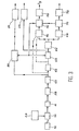
- FIG. 2 represents an embodiment of a device according to the invention.
- a semiconductor detector 14 of high resistivity (greater than 10 9 ⁇ .cm) is connected to a preamplifier 4, composed of an operational amplifier 6 and an integration capacitor 8.
- the capacitance is reaction and a resistor 10 which discharges the integrated load at its terminals.
- the detector is for example a detector based on cadmium telluride (CdTe or CdZnTe) or a detector based on HgI 2 or PbI 2 .
- the constituent materials of this detector are obtained for example by HPBM method: such a method allows to obtain materials whose resistivity is ten times greater than that of known materials usually used in ⁇ spectrometry (detectors operating at room temperature).
- a material is chosen for which the product of the mobility of the electrons by their lifetime is greater than 10 -4 cm 2 / volt.
- such a detector makes it possible to avoid the introduction of a decoupling capability between detector 14 and preamplifier 4.
- the detector has a thickness between 3 and 6 mm, and works with applied voltages between his two electrodes included between 100 and 500 volts.
- this detector can be operated at room temperature by a method and a device for correcting spectrometric measurements in the field of the detection of ⁇ photons, of the type of that described in EP-763 751
- the reference 16 designates a radiation source that emits ⁇ photons in direction of a detector 14, semiconductor, of the type described above.
- Means 54 are also provided which allow to choose the polarization of the detector.
- charge preamplifier 4 for example a preamplifier eV 5093.
- the output signal of the preamplifier 4 loads is transmitted to a playback preamplifier 58, whose gain can for example be adjusted between 1 and 3.
- Means may additionally be provided to adjust the polarity of the signal.
- the means 60 combine a amplifier and a high-pass filter. The high pass filter allows to reject any continuous component.
- the amplified and filtered signal then attacks a high-pass filter 62.
- This filter is used to reject the slow signal, that is the slow component of the signal which is due to the holes. In output, is thus obtained a signal that corresponds to the electronic component of the total signal.
- the time constant of the high-pass filter 62 is chosen very small in front of the time collection of holes and greater or equal or comparable to the time of collection of electrons.
- a signal representative of evolution time of the only electronic component is therefore transmitted to a peak detector 64 at the output of which is connected a discriminator 66 upward to the ridge of the signal.
- a transistor by example a transistor 2N 2894, charges a capacitor to the peak level of the signal. In output, a tension is observed, indicating that the transistor is charging the capacitor. As soon as the peak of the signal passes, the charging is stopped and the collector voltage is canceled.
- the signal obtained at the output of the discriminator 66 is transmitted to means 68 which make it possible to determine the end-of-rise time t 1 of the electronic component of the total signal.
- the collector voltage of the discriminator transistor 66 is applied to a comparator. Therefore, during charging, i.e. during the rise of the electronic component, a current of about 2 milliamperes is provided at the input of an integrator 70, whose integration capability is selected at the same time the constant of the high-pass filter 62.
- Logic signals control the integration phase.
- An amplifier-adapter 72 follows the integrator and provides a signal, or a voltage, proportional to the fast migration time which is a good approximation of the electron collection time, i.e., the rise time of the component electronic.
- the output signal of the discriminator 66 or the pre-amplified and filtered signal, taken out of means 60 or 62, is also used to trigger means 74 for detecting the threshold of the beginning of the rise of the signal. For this, the preamplified and filtered signal is compared at a low threshold. Crossing this low threshold causes the transmission of a signal at the output of means 74 to means 76 for triggering a sequence of integration in time and delivery to zero of the integrator 70 at the end of the sequence. Similarly, these means 76 transmit to the peak detector 64 a reset signal at the end of the sequence.
- a adapter 78 output means 76 can generate a synchronization signal Sy.
- the peak detector 80 takes a signal in output of the high pass filter amplifier assembly 60.
- This peak detector 80 may consist of similar to detector 64.
- an adapter 65, 81 allows to obtain a signal representative of the amplitude, that is, the load, the component electronic total signal, or the total signal itself (electronic component + hole component).
- the information relating to the rise time of the electronic component and the information relating to the amplitude, or the load, of the electronic component of the total signal, or of the total signal, same can be exploited by producing a representative signal, or representative data, of the maximum load Q m , or the maximum amplitude of the total signal, which should have been detected if the signal operated without losses.
- Correlation data can be previously established using a network of curves. Each measurement of a couple of data (rise time, amplitude or charge of the electronic component or total signal) can then be compared to such a network of curves.
- the principle is therefore to measure the rise time of the signal, its amplitude, and obtain the maximum amplitude which should have been measured thanks to the knowledge of the relationship, or correlation, between charges measured and the rise times.
- the signal comprises on the one hand an electronic component that corresponds to the collection of electrons, and on the other hand a hole component that corresponds to the collection of holes.
- the electronic component can be isolated or identified by temporal differentiation or filtering. We can thus find our in the case where only the electronic signal exists: we identify the amplitude of the measured signal Q m and the measured rise time ⁇ m , of the electronic component, and we compare these results with the correlations.
- the charge preamplifier is constituted (FIG. 1) of an amplifier A, with a capacitance feedback (or integration) 8 (Ci) and a counter-reaction resistance (Ri), intended to fix the rest point of the circuit.
- the impedance of the source determines the choice of the technology used.
- the current of the detector in the absence of signal, called of darkness, noted Ip, is not null and is generally variable with manufacture, temperature, etc.
- Resistance is of high value (typically greater than 50 megohm in the application presented), so that its current of noise is negligible in front of that of the detector.
- a binding capacity 12 (Cl) "cuts” this component and allows only the rapid variations in current, especially those produced by the useful signal due to the interaction of photon in the semiconductor material.
- the time constant Ti RixCi sets the frequency domain of integration (use) of the circuit. It is therefore related to the aspect time of the signal to be processed: in this case, the transit time of electrons, note te, in the semiconductor material: Ti >> te max (for example: Ti> 10 te max). te max is the maximum transit time electrons. For a given detector, it is determined once the voltage V applied to the terminals of it is fixed. It corresponds, in fact, in case the point of impact is located on the cathode or close to this one.
- RI x Ip ⁇ VDD the voltage power supply of the preamplifier (for example: Ri x Ip 1/2 VDD or 1/3 VDD or Ri Ip ⁇ VDD).
- Ri Ip depends then on the supply voltage VDD of the amplifier 6.
- a method of operation of a detection device the detector being placed under tension determined (so with a determined te max) and the amplifier being powered by a voltage VDD, will be such that: Ti >> te max, and / or Ri Ip ⁇ VDD.
- Figures 4A and 4B show the results obtained under the same conditions by injecting via a pulse generator a amplitude calibrated signal (high gain) and in time on a small capacity simulating the detector.
- This measurement allows you to calibrate in amplitude and in time the chain of acquisition and identify its possible non-linearity in order to deconvolute the influence of the detector and the chain on the quality of the measurement.
- times of 100 ns to 1 ⁇ s are measurable for amplitudes corresponding to 122 KeV.
- the noise associated with the measurement is weak for the amplifier alone (figure 4A) and much higher for the amplifier + the preamplifier (Figure 4B).
- Figure 5 shows the amplitude spectrum.
- this capacitance and the polarization resistance are suppressed.
- the chosen material very resistant (resistivity greater than 10 9 ⁇ .cm), operates under a low voltage (for example between 100 and 500 V), at room temperature.
- the advantage of imposing a low voltage of polarization is to increase the transit time of electrons, which makes it possible to measure rise times longer with a low noise. This remains possible as the electrons created under the cathode (and responsible for much of the pic 122 KeV) migrate throughout the thickness of the detector, ie both that the 122 KeV peak channel remains constant. A compromise is therefore to be found between the effectiveness of collection of electrons created under the cathode and the ability of electronics to measure the weak rise time of the electrons very close to the anode. This compromise depends on the thickness of the detectors and the polarization voltage applied.
- the other advantage of work at low bias voltage is to obtain a very weak current of darkness (10 nA to 100 nA) resulting in a slower aging of the detector and a reduction of the detector noise.
- Figure 6 shows that in a device according to the invention, the dark current is low enough not to saturate the preamplifier associated with the detector. The results were obtained with a system identical to that already described above, but without decoupling capability.
- the advantages of the device according to the invention are, among others, those already mentioned above (limitation of aging, risk of breakdown, and the noise of currents in the dark).
- a CdZnTe detector marketed by eV-Products, quality 5 mm thick spectrometer shows a detection efficiency of 26% ⁇ 5% and resolution in 5% energy at 122 KeV.
- the proposed correction method is based on the measurement of the electronic contribution to the signal, electrons having transport properties well greater than that of the holes. It is described in the EP-763 751.
- This method involves measuring the relationship between the amplitude and the rise time of the component of the electrons of the integrated signal. This relationship is quasi-linear and has the advantage of depend only on the mobility of electrons that varies very little along an ingot, and from one ingot to another. This improves the performance of the detectors which can be corrected, therefore usable, for a gamma camera.
- This method of correction is all the more effective that the thickness of the detector is higher and the lower bias voltage; this allows to increase the transit times of electrons and to improve the noise associated with their measurement.
- the suppression of detector-preamplifier binding capability loads improves performance of the correction method by a reduction of the noise measurement.
- a gamma camera can be realized. For example, it is possible to make a 20x20cm 2 cadmium telluride based camera derived from the HPBM growth method, and using the correction method described above. Approximately 1600 detectors can be juxtaposed, with dimensions close to 4x4x6 mm 3 .
- Such a gamma imaging device involves the realization of an integrated electronics using ASIC technology associated with a group of detectors (4 or 16 detectors). This electronics may comprise means for implementing the correction method described in document EP-763 751.
- the present invention (operation of high-resistivity detectors, without decoupling capability) makes it possible to improve the performance of the imaging device, in terms of resolution in energy, therefore of contrast of the image, and also makes it possible to reduce its costs of realization, because of the suppression of two electronic components (capacity of decoupling and resistance of polarization).
Description
L'invention relève du domaine de la détection de rayonnement γ, le détecteur utilisé étant un semi-conducteur. Elle concerne en outre le domaine des mesures spectrométriques en imagerie γ.The invention relates to the field of detection of γ radiation, the detector used being a semiconductor. It also concerns the field of spectrometric measurements in γ imaging.
De nombreux types de détecteurs ont été imaginés pour la détection de rayonnement γ. L'emploi de détecteur solide à base de semi-conducteurs a été le principal apport de ces 30 dernières années aux techniques de détection du rayonnement γ.Many types of detectors have been designed for the detection of γ radiation. employment Solid state detector based on semiconductors was the main contribution of the last 30 years to γ radiation detection techniques.
Les détecteurs à base de semi-conducteurs réalisent directement la conversion en énergie du rayonnement γ dans la matière, sans passer par des étapes intermédiaires, comme l'émission de photons visibles dans le cas des scintillateurs. On s'affranchit ainsi des problèmes de couplage synonymes de perte de rendement. L'énergie nécessaire pour créer une paire électron-trou dans un semi-conducteur est beaucoup plus faible que dans un gaz ou dans un scintillateur (environ 4eV dans les semi-conducteurs, contre 30eV dans les gaz, et 300eV dans les systèmes scintillateur photomultiplicateur). En conséquence, le nombre de charges libres créées par photon détecté est plus important, ce qui permet d'obtenir de meilleures résolutions en énergie, avec un faible bruit. De plus, le numéro atomique et la densité élevés des matériaux semi-conducteurs permettent d'utiliser des volumes de détection nettement inférieurs à ceux des détecteurs à gaz ou des scintillateurs, tout en conservant la même efficacité quantique de détection.Semiconductor-based detectors directly realize the energy conversion of the γ radiation in matter without going through intermediate steps, like photon emission visible in the case of scintillators. We thus avoids synonymous coupling problems yield loss. The energy needed to create an electron-hole pair in a semiconductor is much lower than in a gas or in a scintillator (about 4eV in semiconductors, against 30eV in the gases, and 300eV in the systems photomultiplier scintillator). As a result, number of free charges created by photon detected is more importantly, which allows for better energy resolutions, with low noise. Moreover, the atomic number and the high density of materials semiconductors make it possible to use volumes of significantly lower than the detectors at gas or scintillators, while maintaining the same quantum efficiency of detection.
L'utilisation de ces matériaux semi-conducteurs comme détecteurs de rayonnement X ou γ implique le dépôt de deux contacts électriques à la surface du matériau, aux bornes desquels une tension de polarisation est appliquée. Les porteurs de charges, c'est-à-dire les paires électron-trou créées par l'interaction du photon γ avec le matériau, vont se séparer sous l'action du champ électrique, les électrons migrant vers l'électrode positive et les trous vers l'électrode négative. L'aptitude de ces porteurs de charge à migrer vers les électrodes sans se faire piéger par des défauts présents dans le matériau semi-conducteur conditionnera la résolution en énergie du spectre mesuré. Cette aptitude, appelée aussi propriété de transport des porteurs de charge, est mesurée par la mobilité et la durée de vie des électrons et des trous.The use of these semiconductor materials as X or gamma radiation detectors involves the deposit of two electrical contacts on the surface of material, across which a voltage of polarization is applied. The carriers of charges, that is, the electron-hole pairs created by the interaction of the γ photon with the material, will to separate under the action of the electric field, the electrons migrating to the positive electrode and the holes to the negative electrode. The aptitude of these charge carriers to migrate to the electrodes without trapped by defects present in the material semiconductor will condition the resolution into energy measured spectrum. This skill, also called transport property of the charge carriers, is measured by the mobility and lifespan of electrons and holes.
La mesure spectrométrique de photons incidents consiste à détecter le maximum de photons dans le volume du détecteur, ce qui nécessite une forte épaisseur pour une meilleure efficacité quantique de détection, et à mesurer avec précision l'énergie déposée par le photon, ce qui nécessite un excellent rendement de collection des trous et électrons migrant respectivement vers l'électrode négative et positive. Ces deux paramètres (efficacité quantique de détection et efficacité de collection des porteurs de charge) sont antinomiques puisque le premier est proportionnel et le second inversement proportionnel à l'épaisseur du détecteur. The spectrometric measurement of incident photons to detect the maximum of photons in the detector volume, which requires a strong thickness for better quantum efficiency of detection, and accurately measure energy deposited by the photon, which requires an excellent collection yield of holes and electrons migrating respectively to the negative and positive electrode. These two parameters (quantum detection efficiency and collection efficiency of charge carriers) are antithetical since the former is proportional and the second inversely proportional to the thickness of the detector.
L'efficacité quantique de détection peut être améliorée en optimisant l'épaisseur du détecteur, par rapport au domaine d'application, car elle ne dépend que de la densité et du numéro atomique du détecteur (pour une énergie donnée des photons incidents).The quantum efficiency of detection can be improved by optimizing the thickness of the detector, by to the field of application because it does not depend on only the density and the atomic number of the detector (for a given energy of the incident photons).
Par contre, les performances des détecteurs γ actuels sont limités par la présence de défauts natifs dans les semi-conducteurs qui, en piégeant les porteurs de charge durant leur migration vers les électrodes, diminuent leur durée de vie et ainsi détériorent la résolution en énergie du détecteur. Ces défauts natifs apparaissent systématiquement durant la cristallogénèse du matériau semi-conducteur. La bibliographie portant sur l'étude de ces défauts est abondante et elle montre que la cristallogénèse de tous les semi-conducteurs de haute résistivité pouvant fonctionner à température ambiante n'est pas maítrisée au point de supprimer ces défauts.On the other hand, the performances of the γ detectors are limited by the presence of native defects in semiconductors who, by trapping the carriers charge during their migration to the electrodes, decrease their life and thus deteriorate the energy resolution of the detector. These native defects systematically appear during crystallogenesis semiconductor material. The bibliography on the study of these defects is abundant and it shows that the crystallogenesis of all the semiconductors of high resistivity that can operate at temperature ambient is not controlled to the point of removing these defaults.
L'efficacité de collection des porteurs de charge (trous et électrons) peut être améliorée selon différentes méthodes, présentées dans le document EP-763 751.The collection efficiency of the carriers of charge (holes and electrons) can be improved according to different methods, presented in the document EP-763 751.
Ce document présente également un procédé pour la correction de la mesure spectrométrique dans le domaine de la détection de photons γ.This document also presents a method for the correction of the spectrometric measurement in the field of detection of γ photons.
Ce procédé consiste à mesurer, non pas l'amplitude totale du signal total intégré (électron + trou) en fonction de son temps de montée (méthode dite de correction "trou", décrite dans FR-2 738 693), mais à mesurer l'amplitude de la contribution électronique seule en fonction de son seul temps de montée (méthode dite de correction "électron"). La mesure, et par conséquent la connaissance mathématique, de la fonction corrélant l'amplitude du signal électron et son temps de montée, permet de corriger l'amplitude mesurée associée à l'interaction de chaque photon dans tout le volume du détecteur.This process consists of measuring, not the total amplitude of the integrated total signal (electron + hole) according to its rise time (so-called correction device "hole", described in FR-2 738 693), but to measure the amplitude of the electronic contribution only according to its only rise time (method so-called "electron" correction). The measure, and by therefore the mathematical knowledge of the function correlating the amplitude of the electron signal and its time climb, corrects the measured amplitude associated with the interaction of each photon throughout the detector volume.
L'avantage de la correction "électron" est que la relation existant entre l'amplitude du signal électron et son temps de montée ne dépend que de la mobilité des électrons qui varie peu sur tout un lingot et d'un lingot à l'autre : la mobilité dépend principalement du réseau cristallin. Par contre, la correction "trous" dépend de la durée de vie des trous dont les variations sur un même lingot peuvent être importantes. En effet, cette durée de vie est imposée par les différents défauts créés lors de la cristallogénèse, qui est mal maítrisée. Une conséquence de ces différences est que la correction "électron" peut corriger les mesures dans la plupart des matériaux semi-conducteurs, ce qui n'est pas le cas de la correction "trou".The advantage of the "electron" correction is that the relationship between the amplitude of the signal electron and its rise time only depends on the electron mobility that varies little over an entire ingot and from one slug to another: mobility depends mainly of the crystalline lattice. On the other hand, correction "holes" depends on the life of the holes whose variations on the same ingot can be important. Indeed, this life is imposed by the different defects created during the crystallogenesis, which is poorly controlled. A consequence of these differences is that the correction "electron" can correct measurements in most materials semi-conductors, which is not the case for correction "hole".
Les deux documents cités ci-dessus exposent l'un et l'autre un dispositif pour réaliser ou pour corriger des mesures spectrométriques.The two documents cited above set out both a device for carrying out or for correct spectrometric measurements.
Dans les deux cas, on utilise un préamplificateur classique juste en sortie du détecteur, puis une électronique spécifique pour mesurer l'amplitude du signal (composante électronique dans EP-763 751 et signal global dans FR-2 738 693) et son temps de montée.In both cases, we use a classic preamplifier just out of the detector and then a specific electronics for measure the amplitude of the signal (electronic component in EP-763,751 and overall signal in FR-2,738,693) and its rise time.
Dans les deux cas, le signal est mesuré à l'aide d'un préamplificateur de charge classique acheté dans le commerce et connu de l'homme de l'art (exemple : préamplificateur 5093 acheté chez eV-Products). In both cases, the signal is measured at using a classic charging preamplifier bought in commerce and known to those skilled in the art (example: preamplifier 5093 purchased from eV-Products).
La figure 1 représente schématiquement un
détecteur 2, par exemple CdTe, et son préamplificateur
4.Figure 1 schematically represents a
La charge, déposée par le photon absorbé par le
détecteur 2, est intégrée aux bornes d'une capacité Ci
8 dite "d'intégration". Cette capacité est en contre
réaction avec une résistance Ri 10 (par l'utilisation
d'un préamplificateur opérationnel) qui permet de
"décharger" la charge intégrée aux bornes de la
capacité. C'est en fonction de la nature du semi-conducteur
et de la charge à mesurer que la constante
de temps Ri, Ci peut être adaptée.The charge, deposited by the photon absorbed by the
Dans tous les cas, le courant d'obscurité
associé au détecteur n'est pas mesuré et donc intégré
aux bornes de la capacité Ci, sa valeur absolue étant
encore beaucoup trop élevée. En effet, elle est
supérieure à la charge déposée par le photon
interagissant dans le détecteur. Elle dépend de la
résistivité du semi-conducteur mais aussi de la tension
de polarisation appliquée aux bornes du détecteur. Or,
la tension de polarisation doit être suffisante pour
collecter les charges déposées par chaque photon et
ainsi mesurer leur énergie. Les faibles propriétés de
transport des charges (mobilité et durée de vie)
nécessitent des tensions de polarisation (entre 100 et
500 volts selon l'épaisseur du détecteur) pour
lesquelles le courant d'obscurité reste élevé. Par
conséquent, une capacité 12 dite de "découplage" est
insérée entre le détecteur et la capacité. Cette
capacité 12 supprime la composante continue du courant
d'obscurité et seuls les impulsions transitoires
correspondant aux différentes interactions des photons
dans le détecteur, sont prises en compte. Ce principe
de mesure est aujourd'hui la seule configuration
possible du point de vue "électronique" autorisant la
mesure de la charge déposée sans que celle-ci soit
"noyée" par le courant d'obscurité.In all cases, the dark current associated with the detector is not measured and therefore integrated across the capacitance C i , its absolute value is still much too high. Indeed, it is greater than the charge deposited by the photon interacting in the detector. It depends on the resistivity of the semiconductor but also on the bias voltage applied across the detector. However, the bias voltage must be sufficient to collect the charges deposited by each photon and thus measure their energy. The low charge transport properties (mobility and lifetime) require bias voltages (between 100 and 500 volts depending on the thickness of the detector) for which the dark current remains high. Therefore, a so-called "decoupling"
Malheureusement, cette configuration n'est pas
optimale du point de vue électronique, en termes de
rapport signal/bruit, car l'introduction de la capacité
de "découplage" 12 a l'inconvénient de ramener une
« capacité parasite » entre l'entrée du
préamplificateur et la masse électrique (référence des
tensions). L'effet en sortie du préamplificateur en est
une multiplication de la tension de bruit du
préamplificateur dans le rapport Σ Cin / Ci, somme des
capacités par rapport à la masse sur Ci, capacité
d'intégration, d'où une augmentation de la composante
de bruit produit par le dispositif électronique
d'amplification.Unfortunately, this configuration is not optimal from the electronic point of view, in terms of signal-to-noise ratio, since the introduction of the "decoupling"
La suppression de la capacité de découplage a été réalisée dans une chaíne de spectrométrie classique (A.C. Huber et al. « High Performance, thermoelectrically cooled X-Ray and Gamma Ray detectors », Invited Paper at the International Conference on the Application of Accelerators in Research and Industry, Denton, Texas, USA, November 1994).The removal of decoupling capacity has was performed in a conventional spectrometry chain (A.C. Huber et al., High Performance, thermoelectrically cooled X-Ray and Gamma Ray detectors ", Invited Paper at the International Conference on the Application of Accelerators in Research and Industry, Denton, Texas, USA, November 1994).
Mais, il est alors nécessaire de refroidir le détecteur CdTe utilisé (à -30°C) afin de diminuer la valeur moyenne du courant d'obscurité. Les performances sont alors bonnes mais il est nécessaire d'utiliser des éléments Peltier pour chaque détecteur. Il en résulte une utilisation difficile, par exemple dans un système d'imagerie constitué de 1600 détecteurs.But, it is then necessary to cool the CdTe detector used (at -30 ° C) to reduce the average value of the dark current. Performances are then good but it is necessary to use Peltier elements for each detector. It results difficult use, for example in a system imaging consisting of 1600 detectors.
Des améliorations aux circuits de traitement des
signaux issus du préamplificateur sont décrites dans la
demande EP 0 763 751 A1 déjà cité et dans le brevet
US-A-3 792 255. Dans ce dernier, un circuit de mise en
forme comporte une ligne à retard placé en amont. Un
discriminateur et un circuit monostable ne permettent
le déclenchement du circuit de mise en forme qu'après
que le signal d'entrée ait atteint son niveau maximum.Improvements to the processing circuits of
signals from the preamplifier are described in
La demande de brevet EP 0 642 038 A2, décrit
l'emploi et l'amélioration d'un cristal CZT de
détection ayant une résistivité voisine de 1011 Ω.cm
pour la détection de rayonnements dans des puits de
forage, donc à température élevée.The
L'invention cherche à résoudre ce problème.The invention seeks to solve this problem.
Plus particulièrement, l'invention a pour objet un dispositif de détection de rayonnements gamma à base de semi-conducteur, comportant :
- un détecteur à semi-conducteurs, de résistivité supérieure à 109Ω.cm,
- un préamplificateur de charge situé directement en sortie du détecteur, sans capacité de découplage ni résistance de polarisation entre le détecteur et le préamplificateur.
- un dispositif pour l'exploitation d'un signal ou d'un ensemble de données représentatives de l'évolution temporelle d'un signal, fourni par ledit détecteur à semi-conducteur en réponse à l'interaction d'un photon γ avec le matériau semi-conducteur, ce dispositif comportant des moyens pour produire une donnée représentative, ou un signal représentatif, du temps de montée de la composante électronique du signal total fourni par le détecteur, c'est-à-dire de la composante du signal qui correspond à la collection des électrons provenant de l'interaction de chaque photon γ avec le matériau semi-conducteur,
- des moyens pour produire une donnée représentative, ou un signal représentatif, d'une amplitude de la composante électronique du signal ou bien d'une amplitude du signal total.
- a semiconductor detector with a resistivity greater than 10 9 Ω.cm,
- a charge preamplifier located directly at the output of the detector, without decoupling capability or polarization resistance between the detector and the preamplifier.
- a device for operating a signal or a set of data representative of the temporal evolution of a signal, provided by said semiconductor detector in response to the interaction of a γ photon with the material semiconductor device, this device comprising means for producing a representative datum, or a representative signal, of the rise time of the electronic component of the total signal supplied by the detector, that is to say of the component of the signal which corresponds to to the collection of electrons resulting from the interaction of each photon γ with the semiconductor material,
- means for producing a representative datum, or a representative signal, of an amplitude of the electronic component of the signal or of an amplitude of the total signal.
Avantageusement, le préamplificateur de charge est rapide et à bas bruit.Advantageously, the charge preamplifier is fast and low noise.
Un détecteur à semi-conducteur pour l'invention
peut être en tellure de cadmium (CdTe ou CdTe:Cl) ou en
CdZnTe (par exemple : CdZnTe:Cl) ou en HgI2 ou en PbI2
ou en GaAl ou en PbIn ; ce matériau est tiré par la
méthode dite "méthode Brigman haute pression" ("High
Pressure Bridgman Method" ou HPBM), et la résistivité
obtenue est dix fois supérieure à celle des matériaux
CdTe connus jusqu'alors (obtenus par "Traveling Heater
Method" ou THM, ou par "Bridgman Method" ou BM), à la
température ambiante. Le faible courant de polarisation
du détecteur peut alors être écoulé par la résistance
de contre-réaction, par la suppression de la capacité
de liaison 12 et de la résistance de polarisation 16.
On bénéficie ainsi de la disparition de la capacité
parasite de la capacité de liaison et donc d'une
amélioration du bruit propre de l'électronique associée
au détecteur.A semiconductor detector for the invention can be cadmium telluride (CdTe or CdTe: Cl) or CdZnTe (for example: CdZnTe: Cl) or HgI 2 or PbI 2 or GaAl or PbIn; this material is drawn by the method known as the "High Pressure Bridgman Method" (HPBM), and the resistivity obtained is ten times greater than that of the CdTe materials known until now (obtained by "Traveling Heater Method" or THM, or by "Bridgman Method" or BM), at room temperature. The low polarization current of the detector can then be exhausted by the negative feedback resistance, by the suppression of the
L'invention présente d'autres avantages dans le domaine de la détection de photons gamma. En particulier, la suppression de la capacité de découplage et de la résistance de polarisation associée permettent de réduire le nombre de composants associés à chaque détecteur, ce qui, dans le cas d'une structure matricielle, facilite la réalisation de l'électronique intégrée (dans le cas d'une réalisation de type ASIC), et limite son coût. Par ailleurs, il est possible d'utiliser une faible tension de polarisation aux bornes du détecteur, tout en maintenant d'excellentes performances de détection : ceci permet de limiter le courant d'obscurité, donc le vieillissement du détecteur, ainsi que le bruit associé à la mesure de la charge intégrée.The invention has other advantages in the field of gamma photon detection. In particular, the removal of the capacity to decoupling and associated polarization resistance reduce the number of associated components to each detector, which, in the case of a structure matrix, facilitates the realization of electronics integrated (in the case of an ASIC realization), and limits its cost. Moreover, it is possible to use a low bias voltage at detector terminals, while maintaining excellent detection performance: this limits the dark current, so the aging of the detector, as well as the noise associated with the measurement of integrated load.
L'utilisation de la méthode de correction du procédé d'exploitation tel que décrit dans le document EP-763 751 (méthode de correction "électron") permet d'améliorer très nettement, à température ambiante, les performances d'un détecteur à base de semi-conducteur, en termes de résolution en énergie et d'efficacité de détection. La combinaison de cette méthode avec l'utilisation d'un détecteur de résistivité supérieure à 109 Ω.cm, conformément à l'invention, permet de maintenir ces excellentes performances de détecteurs, tout en utilisant une très faible tension de polarisation aux bornes des électrodes déposées de part et d'autre des faces du détecteur. La très forte résistivité du détecteur utilisé, et l'utilisation de la méthode de correction électron » permettant d'améliorer les performances associées à la méthode de correction "électron", en supprimant la capacité de découplage à température ambiante.The use of the method of correction of the operating method as described in document EP-763 751 ("electron" correction method) makes it possible to improve very clearly, at ambient temperature, the performance of a detector based on semiconductor, in terms of energy resolution and detection efficiency. The combination of this method with the use of a resistivity detector greater than 10 9 Ω.cm, in accordance with the invention, makes it possible to maintain these excellent detector performance, while using a very low polarization voltage across the terminals. electrodes deposited on either side of the detector faces. The very high resistivity of the detector used, and the use of the method of electron correction "to improve the performance associated with the method of correction" electron ", removing the decoupling capacity at room temperature.
L'association du détecteur à forte résistivité, à la méthode de correction "électron" permet de réduire considérablement le courant d'obscurité, en valeur moyenne, ainsi que le bruit associé. L'obtention d'un très faible courant d'obscurité permet de supprimer la capacité de découplage et ainsi d'améliorer le bruit associé à la mesure.The combination of high resistivity detector, to the method of correction "electron" can reduce considerably the dark current, worth average, as well as the associated noise. Obtaining a very low dark current can suppress the decoupling capability and thus improve the noise associated with the measurement.
L'invention concerne également une gamma-caméra comportant un nombre N de détecteurs fonctionnant à température ambiante, de petite dimension, chaque détecteur étant du type décrit ci-dessus. On obtient donc un dispositif d'imagerie gamma à performances améliorées, notamment en terme de résolution en énergie et de contraste d'image. Par ailleurs, les coûts de réalisation sont réduits, par suppression de deux composants électroniques, la capacité de découplage et la résistance de polarisation de chaque détecteur.The invention also relates to a gamma camera having a number N of detectors operating at room temperature, small, each detector being of the type described above. We obtain so a performance gamma imaging device improved, especially in terms of energy resolution and image contrast. Moreover, the costs of realization are reduced, by deleting two electronic components, decoupling capability and the polarization resistance of each detector.
L'invention a également pour objet un procédé de détection de rayonnement gamma mettant en oeuvre le dispositif exposé ci-dessus.The subject of the invention is also a method of gamma radiation detection using the device set out above.
De toute façon, les caractéristiques et avantages de l'invention apparaítront mieux à la lumière de la description qui va suivre. Cette description porte sur les exemples de réalisation, donnés à titre explicatif et non limitatif, en se référant à des dessins annexés sur lesquels :
- La figure 1 représente un dispositif selon l'art antérieur.
- La figure 2 représente schématiquement un dispositif selon l'invention.
- La figure 3 représente un dispositif pour la correction de mesures spectrométriques dans le domaine de la détection de photons γ.
- La figure 4A et 4B représentent des résultats de calibrage d'une chaíne de mesure biparamétrique.
- La figure 5 représente un spectre en amplitude d'un dispositif de l'art antérieur, avec capacité de découplage.
- La figure 6 représente un spectre en amplitude d'un dispositif selon l'invention, sans capacité de découplage.
- FIG. 1 represents a device according to the prior art.
- Figure 2 schematically shows a device according to the invention.
- FIG. 3 represents a device for the correction of spectrometric measurements in the field of the detection of γ photons.
- FIGS. 4A and 4B show calibration results of a two-parameter measurement chain.
- FIG. 5 represents an amplitude spectrum of a device of the prior art, with decoupling capability.
- FIG. 6 represents an amplitude spectrum of a device according to the invention, without decoupling capability.
La figure 2 représente une réalisation d'un dispositif conforme à l'invention.FIG. 2 represents an embodiment of a device according to the invention.
Un détecteur à semi-conducteur 14, de haute
résistivité (supérieure à 109Ω.cm) est relié à un
préamplificateur 4, composé d'un amplificateur
opérationnel 6 et d'une capacité d'intégration 8. La
capacité est en contre-réaction ainsi qu'une résistance
10 qui permet de décharger la charge intégrée à ses
bornes. Le détecteur est par exemple un détecteur à
base de tellure de cadmium (CdTe ou CdZnTe) ou un
détecteur à base de HgI2 ou de PbI2. Les matériaux
constitutifs de ce détecteur sont obtenus par exemple
par méthode HPBM : une telle méthode permet d'obtenir
des matériaux dont la résistivité est dix fois
supérieure à celle des matériaux connus habituellement
utilisés en spectrométrie γ (détecteurs fonctionnant à
température ambiante).A
Selon un autre critère, on choisit un matériau pour lequel le produit de la mobilité des électrons par leur durée de vie est supérieur à 10-4 cm2/volt.According to another criterion, a material is chosen for which the product of the mobility of the electrons by their lifetime is greater than 10 -4 cm 2 / volt.
Selon l'invention, un tel détecteur permet
d'éviter l'introduction d'une capacité de découplage
entre le détecteur 14 et préamplificateur 4.According to the invention, such a detector makes it possible
to avoid the introduction of a decoupling capability
between
De préférence, le détecteur a une épaisseur comprise entre 3 et 6 mm, et fonctionne avec des tensions appliquées entre ses deux électrodes comprises entre 100 et 500 volts.Preferably, the detector has a thickness between 3 and 6 mm, and works with applied voltages between his two electrodes included between 100 and 500 volts.
De manière avantageuse, ce détecteur peut être exploité à température ambiante par un procédé et un dispositif de correction de mesures spectrométriques dans le domaine de la détection de photons γ, du type de celui décrit dans le document EP-763 751Advantageously, this detector can be operated at room temperature by a method and a device for correcting spectrometric measurements in the field of the detection of γ photons, of the type of that described in EP-763 751
Un tel dispositif va être brièvement rappelé en liaison avec la figure 3.Such a device will be briefly recalled in connection with Figure 3.
Sur cette figure, la référence 16 désigne une
source de rayonnement qui émet des photons γ en
direction d'un détecteur 14, à semi-conducteur, du type
décrit ci-dessus.In this figure, the
Des moyens 54 sont par ailleurs prévus qui permettent de choisir la polarisation du détecteur.Means 54 are also provided which allow to choose the polarization of the detector.
En réponse à l'interaction d'un photon γ avec
le matériau semi-conducteur du détecteur 14, des
charges sont collectées. Le signal correspondant aux
charges collectées est disponible en sortie du
préamplificateur de charges 4 (par exemple un
préamplificateur eV 5093).In response to the interaction of a γ photon with
the semiconductor material of the
Le signal de sortie du préamplificateur de
charges 4 est transmis à un préamplificateur de lecture
58, dont le gain peut par exemple être réglé entre 1 et
3. Des moyens peuvent en outre être prévus pour ajustez
la polarité du signal. Les moyens 60 combinent un
amplificateur et un filtre passe-haut. Le filtre passe-haut
permet de rejeter toute composante continue.The output signal of the preamplifier
4 loads is transmitted to a
Le signal amplifié et filtré attaque ensuite un
filtre passe-haut 62. Ce filtre permet de rejeter le
signal lent, c'est-à-dire la composante lente du signal
qui est due aux trous. En sortie, est donc obtenu un
signal qui correspond à la composante électronique du
signal total.The amplified and filtered signal then attacks a
high-
La constante de temps du filtre passe-haut 62
est choisie très petite devant le temps collection des
trous et supérieure ou égale ou comparable au temps de
collection des électrons.The time constant of the high-
Un signal représentatif de l'évolution
temporelle de la seule composante électronique est donc
transmis à un détecteur de crête 64 à la sortie duquel
est relié un discriminateur 66 de montée vers la crête
du signal. Pour ce dernier élément, un transistor, par
exemple un transistor 2N 2894, charge un condensateur
jusqu'au niveau crête du signal. En sortie, une tension
est observée, indiquant que le transistor charge le
condensateur. Dès le passage de la crête du signal, la
charge est arrêtée et la tension collecteur s'annule.A signal representative of evolution
time of the only electronic component is therefore
transmitted to a
Le signal obtenu en sortie du discriminateur 66
est transmis à des moyens 68 qui permettent de
déterminer l'instant de fin de montée t1 de la
composante électronique du signal total. La tension
collecteur du transistor du discriminateur 66 est
appliquée à un comparateur. Par conséquent, pendant la
charge, c'est-à-dire pendant la montée de la composante
électronique, un courant d'environ 2 milliampères est
fourni en entrée d'un intégrateur 70, dont la capacité
d'intégration est sélectionnée en même temps que la
constante du filtre passe-haut 62. Des signaux logiques
contrôlent la phase d'intégration. Un amplificateur-adaptateur
72 suit l'intégrateur et fournit un signal,
ou une tension, proportionnel au temps de migration
rapide qui est une bonne approximation du temps de
collection des électrons, c'est-à-dire du temps de
montée de la composante électronique.The signal obtained at the output of the
Le signal de sortie du discriminateur 66 ou le
signal préamplifié et filtré, prélevé en sortie des
moyens 60 ou 62, sert également à déclencher des moyens
74 de détection du seuil du début de montée du signal.
Pour cela, le signal préamplifié et filtré est comparé
à un seuil bas. Le franchissement de ce seuil bas
provoque la transmission d'un signal en sortie des
moyens 74 vers des moyens 76 de déclenchement d'une
séquence d'intégration dans le temps et de remise à
zéro de l'intégrateur 70 en fin de séquence. De même,
ces moyens 76 transmettent au détecteur crête 64 un
signal de remise à zéro en fin de séquence. Un
adaptateur 78 en sortie des moyens 76 permet de générer
un signal Sy de synchronisation.The output signal of the
Le détecteur crête 80 prélève un signal en
sortie de l'ensemble amplificateur-filtre passe-haut
60. Ce détecteur de crête 80 peut être constitué de
manière similaire au détecteur 64. En sortie de chacun
de ces détecteurs 64, 80 un adaptateur 65, 81 permet
d'obtenir un signal représentatif de l'amplitude,
c'est-à-dire de la charge, de la composante
électronique du signal total, ou du signal total lui-même
(composante électronique + composante trou). The
Comme expliqué dans le document EP-763 751, l'information portant sur le temps de montée de la composante électronique et l'information portant sur l'amplitude, ou la charge, de la composante électronique du signal total, ou du signal total lui-même, peut être exploitée en produisant un signal représentatif, ou une donnée représentative, de la charge maximale Qm, ou de l'amplitude maximale du signal total, qui aurait du être détecté si le signal fonctionnait sans pertes.As explained in the document EP-763 751, the information relating to the rise time of the electronic component and the information relating to the amplitude, or the load, of the electronic component of the total signal, or of the total signal, same, can be exploited by producing a representative signal, or representative data, of the maximum load Q m , or the maximum amplitude of the total signal, which should have been detected if the signal operated without losses.
Des données de corrélations peuvent être préalablement établies à l'aide d'un réseau de courbes. Chaque mesure d'un couple de données (temps de montée, amplitude ou charge de la composante électronique ou du signal total) peut alors être comparée à un tel réseau de courbes.Correlation data can be previously established using a network of curves. Each measurement of a couple of data (rise time, amplitude or charge of the electronic component or total signal) can then be compared to such a network of curves.
On peut également, au lieu d'un réseau de courbes, mémoriser toutes les données relatives aux corrélations (courbe, énergie) dans des moyens de mémorisation, par exemple dans un ordinateur conventionnel. L'attribution d'une mesure (Qm, τm) à une courbe et à une énergie donnée peut ensuite être réalisée par des moyens informatiques, par exemple à l'aide du même ordinateur spécialement programmé à cet effet. Des moyens d'affichage des données, sous forme graphique par exemple, peuvent également être prévus.It is also possible, instead of a network of curves, to store all the data relating to the correlations (curve, energy) in storage means, for example in a conventional computer. The assignment of a measurement (Q m , τ m ) to a curve and a given energy can then be performed by computer means, for example using the same computer specially programmed for this purpose. Data display means, in graphical form for example, may also be provided.
Il est ensuite possible d'effectuer une correction, soit par une électronique dédiée, soit par informatique. Quel que soit le cas de figure, le principe consiste donc à mesurer le temps de montée du signal, son amplitude, et obtenir l'amplitude maximale qui aurait due être mesurée grâce à la connaissance de la relation, ou de la corrélation, entre les charges mesurées et les temps de montée.It is then possible to perform a correction, either by dedicated electronics or by computer. Whatever the case, the principle is therefore to measure the rise time of the signal, its amplitude, and obtain the maximum amplitude which should have been measured thanks to the knowledge of the relationship, or correlation, between charges measured and the rise times.
Ainsi, si la corrélation établie est linéaire,
la charge Qc obtenue par correction est donnée par la
relation :
Tout ceci vaut aussi bien pour un matériau semi-conducteur ou seul le signal électronique subsiste, que pour un matériau semi-conducteur pour lequel le signal trou existe, si petit fut-il. Dans ce dernier cas, le signal comporte d'une part une composante électronique qui correspond à la collection des électrons, et d'autre part une composante trou qui correspond à la collection des trous. La composante électronique peut être isolée ou identifiée par différenciation temporelle ou filtrage. On peut ainsi se retrouver dans le cas où seul le signal électronique existe : on identifie l'amplitude du signal mesuré Qm et le temps de montée mesurée τm, de la composante électronique, et on compare ces résultats avec les corrélations.All this applies as well to a semiconductor material or only the electronic signal remains, as for a semiconductor material for which the signal hole exists, so small was it. In the latter case, the signal comprises on the one hand an electronic component that corresponds to the collection of electrons, and on the other hand a hole component that corresponds to the collection of holes. The electronic component can be isolated or identified by temporal differentiation or filtering. We can thus find ourselves in the case where only the electronic signal exists: we identify the amplitude of the measured signal Q m and the measured rise time τ m , of the electronic component, and we compare these results with the correlations.
On peut également, afin de disposer d'un rapport signal/bruit plus important, mesurer l'amplitude du signal total (composante électronique plus composante trou), le temps de montée de la composante électronique, et comparer ces données avec une corrélation préalablement établie entre l'amplitude totale de signaux et les temps de montée des composantes électroniques de ces signaux. Dans ce cas, les corrélations peuvent ne plus être linéaires mais, comme on l'a dit, le rapport signal/bruit est plus important. On obtient ainsi la charge totale maximale qui aurait due être mesurée si l'interaction s'était produite au voisinage de la cathode.One can also, in order to have a higher signal-to-noise ratio, measure the amplitude of the total signal (electronic component plus component hole), the rise time of the electronic component, and compare these data with a previously established correlation between amplitude total of signals and the rise times of electronic components of these signals. In that case, the correlations may no longer be linear but, as we said, the signal-to-noise ratio is more important. This gives the maximum total load which should have been measured if the interaction had produced near the cathode.
D'autres informations et exemples sur le procédé de traitement des données sont fournis dans le document EP-763 751.Other information and examples on the process of data processing are provided in the EP-763 751.
Un moyen classique d'exploiter le signal issu d'un détecteur solide type CdTe, activé par un photon, est le préamplificateur de charges 6 (figure 1).A classic way of exploiting the signal a solid detector type CdTe, activated by a photon, is the charge preamplifier 6 (Figure 1).
Le préamplificateur de charges est constitué (figure 1) d'un amplificateur A, d'une capacité de contre-réaction (ou d'intégration) 8 (Ci) et d'une résistance de contre-réaction 10 (Ri), destinée à fixer le point de repos du circuit.The charge preamplifier is constituted (FIG. 1) of an amplifier A, with a capacitance feedback (or integration) 8 (Ci) and a counter-reaction resistance (Ri), intended to fix the rest point of the circuit.
Fonctionnant en intégrateur, le préamplificateur de charges fournit une tension V proportionnelle à la charge Q reçue : V = Q/Ci.Operating as an integrator, the preamplifier loads provides a voltage V proportional to the received charge Q: V = Q / Ci.
L'amplificateur 6 présente, entre autres :
- un gain G (le plus grand possible)
- une tension et un courant de bruit (1 plus faible possible).
- a G gain (the largest possible)
- a voltage and a noise current (1 weakest possible).
Vis-à-vis du bruit, l'impédance de la source détermine le choix de la technologie utilisée.With respect to noise, the impedance of the source determines the choice of the technology used.
Un moyen classique de polariser le détecteur est de lui placer en série une résistance 3 (Rp) dans le circuit de polarisation, ici une source de haute-tension.A classic way to polarize the detector is to put him in series a resistance 3 (Rp) in the polarization circuit, here a source of high tension.
Le courant du détecteur, en l'absence de signal, dit d'obscurité, noté Ip, n'est pas nul et est généralement variable avec la fabrication, la température, etc.The current of the detector, in the absence of signal, called of darkness, noted Ip, is not null and is generally variable with manufacture, temperature, etc.
La résistance est de valeur élevée (typiquement supérieure à 50 megohm dans l'application présentée), pour que son courant de bruit soit négligeable devant celui du détecteur.Resistance is of high value (typically greater than 50 megohm in the application presented), so that its current of noise is negligible in front of that of the detector.
Il en résulte une différence de potentiel UO = Rpxlp aux bornes de la résistance, toute aussi variable.This results in a potential difference UO = Rpxlp across the resistance, just as variable.
Une capacité de liaison 12 (Cl), "coupe" cette composante continue et ne laisse passer que les variations rapides de courant, en particulier celles produites par le signal utile dû à l'interaction du photon dans le matériau semi-conducteur.A binding capacity 12 (Cl), "cuts" this component and allows only the rapid variations in current, especially those produced by the useful signal due to the interaction of photon in the semiconductor material.
On notera que tous les composants - résistance, capacité, amplificateur, etc. - ont une capacité par rapport à la masse commune d'alimentation constituant la référence des potentiels. Cette capacité, dite parasite, notée Cpar, a ici un effet multiplicateur, par Σ(Cpar)/Cf, de la tension de bruit Eea du préamplificateur.Note that all components - resistance, capacity, amplifier, etc. - have a capacity per relative to the common ground supply constituting the reference of potentials. This capacity, called parasite, noted Cpar, here has a multiplying effect, by Σ (Cpar) / Cf, the noise voltage Eea of preamplifier.
Pour des raisons d'augmentation des performances par diminution du bruit et/ou économiques (réduction des coûts) on peut souhaiter réduire le nombre de composants.For reasons of increasing performance by noise reduction and / or economic (cost reduction) we may wish to reduce the number of components.
On supprime la capacité de liaison Cl et on
confond ainsi la polarisation du détecteur avec la
contre-réaction du préamplificateur dans le même
composant, la résistance 10 Ri (figure 2).We suppress the Cl binding capacity and we
thus confuses the polarization of the detector with the
feedback from the preamplifier in the same
component, the
La constante de temps Ti = RixCi fixe le domaine fréquentiel d'intégration (d'utilisation) du circuit. Elle est donc en relation avec l'aspect temporel du signal à traiter : en l'occurrence, le temps de transit des électrons, note te, dans le matériau semi-conducteur : Ti >> te max (par exemple : Ti > 10 te max). te max est le temps de transit maximal des électrons. Pour un détecteur donné, il est déterminé une fois que la tension V appliquée aux bornes de celui-ci est fixée. Il correspond, en fait, au cas où le point d'impact est situé sur la cathode ou proche de celle-ci.The time constant Ti = RixCi sets the frequency domain of integration (use) of the circuit. It is therefore related to the aspect time of the signal to be processed: in this case, the transit time of electrons, note te, in the semiconductor material: Ti >> te max (for example: Ti> 10 te max). te max is the maximum transit time electrons. For a given detector, it is determined once the voltage V applied to the terminals of it is fixed. It corresponds, in fact, in case the point of impact is located on the cathode or close to this one.
De préférence, on cherche, par ailleurs, à ne
pas saturer l'amplificateur 6. La sortie et l'entrée du
préamplificateur sont donc de préférence comprises
entre 0 (la masse) et VDD. Pour cela, on cherche à
obtenir : RI x Ip < VDD, où VDD est la tension
d'alimentation du préamplificateur (par exemple :
Ri x Ip 1 / 2 VDD ou 1 / 3 VDD ou Ri Ip << VDD). Le produit
Ri Ip dépend donc alors de la tension d'alimentation
VDD de l'amplificateur 6.Preferably, one seeks, moreover, not to
not saturate the amplifier 6. The output and the input of
preamplifier are therefore preferably included
between 0 (mass) and VDD. For that, we try to
get: RI x Ip <VDD, where VDD is the voltage
power supply of the preamplifier (for example:
D'une manière générale, un procédé de fonctionnement d'un dispositif de détection selon l'invention, le détecteur étant placé sous une tension déterminée (donc avec un te max déterminé) et l'amplificateur étant alimenté par une tension VDD, sera tel que : Ti >> te max, et/ou Ri Ip < VDD.In general, a method of operation of a detection device according to the invention, the detector being placed under tension determined (so with a determined te max) and the amplifier being powered by a voltage VDD, will be such that: Ti >> te max, and / or Ri Ip <VDD.
Enfin, si on souhaite, de plus, l'obtention d'un rapport signal sur bruit grand ou maximum, on est conduit à choisir les valeurs de Ci la plus petite possible et de Ri la plus grande possible. Finally, if we wish, moreover, to obtain of a signal-to-noise ratio large or maximum, one is leads to choose the values of Ci the smallest possible and Ri the greatest possible.
Les caractéristiques du détecteur (te max, Ip) peuvent être telles que l'ensemble de ces contraintes a une solution réalisable :
- Ti=RixCi >> te max (≈ 1µs), compatible avec le domaine d'intégration lié au parcours des électrons,
- rapport signal/bruit grand => Ci < 0.5pF ; Ri > 50Mohm
- RixIp << VDD <=> Ip << VDD/Ri = 5/(5x107)=100nA, ce qui permet de ne pas saturer l'amplificateur (par exemple : Ip = 20nA ou Ip ≃ 20nA).
- Ti = RixCi >> te max (≈ 1μs), compatible with the integration domain related to the electron path,
- large signal-to-noise ratio => Ci <0.5pF;Ri> 50Mohm
- RixIp << VDD <=> Ip << VDD / Ri = 5 / (5x10 7 ) = 100nA, which makes it possible not to saturate the amplifier (for example: Ip = 20nA or Ip ≃ 20nA).
Ces conditions expriment la compatibilité avec le détecteur.These conditions express compatibility with the detector.
Compte tenu des valeurs très faibles de capacité rencontrées, on conçoit l'intérêt qu'apporte la miniaturisation des composants. L'obtention de telles valeurs, très difficile en électronique entièrement discrète, possible puisqu'existante en électronique hybride, est tout à fait réalisable en électronique intégrée.Given the very low values of capacity, we can see the interest that comes from the miniaturization of the components. Obtaining such values, very difficult in electronics completely discreet, possible since existing in hybrid electronics, is quite feasible in integrated electronics.
De tels circuits ont été réalisés en technologie CMOS 0,8µm.Such circuits have been realized in 0.8μm CMOS technology.
Des mesures comparatives ont été effectuées sur des spectres biparamétriques et des spectres d'amplitude, pour un dispositif de l'art antérieur (avec capacité de découplage) et un dispositif selon l'invention (en l'absence de capacité de découplage).Comparative measurements were made on biparametric spectra and spectra amplitude, for a device of the prior art (with decoupling capability) and a device the invention (in the absence of decoupling capability).
Pour le dispositif de l'art antérieur, les résultats ont été obtenus dans les conditions suivantes :
- source cobalt 57 DP343 (3,2 MBq le 17/11/93), avec 83% des photons émis à 122 KeV,
- collimateur tungstène ( 2,5 mm),
- détecteur CdZnTe 5x5x5 mm3 acheté à eV-Products n°eV-01100 qualité spectrométrique,
- tension de polarisation : 250 volts,
- connectique et distance détecteur-capacité de liaison optimisés,
- préamplificateur n°eV-5093 avec capacité de liaison,
- amplificateur 2ème tiroir,
- programme d'acquisition et de correction développés sur labview.
- cobalt 57 DP343 source (3.2 MBq on 17/11/93), with 83% of photons emitted at 122 KeV,
- tungsten collimator ( 2.5 mm),
- CdZnTe detector 5x5x5 mm 3 purchased from eV-Products no. eV-01100 spectrometric quality,
- bias voltage: 250 volts,
- Connectivity and distance detector-link capacity optimized,
- preamplifier no. eV-5093 with connection capacity,
- 2nd drawer amplifier,
- acquisition and correction program developed on labview.
Les figures 4A et 4B présentent les résultats obtenus dans les mêmes conditions en injectant via un générateur d'impulsion un signal calibré en amplitude (gain élevé) et en temps sur une petite capacité simulant le détecteur. Cette mesure permet de calibrer en amplitude et en temps la chaíne d'acquisition et d'identifier ses éventuelles non linéarité afin de déconvoluer l'influence du détecteur et de la chaíne électronique sur la qualité de la mesure. On observe que des temps de 100 ns à 1 µs sont mesurables pour des amplitudes correspondant à 122 KeV. Le bruit associé à la mesure est faible pour l'amplificateur seul (figure 4A) et beaucoup plus élevé pour l'amplificateur + le préamplificateur (figure 4B).Figures 4A and 4B show the results obtained under the same conditions by injecting via a pulse generator a amplitude calibrated signal (high gain) and in time on a small capacity simulating the detector. This measurement allows you to calibrate in amplitude and in time the chain of acquisition and identify its possible non-linearity in order to deconvolute the influence of the detector and the chain on the quality of the measurement. We observe that times of 100 ns to 1 μs are measurable for amplitudes corresponding to 122 KeV. The noise associated with the measurement is weak for the amplifier alone (figure 4A) and much higher for the amplifier + the preamplifier (Figure 4B).
Un spectre en amplitude de l'échantillon eV-01100, dans les conditions ci-dessus, est présentée sur la figure 5.An amplitude spectrum of the sample eV-01100, under the conditions above, is presented in Figure 5.
Sur le spectre biparamétrique amplitude-temps de montée (non représenté), on observe une relation amplitude-temps de montée peu bruitée sur une grande dynamique d'amplitude et de temps. Cette relation est mesurable sur le pic 122 KeV, et surtout sur le pic 136 KeV, ce qui témoigne de la finesse de la mesure et par conséquent de la qualité de l'électronique. La comparaison de la figure 4B et d'un tel spectre démontre que le bruit associé à la mesure de la relation amplitude-temps de montée est en grande partie dû au préamplificateur et non aux fluctuations du détecteur. Cette relation entre l'amplitude et le temps de montée permettra de corriger la mauvaise efficacité de collection des charges et ainsi d'améliorer les performances du détecteur. Les curseurs verticaux espacés de deux fois la largeur à mi-hauteur du pic permettent d'évaluer l'efficacité de détection du pic 122 KeV à environ 25% ±2%. Elle est calculée en effectuant le rapport (nombre de coups entre les deux curseurs)/(nombre de photons incidents calculé à l'aide de l'activité de la source, du collimateur et de la géométrie d'irradiation comprenant le collimateur). Le nombre de photons 122 KeV incidents est donné par le débit de photons incidents à sa surface (Inc. Counts=420 photons/seconde), le pourcentage de photons 122 KeV émis par la source cobalt 57 déduit de ceux qui créent l'échappement (85,7-3=83%) et le temps d'acquisition (900 secondes).On the amplitude-time biparametric spectrum of climb (not shown), a relationship is observed amplitude-rise time little noisy on a large dynamic amplitude and time. This relationship is measurable on the 122 KeV peak, and especially on the peak 136 KeV, which testifies to the delicacy of the measure and consequent quality of electronics. The comparison of Figure 4B and such a spectrum demonstrates that the noise associated with measuring the amplitude-rise time relationship is largely due to the preamplifier and not to the fluctuations of detector. This relationship between amplitude and time climb will correct the poor efficiency collects charges and thus improve the detector performance. Vertical sliders spaced twice the width halfway up the peak allow to evaluate the detection efficiency of the peak 122 KeV at about 25% ± 2%. It is calculated in performing the report (number of strokes between the two sliders) / (number of incident photons calculated using of the activity of the source, the collimator and the irradiation geometry including the collimator). The number of 122 KeV photons incident is given by the flow of photons incident on its surface (Inc. Counts = 420 photons / second), the percentage of photons 122 KeV emitted by cobalt source 57 inferred from those create the exhaust (85,7-3 = 83%) and the time acquisition (900 seconds).
La figure 5 représente le spectre en amplitude. La tension de polarisation a été fixée à 250 volts ce qui dégrade le pic sur vallée (P/V=2 contre P/V=3 à 850 volts) et la résolution en énergie (R=11% contre R=4,5% à 850 volts).Figure 5 shows the amplitude spectrum. The bias voltage was set at 250 volts this which degrades the peak on the valley (P / V = 2 against P / V = 3 to 850 volts) and the energy resolution (R = 11% against R = 4.5% at 850 volts).
Les mesures présentées ci-dessus ont été réalisées avec une capacité de liaison entre le détecteur et le préamplificateur. Cette capacité permet de s'affranchir de la valeur moyenne du courant d'obscurité. The measures presented above have been realized with a capacity of connection between the detector and the preamplifier. This ability allows to get rid of the average value of the current darkness.
Selon l'invention, cette capacité et la résistance de polarisation sont supprimées. Le matériau choisi, très résistant (résistivité supérieure à 109Ω.cm), fonctionne sous une faible tension (comprise par exemple entre 100 et 500 V), à température ambiante.According to the invention, this capacitance and the polarization resistance are suppressed. The chosen material, very resistant (resistivity greater than 10 9 Ω.cm), operates under a low voltage (for example between 100 and 500 V), at room temperature.
L'avantage d'imposer une faible tension de polarisation est d'augmenter le temps de transit des électrons, ce qui permet de mesurer des temps de montée plus longs avec un faible bruit. Cela reste possible tant que les électrons créés sous la cathode (et responsables en grande partie du pic 122 KeV) migrent sur toute l'épaisseur du détecteur, c'est-à-dire tant que le canal du pic 122 KeV reste constant. Un compromis est donc à trouver entre l'efficacité de collection des électrons créés sous la cathode et l'aptitude de l'électronique à mesurer les faibles temps de montée des électrons très près de l'anode. Ce compromis dépend de l'épaisseur des détecteurs et de la tension de polarisation appliquée. L'autre avantage de travailler à faible tension de polarisation est d'obtenir un très faible courant d'obscurité (10 nA à 100 nA) d'où un vieillissement moins rapide du détecteur et une diminution du bruit du détecteur.The advantage of imposing a low voltage of polarization is to increase the transit time of electrons, which makes it possible to measure rise times longer with a low noise. This remains possible as the electrons created under the cathode (and responsible for much of the pic 122 KeV) migrate throughout the thickness of the detector, ie both that the 122 KeV peak channel remains constant. A compromise is therefore to be found between the effectiveness of collection of electrons created under the cathode and the ability of electronics to measure the weak rise time of the electrons very close to the anode. This compromise depends on the thickness of the detectors and the polarization voltage applied. The other advantage of work at low bias voltage is to obtain a very weak current of darkness (10 nA to 100 nA) resulting in a slower aging of the detector and a reduction of the detector noise.
Outre le fait d'augmenter les temps de transit des électrons, ce qui facilite la mesure du temps de montée associé à de faibles amplitudes, l'utilisation d'une faible tension de polarisation (250 volts sur une épaisseur de 5 mm) présente d'autres avantages :
- le détecteur vieillit moins vite,
- les risques de claquages sont limités,
- le bruit associé au courant d'obscurité est plus faible et constant dans le temps.
- the detector ages less quickly,
- the risks of breakdowns are limited,
- the noise associated with the dark current is lower and constant over time.
La figure 6 montre que, dans un dispositif selon l'invention, le courant d'obscurité est suffisamment faible pour ne pas saturer le préamplificateur associé au détecteur. Les résultats ont été obtenus avec un système identique à celui déjà décrit ci-dessus, mais sans capacité de découplage.Figure 6 shows that in a device according to the invention, the dark current is low enough not to saturate the preamplifier associated with the detector. The results were obtained with a system identical to that already described above, but without decoupling capability.
Les résultats montrent une nette amélioration de la résolution en énergie : R=7% sans capacité (figure 6) contre R=11% avec capacité (figure 5). La suppression de cette capacité de liaison a permis d'améliorer le bruit associé au signal détecteur, ce qui améliore la finesse de la relation amplitude-temps de montée (figure 6, sans capacité, à comparer avec la figure 5, avec capacité).The results show a clear improvement the resolution in energy: R = 7% without capacity (Figure 6) against R = 11% with capacity (Figure 5). The removal of this binding ability allowed to improve the noise associated with the detector signal, this which improves the smoothness of the amplitude-time relationship climb (Figure 6, without capacity, to compare with the Figure 5, with capacity).
Les avantages du dispositif selon l'invention sont, entre autres, ceux déjà cités ci-dessus (limitation du vieillissement, des risques de claquage, et du bruit des courants à l'obscurité).The advantages of the device according to the invention are, among others, those already mentioned above (limitation of aging, risk of breakdown, and the noise of currents in the dark).
De plus, on constate de meilleures performances (réduction du bruit de mesure) pour un plus faible coût (l'implantation d'une capacité et d'une résistance est coûteuse).In addition, there is better performance (measurement noise reduction) for a lower cost (the implantation of a capacity and a resistance is expensive).
Avant toute correction, un détecteur CdZnTe, commercialisé par eV-Products, de qualité spectrométrique de 5 mm d'épaisseur présente une efficacité de détection de 26% ±5% et une résolution en énergie de 5% à 122 KeV.Before any correction, a CdZnTe detector, marketed by eV-Products, quality 5 mm thick spectrometer shows a detection efficiency of 26% ± 5% and resolution in 5% energy at 122 KeV.
La méthode de correction proposée est basée sur la mesure de la contribution électronique au signal, les électrons ayant des propriétés de transport bien supérieures à celle des trous. Elle est décrite dans le document EP-763 751. The proposed correction method is based on the measurement of the electronic contribution to the signal, electrons having transport properties well greater than that of the holes. It is described in the EP-763 751.
Cette méthode consiste à mesurer la relation entre l'amplitude et le temps de montée de la composante des électrons du signal intégré. Cette relation est quasi-linéaire et présente l'avantage de ne dépendre que de la mobilité des électrons qui varie très peu le long d'un lingot, et d'un lingot à l'autre. Cela permet d'améliorer le rendement des détecteurs pouvant être corrigés, donc utilisables, pour une gamma-caméra.This method involves measuring the relationship between the amplitude and the rise time of the component of the electrons of the integrated signal. This relationship is quasi-linear and has the advantage of depend only on the mobility of electrons that varies very little along an ingot, and from one ingot to another. This improves the performance of the detectors which can be corrected, therefore usable, for a gamma camera.
Cette méthode de correction est d'autant plus efficace que l'épaisseur du détecteur est plus élevée et la tension de polarisation plus faible ; cela permet d'augmenter les temps de transit des électrons et d'améliorer ainsi le bruit associé à leur mesure. La suppression de la capacité de liaison détecteur-préamplificateur de charges améliore les performances de la méthode de correction par une diminution du bruit de mesure.This method of correction is all the more effective that the thickness of the detector is higher and the lower bias voltage; this allows to increase the transit times of electrons and to improve the noise associated with their measurement. The suppression of detector-preamplifier binding capability loads improves performance of the correction method by a reduction of the noise measurement.
Selon un autre aspect de l'invention, une gamma-caméra peut être réalisée. Par exemple, on peut réaliser une caméra 20x20cm2, à base de tellure de cadmium, issu de la méthode de croissance HPBM, et utilisant la méthode de correction décrite ci-dessus. On peut juxtaposer environ 1600 détecteurs, avec des dimensions proches de 4x4x6 mm3. Un tel dispositif d'imagerie en rayonnement gamma implique la réalisation d'une électronique intégrée utilisant la technologie ASIC associée à un groupe de détecteurs (4 ou 16 détecteurs). Cette électronique peut comporter des moyens de réalisation de la méthode de correction décrite dans le document EP-763 751. La présente invention (fonctionnement de détecteurs à haute résistivité, sans capacité de découplage) permet d'améliorer les performances du dispositif d'imagerie, en terme de résolution en énergie, donc de contraste de l'image, et permet également de réduire ses coûts de réalisation, du fait de la suppression de deux composants électroniques (capacité de découplage et résistance de polarisation).According to another aspect of the invention, a gamma camera can be realized. For example, it is possible to make a 20x20cm 2 cadmium telluride based camera derived from the HPBM growth method, and using the correction method described above. Approximately 1600 detectors can be juxtaposed, with dimensions close to 4x4x6 mm 3 . Such a gamma imaging device involves the realization of an integrated electronics using ASIC technology associated with a group of detectors (4 or 16 detectors). This electronics may comprise means for implementing the correction method described in document EP-763 751. The present invention (operation of high-resistivity detectors, without decoupling capability) makes it possible to improve the performance of the imaging device, in terms of resolution in energy, therefore of contrast of the image, and also makes it possible to reduce its costs of realization, because of the suppression of two electronic components (capacity of decoupling and resistance of polarization).
Claims (21)
- Semiconductor based device for the detection of gamma radiation comprising:characterized in thata semiconductor based detector (14),an operational preamplifier (4) coupled to the detector,a device for the use of a signal or a plurality of signals or a set of data or a plurality of data sets representative of the variation with time of a signal supplied by the said semiconductor based detector (14) in response to the interaction of a γ photon with the semiconducting material, this device comprising means (58, 60, 62, 64, 66, 68, 70, 72) of producing data or a signal representative of the rise time of the electronic component of the total signal supplied by the detector, in other words the component of the signal that corresponds to the collection of electrons resulting from the interaction between each γ photon and the semiconducting material andmeans (65, 81) for producing a representative data unit or a representative signal of an amplitude of the electronic component of the signal or an amplitude of the total signal,the semiconductor of the detector has a resistivity above 109 Ω.cm,the preamplifier (4) is located directly at the output of the detector (14) without a decoupling capacitance between the detector (14) and the preamplifier (4).
- Device according to claim 1, characterized in that the device for exploiting a signal or a plurality of signals or a set of data or a plurality of data sets, each being representative of the time evolution of a signal supplied by the semiconductor based detector (14), also incorporates means (65, 81) for producing a representative data unit or a representative signal, either of the total detected charge, or of that part of the total charge resulting from the collection of electrons.
- Device according to claim 1, characterized in that the device for the exploitation of a signal or a plurality of signals or a set of data or a plurality of data sets, each being representative of the time evolution of a signal supplied by the semiconductor based detector (14), also has means for producing a representative signal, or a data unit representative of the maximum electrical charge or the maximum charge corresponding to at least part of a first data set representing the rise times of electronic components and a second data set representing the total detected charges or the charges resulting from the collection of electrons and means making it possible to establish a relation or correlation between the first and second data sets.
- Device according to claim 3, characterized in that the means for determining a maximum electric charge effect this on the basis of:signals or data concerning:the rise time of the signal electronic component,the total charge detected or that part of the total charge resulting from the collection of electrons,and on the basis of the relation or correlation between the first data set and the second data set.
- Device according to claim 4, also having means for correcting the measured charge on the basis of the maximum charge, the rise time corresponding to said maximum charge and the effectively measured rise time.
- Device according to any one of claims 1 to 5, the product of the mobility of electrons in the semiconductor by their life being greater than 10-4 cm2/V.
- Device according to either of the claims 1 or 6, the detector being made of CdTe or CdTe:Cl or CdZnTe:Cl or CdTeSe:Cl or CdZnTe or HgI2 or PbI2 or GaAs or PbIn.
- Device according to any one of claims 1 to 7, the material from which the semiconductor is made being obtained using the HPBM method.
- Device according to any one of claims 1 to 8, the thickness of the detector being between 3 mm and 6 mm.
- Process for the detection of gamma radiation, making use of a device according to either of the claims 1 and 2 at ambient temperature, and a step in which exploitation takes place of signal or a set of data representative of the variation with time of a signal supplied by the semiconductor based detector (14) in response to the interaction of a γ photon with the semiconducting material, data or a signal being produced in the semiconducting material representative of the rise time of the electronic component of the signal supplied by the detector, in other words the component of the total signal that corresponds to the collection of electrons resulting from the interaction between each γ photon and the semiconducting material.
- Process according to claim 10, which also produces data or a signal representative of either the total detected charge or the part of the total charge resulting from the collection of electrons.
- Process according to either of claims 10 and 11, which also produces data or a signal representative of either the amplitude of the signal output by the detector, or the amplitude of the electronic component of the signal supplied by the detector.
- Process for the detection of gamma radiation at ambient temperature according to claim 10, making use of a device according to claim 3, and also involving the establishment of a relation or correlation between on the one hand a first set of data representing the rise times of the electronic components and on the other a second data set representing either the total detected charges or those parts of the total charges resulting from the collection of electrons.
- Process according to claim 13, wherein determination takes place or production takes place of a data unit or a signal representative of the maximum electronic charge or the maximum charge corresponding to at least part of the first and second data sets.
- Process for the detection of gamma radiation according to claim 11 using, at ambient temperature, a device according to either of the claims 4 and 5, wherein:a maximum electrical charge is determined on the basis of:signals or data concerning:the rise time of the signal electronic component,and the total detected charge or that part of the total charge resulting from the collection of electrons,and on the basis of a relation or correlation between on the one hand a first data set representing the rise time of the electronic components and on the other a second data set representing either the total detected charges or those parts of the total charges resulting from the collection of electrons.
- Process according to claim 15, wherein correction takes place of the measured charge on the basis of the maximum charge, the rise time corresponding to said maximum charge and the effectively measured rise time.
- Process according to any one of claims 10 to 16, in which the voltage applied to the detector is between 100 and 500 V.
- Process according to claims 10 to 16, the detector (14) operating at a determined voltage V, therefore having a determined maximum electronic transit time to max, the preamplifier (14) being associated with a counter-reaction capacitor Ci (8) and a counter-reaction resistor Ri (10) where Ci and Ri are such that:
- Process according to claims 10 to 17, the detector having a darkness current Ip, the preamplifier (14) being associated with a counter-reaction capacitor Ci (8) and a counter-reaction resistor Ri (10), the preamplifier being powered at a voltage VDD, and Ri, Ip and VDD being such that:
- Use at ambient temperature of a device according to one of the claims 1 to 9, for the detection of gamma radiation, the detector (14) operating under a given voltage V, i.e. having a maximum electron transit time te max of a given nature, the preamplifier (14) being associated with a counter-reaction capacitor Ci (8) and a counter-reaction resistor Ri (10), Ci and Ri being such that:
- Use at ambient temperature of a device according to one of the claims 1 to 9, for the detection of gamma radiation, the detector having a darkness current Ip, the preamplifier (14) being associated with a counter-reaction capacitor Ci (8) and a counter-reaction resistor Ri (10), the preamplifier being powered under a voltage VDD, Ri, Ip and VDD being such that:
Applications Claiming Priority (3)
| Application Number | Priority Date | Filing Date | Title |
|---|---|---|---|
| FR9710392 | 1997-08-14 | ||
| FR9710392A FR2767387B1 (en) | 1997-08-14 | 1997-08-14 | DEVICE FOR SPECTROMETRIC MEASUREMENT IN THE FIELD OF GAMMA PHOTON DETECTION |
| PCT/FR1998/001807 WO1999009432A1 (en) | 1997-08-14 | 1998-08-14 | SPECTROMETRY MEASURING DEVICE IN THE FIELD OF PHOTON η DETECTION |
Publications (2)
| Publication Number | Publication Date |
|---|---|
| EP1004040A1 EP1004040A1 (en) | 2000-05-31 |
| EP1004040B1 true EP1004040B1 (en) | 2003-01-22 |
Family
ID=9510317
Family Applications (1)
| Application Number | Title | Priority Date | Filing Date |
|---|---|---|---|
| EP98942742A Expired - Lifetime EP1004040B1 (en) | 1997-08-14 | 1998-08-14 | Spectrometry measuring device in the field of photon gamma detection |
Country Status (6)
| Country | Link |
|---|---|
| US (1) | US6420710B1 (en) |
| EP (1) | EP1004040B1 (en) |
| JP (1) | JP2001516033A (en) |
| DE (1) | DE69810933T2 (en) |
| FR (1) | FR2767387B1 (en) |
| WO (1) | WO1999009432A1 (en) |
Cited By (1)
| Publication number | Priority date | Publication date | Assignee | Title |
|---|---|---|---|---|
| US9360568B2 (en) | 2009-10-07 | 2016-06-07 | Commissariat A L'energie Atomique Et Aux Energies Alternatives | Method for processing data derived from an ionizing radiation detector |
Families Citing this family (16)
| Publication number | Priority date | Publication date | Assignee | Title |
|---|---|---|---|---|
| JP2002350552A (en) * | 2001-05-28 | 2002-12-04 | Mitsubishi Electric Corp | Radiation detector |
| JP4269653B2 (en) * | 2002-11-20 | 2009-05-27 | 株式会社島津製作所 | Manufacturing method of radiation detector |
| FR2847676B1 (en) * | 2002-11-25 | 2005-02-11 | Commissariat Energie Atomique | IMPROVED TREATMENT CUIRCUIT FOR SPECTROMETRY CHAIN AND SPECTROMETRY CHAIN USING SUCH CIRCUIT |
| US7847260B2 (en) | 2005-02-04 | 2010-12-07 | Dan Inbar | Nuclear threat detection |
| US7820977B2 (en) | 2005-02-04 | 2010-10-26 | Steve Beer | Methods and apparatus for improved gamma spectra generation |
| US8173970B2 (en) | 2005-02-04 | 2012-05-08 | Dan Inbar | Detection of nuclear materials |
| JP2008533469A (en) * | 2005-03-10 | 2008-08-21 | トゥー‐シックス・インコーポレイテッド | Radiation detection system with improved signal discriminator and its use |
| JP5100986B2 (en) * | 2005-07-14 | 2012-12-19 | 株式会社神戸製鋼所 | Semiconductor carrier lifetime measuring device, semiconductor carrier lifetime measuring method |
| JP4670704B2 (en) * | 2006-03-31 | 2011-04-13 | 株式会社日立製作所 | Energy calibration method, energy region of interest setting method, radiation detection apparatus, and nuclear medicine diagnostic apparatus |
| US7576326B2 (en) * | 2006-06-07 | 2009-08-18 | Xrf Corporation | Devices and methods for detecting and analyzing radiation |
| FR2951036A1 (en) * | 2009-10-01 | 2011-04-08 | Commissariat Energie Atomique | DEVICE FOR PROCESSING A SIGNAL DELIVERED BY A RADIATION DETECTOR |
| JP5953116B2 (en) * | 2012-05-18 | 2016-07-20 | Jx金属株式会社 | Compound semiconductor crystal for radiation detection element, radiation detection element, and radiation detector |
| US9910168B2 (en) * | 2014-05-05 | 2018-03-06 | Raytheon Company | Combined neutron and gamma-ray detector and method |
| FR3058230B1 (en) * | 2016-10-27 | 2019-03-15 | Detection Technology Sas | SPECTROMETRY DEVICE |
| CN112449685B (en) * | 2018-07-12 | 2023-08-01 | 深圳帧观德芯科技有限公司 | Radiation detector |
| DE102019104710B4 (en) * | 2019-02-25 | 2023-04-27 | Ketek Gmbh | Method of operating a radiation detection system and radiation detection system |
Family Cites Families (7)
| Publication number | Priority date | Publication date | Assignee | Title |
|---|---|---|---|---|
| GB1359883A (en) * | 1971-02-05 | 1974-07-17 | Atomic Energy Authority Uk | Nuclear particle responsive arrangements |
| US4243885A (en) * | 1979-09-25 | 1981-01-06 | The United States Of America As Represented By The United States Department Of Energy | Cadmium telluride photovoltaic radiation detector |
| FR2693033B1 (en) * | 1992-06-30 | 1994-08-19 | Commissariat Energie Atomique | Large imaging device. |
| US5528495A (en) * | 1993-09-01 | 1996-06-18 | Schlumberger Technology Corporation | Cadmium zinc telluride borehole detector |
| US5627377A (en) * | 1995-09-07 | 1997-05-06 | Santa Barbara Research Center | Single carrier-type solid-state radiation detector device |
| FR2738693B1 (en) * | 1995-09-12 | 1997-10-10 | Commissariat Energie Atomique | PULSE PROCESSING SYSTEM ARISING FROM THE INTERACTION OF A GAMMA PARTICLE WITH A CDTE RADIATION DETECTOR |
| FR2738919B1 (en) * | 1995-09-15 | 1997-10-17 | Commissariat Energie Atomique | METHOD AND DEVICE FOR THE CORRECTION OF SPECTROMETRIC MEASUREMENT IN THE FIELD OF GAMMA PHOTON DETECTION |
-
1997
- 1997-08-14 US US09/463,973 patent/US6420710B1/en not_active Expired - Lifetime
- 1997-08-14 FR FR9710392A patent/FR2767387B1/en not_active Expired - Fee Related
-
1998
- 1998-08-14 WO PCT/FR1998/001807 patent/WO1999009432A1/en active IP Right Grant
- 1998-08-14 DE DE69810933T patent/DE69810933T2/en not_active Expired - Lifetime
- 1998-08-14 JP JP2000510042A patent/JP2001516033A/en not_active Withdrawn
- 1998-08-14 EP EP98942742A patent/EP1004040B1/en not_active Expired - Lifetime
Cited By (1)
| Publication number | Priority date | Publication date | Assignee | Title |
|---|---|---|---|---|
| US9360568B2 (en) | 2009-10-07 | 2016-06-07 | Commissariat A L'energie Atomique Et Aux Energies Alternatives | Method for processing data derived from an ionizing radiation detector |
Also Published As
| Publication number | Publication date |
|---|---|
| DE69810933T2 (en) | 2003-11-06 |
| EP1004040A1 (en) | 2000-05-31 |
| JP2001516033A (en) | 2001-09-25 |
| US6420710B1 (en) | 2002-07-16 |
| FR2767387A1 (en) | 1999-02-19 |
| WO1999009432A1 (en) | 1999-02-25 |
| FR2767387B1 (en) | 1999-10-01 |
| DE69810933D1 (en) | 2003-02-27 |
Similar Documents
| Publication | Publication Date | Title |
|---|---|---|
| EP0763751B1 (en) | Method and apparatus for correcting signals in gamma photon spectroscopy | |
| EP1004040B1 (en) | Spectrometry measuring device in the field of photon gamma detection | |
| EP2507652B1 (en) | Method for calibrating an x-ray detector | |
| EP1704422B1 (en) | Radiation detecting system with double resetting pulse count | |
| EP2541280B1 (en) | Device for detecting ionising radiation with semiconductor detector with improved spectrometric response | |
| EP2484011A1 (en) | Device for processing a signal delivered by a radiation detector | |
| EP3432035B1 (en) | Pulse processing method and electronic circuitry for a pulse generated by an ionizing radiation detector | |
| EP2071722B1 (en) | Device for processing and digitising an energy spectrum of an electromagnetic radiation | |
| FR2757685A1 (en) | HIGH RESISTIVITY SEMICONDUCTOR IONIZING RADIATION DETECTION DEVICE | |
| EP0907086B1 (en) | Device for measuring the rise-time of signals containing noise, arriving from gamma- or x-ray detectors | |
| WO2004051314A1 (en) | Enhanced processing circuit for spectrometry system and spectrometry system using same | |
| CA2736593C (en) | System for monitoring a photomultiplier gain drift and related method | |
| FR2965441A1 (en) | METHOD FOR DETERMINING AND CORRECTING THE RESPONSE STABILITY OF A MATRIX SEMICONDUCTOR DETECTOR | |
| EP1402285B1 (en) | Device for reducing the lag and the dark current in a particle detector, in particular a photon detector | |
| CA2203413A1 (en) | Dispositif de detection de rayons x a base de semi-conducteurs | |
| EP3111250A1 (en) | Tool for detecting photonic radiation particularly suitable for high-flux radiation | |
| FR2719127A1 (en) | Solid state radiation detector and its operation | |
| WO2010084280A1 (en) | Amplification structure and detection and measurement sequence comprising such a structure |
Legal Events
| Date | Code | Title | Description |
|---|---|---|---|
| PUAI | Public reference made under article 153(3) epc to a published international application that has entered the european phase |
Free format text: ORIGINAL CODE: 0009012 |
|
| 17P | Request for examination filed |
Effective date: 20000207 |
|
| AK | Designated contracting states |
Kind code of ref document: A1 Designated state(s): DE FR GB IT |
|
| RTI1 | Title (correction) |
Free format text: SPECTROMETRY MEASURING DEVICE IN THE FIELD OF PHOTON GAMMA DETECTION |
|
| 17Q | First examination report despatched |
Effective date: 20010706 |
|
| GRAG | Despatch of communication of intention to grant |
Free format text: ORIGINAL CODE: EPIDOS AGRA |
|
| GRAG | Despatch of communication of intention to grant |
Free format text: ORIGINAL CODE: EPIDOS AGRA |
|
| GRAH | Despatch of communication of intention to grant a patent |
Free format text: ORIGINAL CODE: EPIDOS IGRA |
|
| GRAH | Despatch of communication of intention to grant a patent |
Free format text: ORIGINAL CODE: EPIDOS IGRA |
|
| GRAA | (expected) grant |
Free format text: ORIGINAL CODE: 0009210 |
|
| AK | Designated contracting states |
Kind code of ref document: B1 Designated state(s): DE FR GB IT |
|
| REG | Reference to a national code |
Ref country code: GB Ref legal event code: FG4D Free format text: NOT ENGLISH |
|
| REF | Corresponds to: |
Ref document number: 69810933 Country of ref document: DE Date of ref document: 20030227 Kind code of ref document: P |
|
| GBT | Gb: translation of ep patent filed (gb section 77(6)(a)/1977) |
Effective date: 20030508 |
|
| PLBE | No opposition filed within time limit |
Free format text: ORIGINAL CODE: 0009261 |
|
| STAA | Information on the status of an ep patent application or granted ep patent |
Free format text: STATUS: NO OPPOSITION FILED WITHIN TIME LIMIT |
|
| 26N | No opposition filed |
Effective date: 20031023 |
|
| PGFP | Annual fee paid to national office [announced via postgrant information from national office to epo] |
Ref country code: IT Payment date: 20140808 Year of fee payment: 17 |
|
| PG25 | Lapsed in a contracting state [announced via postgrant information from national office to epo] |
Ref country code: IT Free format text: LAPSE BECAUSE OF NON-PAYMENT OF DUE FEES Effective date: 20150814 |
|
| REG | Reference to a national code |
Ref country code: FR Ref legal event code: PLFP Year of fee payment: 19 |
|
| PGFP | Annual fee paid to national office [announced via postgrant information from national office to epo] |
Ref country code: DE Payment date: 20160817 Year of fee payment: 19 Ref country code: GB Payment date: 20160823 Year of fee payment: 19 |
|
| PGFP | Annual fee paid to national office [announced via postgrant information from national office to epo] |
Ref country code: FR Payment date: 20160831 Year of fee payment: 19 |
|
| REG | Reference to a national code |
Ref country code: DE Ref legal event code: R119 Ref document number: 69810933 Country of ref document: DE |
|
| GBPC | Gb: european patent ceased through non-payment of renewal fee |
Effective date: 20170814 |
|
| REG | Reference to a national code |
Ref country code: FR Ref legal event code: ST Effective date: 20180430 |
|
| PG25 | Lapsed in a contracting state [announced via postgrant information from national office to epo] |
Ref country code: GB Free format text: LAPSE BECAUSE OF NON-PAYMENT OF DUE FEES Effective date: 20170814 Ref country code: DE Free format text: LAPSE BECAUSE OF NON-PAYMENT OF DUE FEES Effective date: 20180301 |
|
| PG25 | Lapsed in a contracting state [announced via postgrant information from national office to epo] |
Ref country code: FR Free format text: LAPSE BECAUSE OF NON-PAYMENT OF DUE FEES Effective date: 20170831 |